External reference is 1 V to 3.3 V. → ??? Internal reference is 2.5 V.
IO0...5
AIN0...5
Bank 1, U1
Pin Header, J4
IO6
AIN6
Testpoint, TP1
IO7
AIN7
Testpoint, TP2
LEDs
Scroll Title
anchor
Table_OBP_LED
title
On-board LEDs
Scroll Table Layout
orientation
portrait
sortDirection
ASC
repeatTableHeaders
default
style
widths
sortByColumn
1
sortEnabled
false
cellHighlighting
true
Schematic
Designator
Color
Connected to
Active Level
Note
LED1...8
D2...9
Red
Bank 3
High
LED_PB1...5
D13...17
Red
Bank 7
High
CONF_DONE
D10
Red
Bank 6
Low
3.3V
D1
Green
3.3V
High
Push Buttons
Scroll Title
anchor
Table_OBP_PBTN
title
On-board Push Buttons
Scroll Table Layout
orientation
portrait
sortDirection
ASC
repeatTableHeaders
default
style
widths
sortByColumn
1
sortEnabled
false
cellHighlighting
true
Schematic
Designator
Connected to
Functionality
Note
RESET
S7
RESETBank 1
HighReset
S2
RST_GPIO
S2
High
Bank 4
Reset/GPIOS1, S3...6
USER_BTN1...5
User push buttons
connected to bank 3
Clock Sources
S3
Bank 3
User Push Button
USER_BTN2
S4
Bank 3
User Push Button
USER_BTN3
S5
Bank 3
User Push Button
USER_BTN4
S6
Bank 3
User Push Button
USER_BTN5
S1
Bank 3
User Push Button
Clock Sources
Scroll Title
anchor
Table_OBP_
Scroll Title
anchor
Table_OBP_CLK
title
Osillators
Scroll Table Layout
orientation
portrait
sortDirection
ASC
repeatTableHeaders
default
style
widths
sortByColumn
1
sortEnabled
false
cellHighlighting
true
Designator
Description
Frequency
Note
U22
MEMS Crystal Oscillator
25 MHz
U16
MEMS Crystal Oscillator
12 MHz
Power and Power-On Sequence
...
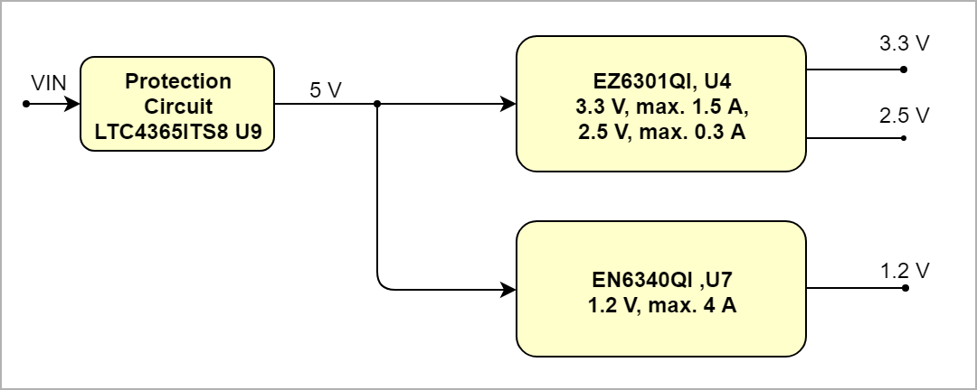
Power supply with minimum current capability of 1A 1 A for system startup is recommended.
...
Scroll Title
anchor
Figure_PWR_PD
title
Power Distribution
Scroll Ignore
draw.io Diagram
border
false
viewerToolbar
true
fitWindow
false
diagramDisplayName
lbox
true
revision
79
diagramName
TEI0009_PWR_PD
simpleViewer
false
width
links
auto
tbstyle
hidden
diagramWidth
639
Scroll Only
Power-On Sequence
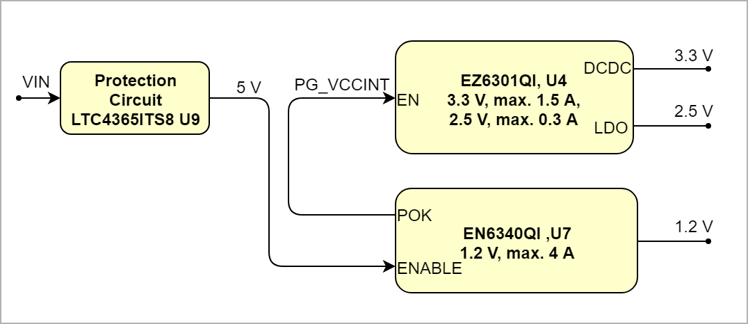
There is no the following power on sequence, After power on, all regulators will be enabled as you can see in . The DCDC converter U7 enables the device U4 according to the diagram below.
Scroll Title
anchor
Figure_PWR_PS
title
Power Sequency
Scroll Ignore
draw.io Diagram
border
false
viewerToolbar
true
fitWindow
false
diagramDisplayName
lbox
true
revision
67
diagramName
TEI0009_PWR_PS
simpleViewer
false
width
links
auto
tbstyle
hidden
diagramWidth
639518
Scroll Only
Voltage
...
Protection Circuit
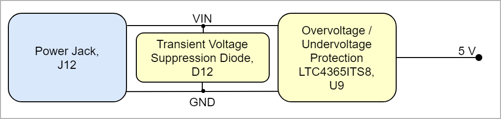
There is a diod transient voltage suppression diode (D12) which protects the board from reverse polarity, voltage spikes. Additionaly there is an Over/under voltage (IC) which protects the board from over voltage damagesovervoltage / undervoltage protection device (U9) for board protection.
Scroll Title
anchor
Figure_PWR_VMC
title
Voltage Monitor Circuit
Scroll Ignore
draw.io Diagram
border
false
viewerToolbar
true
fitWindow
false
diagramDisplayName
lbox
true
revision
13
diagramName
TEI0009_PWR_VM
simpleViewer
false
width
links
auto
tbstyle
hidden
diagramWidth
641490
Scroll Only
Power Rails
Scroll Title
anchor
Table_PWR_PR
title
Module power rails.
Scroll Table Layout
orientation
portrait
sortDirection
ASC
repeatTableHeaders
default
style
widths
sortByColumn
1
sortEnabled
false
cellHighlighting
true
Connector Designator
VCC / VCCIO Schematic Name
Pin
Direction
Notes
J12
5 V / VIN
1
In
J3
3.3 V / 3.3V
2, 4
Out
5 V / 5V
5
Out
J5
3.3 V / 3.3V
3
Out
Bank Voltages
Scroll Title
anchor
Table_PWR_BV
title
Zynq SoC bank voltages.
Scroll Table Layout
orientation
portrait
sortDirection
ASC
repeatTableHeaders
default
style
widths
sortByColumn
1
sortEnabled
false
cellHighlighting
true
Bank
Schematic Name
Voltage
Notes
Bank 1...8
VCCIO1...8
3.3V
Bank 2
VCCIO2
3.3V
Bank 3
VCCIO3
3.3V
Bank 4
VCCIO4
3.3V
Bank 5
VCCIO5
3.3V
Bank 6
VCCIO6
3.3V
Bank 7
VCCIO7
3.3V
Bank 8
VCCIO8
3.3V
Technical Specifications
Absolute Maximum Ratings
Technical Specifications
Absolute Maximum Ratings
Scroll Title
anchor
Table_TS_AMR
Scroll Title
anchor
Table_TS_AMR
title
Absolute maximum ratings
Scroll Table Layout
orientation
portrait
sortDirection
ASC
repeatTableHeaders
default
style
widths
sortByColumn
1
sortEnabled
false
cellHighlighting
true
Symbols
Description
Min
Max
Unit
Note
VIN
Input supply voltage (J12)
-4.5.0
5.05
V
VCCIO
AREF
External Reference Voltage for ADC/DAC (J1 - 8)
I/O buffers power supply
-0.
5
3
3.
75
6
V
VCCINT
Core voltage
-0.5
1.8
V
VCCD_PLL
PLL digital power supply
-0.5
1.8
V
VCCA
Phase-locked loop (PLL) analog power supply
-0.5
3.75
V
Only for input usage.
AIN0...5
Input Voltage for
V_AN
Analog Input Voltage on ADC/DAC (U2J4)
-0.3
3.6
V
V_DIG
Only for input usage.
AIN6...7
Input Voltage for Digital Input Voltage on ADC/DAC (U2TP1...2)
-0.3
3.6
V
Only for input usage.
EXT_RST
External Reset (J3 - 3
V_REF_IN
Internal Reference Voltage Voltage on ADC/DAC (U2)
-0.35
34.62
VV
D0_REF_EXRXD, D1_TXD, D2...7
Arduino Interface (J2External Reference Voltage Voltage on ADC/DAC (U2)