Page History
...
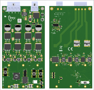
The Trenz Electronic CR00140-01 is an module a CRUVI motor driver module. It supports motors with up to 4 phases up to 40V.
Refer to http://trenz.org/tec0850-info for the current online version of this manual and other available documentation.
...
| Page properties | ||||
|---|---|---|---|---|
| ||||
Note: Key Features' must be split into 6 main groups for modues:
Key Features' must be split into 6 main groups for carrier:
|
- Modules/ SoC FPGA
- On Board
- MAX10 CPLD
- Interface
- CRUVI
- Power
- Dimension
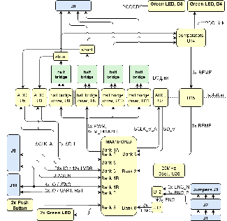
Block Diagram
- 2 phase current measurement
- DC_LINK voltage measurement
- 4x LEDs (2 power indicator, 2 user)
- 2x Pushbutton
- Interface
- 4 phase screw terminal motor connector
- CRUVI for control
- 1x high speed connector
- 1 low speed connector
- 6x1 pin header for single ended sensors
- 5x2 pin header for differential sensors
- Power
- screw terminal for up to 40 V DC motor supply
- Dimension
- 131 mm x 68.35 mm
Block Diagram
| Page properties | ||||
|---|---|---|---|---|
| ||||
| Page properties | ||||
| ||||
add drawIO object here.
|
...
| Scroll Title | ||||||||||||||||||||||||||
|---|---|---|---|---|---|---|---|---|---|---|---|---|---|---|---|---|---|---|---|---|---|---|---|---|---|---|
| ||||||||||||||||||||||||||
|
Main Components
| Page properties | ||||
|---|---|---|---|---|
| ||||
Notes :
|
| Scroll Title | ||||
|---|---|---|---|---|
| Scroll Title | ||||
| ||||
|
- ...
- ...
- ...
Initial Delivery State
| Page properties | ||||
|---|---|---|---|---|
| ||||
Notes : Only components like EEPROM, QSPI flash can be initialized by default at manufacture. If there is no components which might have initial data ( possible on carrier) you must keep the table empty |
...
| anchor | Table_OV_IDS |
|---|---|
| title | Initial delivery state of programmable devices on the module |
...
Storage device name
...
Content
...
Notes
...
Quad SPI Flash
...
Configuration Signals
| Page properties | ||||
|---|---|---|---|---|
| ||||
|
...
| anchor | Table_OV_BP |
|---|---|
| title | Boot process. |
...
MODE Signal State
...
| anchor | Table_OV_RST |
|---|---|
| title | Reset process. |
...
Signal
...
Signals, Interfaces and Pins
| Page properties | ||||
|---|---|---|---|---|
| ||||
Notes :
|
Board to Board (B2B) I/Os
FPGA bank number and number of I/O signals connected to the B2B connector:
...
| anchor | Table_SIP_B2B |
|---|---|
| title | General PL I/O to B2B connectors information |
...
JTAG access to the TExxxx SoM through B2B connector JMX.
...
| anchor | Table_SIP_JTG |
|---|---|
| title | JTAG pins connection |
...
JTAG Signal
...
B2B Connector
...
MIO Pins
...
| hidden | true |
|---|---|
| id | Comments |
you must fill the table below with group of MIOs which are connected to a specific components or peripherals, you do not have to specify pins in B2B, Just mention which B2B is connected to MIOs. The rest is clear in the Schematic.
Example:
|
- Motor connector screw terminal, J8
- Power supply screw terminal, J7
- 5x2 pinheader, base for TEI0004 JTAG programmer, J10
- 5x2 pinheader for sensor selection, J3
- 6x1 pinheader for single ended sensors, J1
- 5x2 pinheader for differential sensors, J2
- User push buttons, S1, S2
- User LEDs, D1, D2
- LED DC_Link, D4
- LED Power Good, D3
- DCDC for 15V, U1
- DCDC for 5V, U2
- half bridge drivers, U8, U9, U10, U11
- MAX10 CPLD, U25
- CRUVI high speed connector
- CRUVI low speed connector
- ADCs, U3, U5, U7
- Shunt resistors, R22, R28
Initial Delivery State
...
SPI_CS , SPI_DQ0... SPI_DQ3
SPI_SCK
...
| anchor | Table_OBP_MIOs |
|---|---|
| title | MIOs pins |
...
| Page properties | ||||
|---|---|---|---|---|
| ||||
Notes :
|
| Page properties | ||||
|---|---|---|---|---|
| ||||
Notes : In the on-board peripheral table "chip/Interface" must be linked to the corresponding chapter or subsection |
...
| anchor | Table_OBP |
|---|---|
| title | On board peripherals |
...
Quad SPI Flash Memory
| Page properties | ||||
|---|---|---|---|---|
| ||||
Notes :Minimum and Maximum density of quad SPI flash must be mentioned for other assembly options. Only components like EEPROM, QSPI flash can be initialized by default at manufacture. If there is no components which might have initial data ( possible on carrier) you must keep the table empty |
| Scroll Title | ||||||||||||||||||
|---|---|---|---|---|---|---|---|---|---|---|---|---|---|---|---|---|---|---|
| ||||||||||||||||||
| ||||||||||||||||||
| MIO Pin | Schematic | U?? Pin | Notes |
...
|
Signals, Interfaces and Pins
| Page properties | ||||
|---|---|---|---|---|
| ||||
Notes :
|
Board to Board (B2B) I/Os
FPGA bank number and number of I/O signals connected to the B2B connector:
| Scroll Title | ||||||||||||||||||||||||||
|---|---|---|---|---|---|---|---|---|---|---|---|---|---|---|---|---|---|---|---|---|---|---|---|---|---|---|
| ||||||||||||||||||||||||||
| Scroll Table Layout | ||||||||||||||||||||||||||
| orientation | portrait | |||||||||||||||||||||||||
| sortDirection | ASC | |||||||||||||||||||||||||
| repeatTableHeaders | default | style | widths | |||||||||||||||||||||||
| sortByColumn | 1 | |||||||||||||||||||||||||
| sortEnabled | false | |||||||||||||||||||||||||
| cellHighlighting | true | |||||||||||||||||||||||||
| MIO Pin | Schematic | U? Pin | Notes | |||||||||||||||||||||||
| Scroll Title | ||||||||||||||||||||||||||
| ||||||||||||||||||||||||||
MIO Pin | I2C Address | Designator
|
...
| anchor | Table_OBP_EEP |
|---|---|
| title | I2C EEPROM interface MIOs and pins |
|
JTAG Interface
JTAG access to the CPLD of CR00140 is possible via the CRUVI high speed connector J9 or the pinheader J10, which is a base for TEI004 JTAG programmer.
...
| Scroll Title | ||||||||||||||||||
|---|---|---|---|---|---|---|---|---|---|---|---|---|---|---|---|---|---|---|
| ||||||||||||||||||
| ||||||||||||||||||
| MIO Pin | I2C Address | Designator | Notes |
LEDs
...
| anchor | Table_OBP_LED |
|---|---|
| title | On-board LEDs |
|
On-board Peripherals
...
| Page properties | ||||
|---|---|---|---|---|
| ||||
Notes : Minimum and Maximum density of DDR3 SDRAM must be mentioned for other assembly options. (pay attention to supported address length for DDR3) |
The TE???? SoM has ??? GByte volatile DDR3 SDRAM IC for storing user application code and data.
- Part number:
- Supply voltage:
- Speed:
- NOR Flash
- Temperature:
...
|
LEDs
| Scroll Title | |||||||||||||||||||||||
|---|---|---|---|---|---|---|---|---|---|---|---|---|---|---|---|---|---|---|---|---|---|---|---|
| |||||||||||||||||||||||
Bank
Signal Name | ETH1 | ETH2 | Signal Description | |
CAN Transceiver
...
| anchor | Table_OBP_CAN |
|---|---|
| title | CAN Tranciever interface MIOs |
...
|
Buttons
...
| Scroll Title | |||||||||||||||||||||||||||||||||||||||
|---|---|---|---|---|---|---|---|---|---|---|---|---|---|---|---|---|---|---|---|---|---|---|---|---|---|---|---|---|---|---|---|---|---|---|---|---|---|---|---|
| |||||||||||||||||||||||||||||||||||||||
|
Power and Power-On Sequence
...
Overview
Content Tools