...
| Scroll Title |
|---|
| anchor | Figure_OV_BD |
|---|
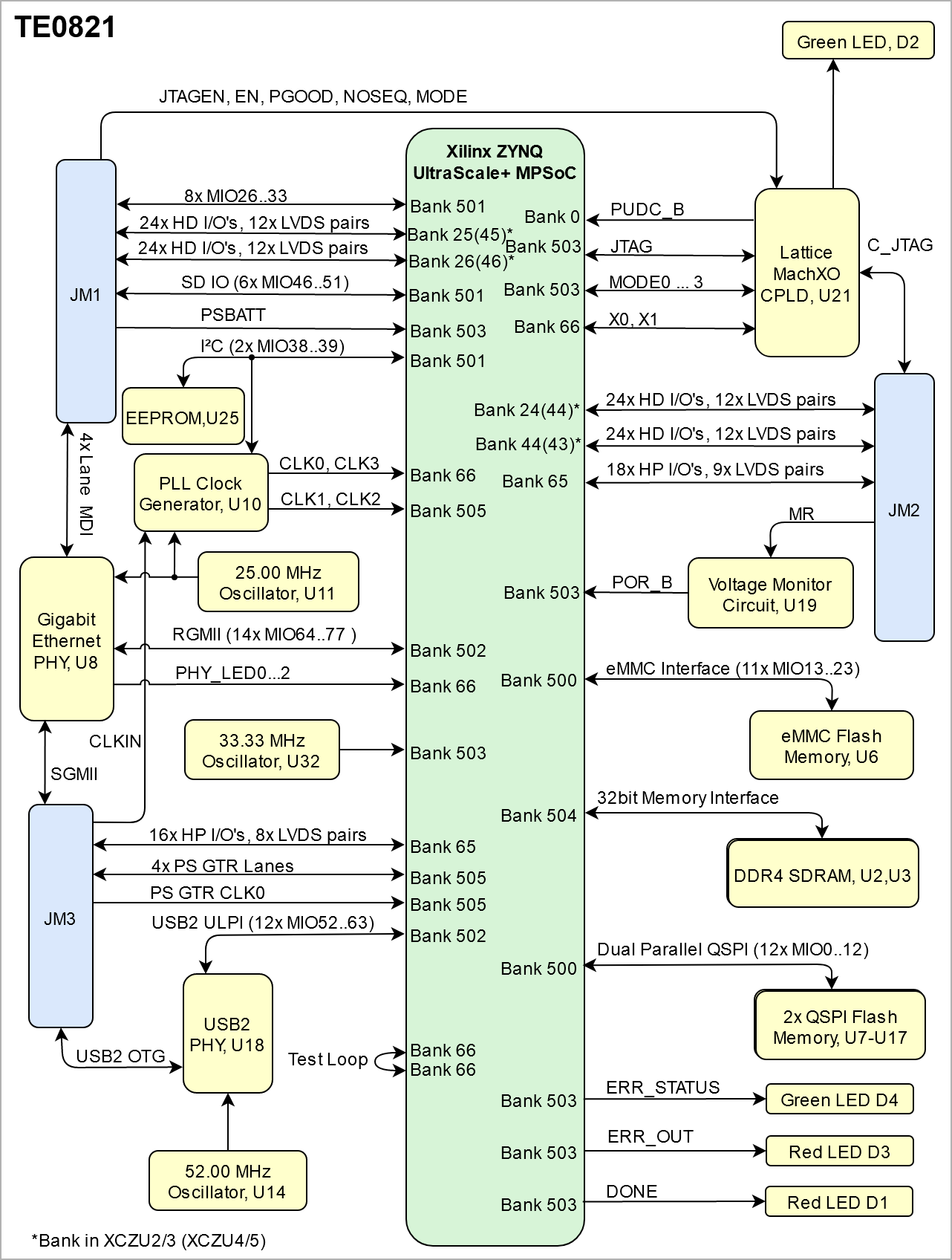
| title | TE0821 block diagram |
|---|
|
| Scroll Ignore |
|---|
| draw.io Diagram |
|---|
| border | false |
|---|
| |
|---|
| diagramName | TE0821_OV_BD |
|---|
| simpleViewer | false |
|---|
| width | |
|---|
| links | auto |
|---|
| tbstyle | hidden |
|---|
| diagramDisplayName | |
|---|
| lbox | true |
|---|
| diagramWidth | 641 |
|---|
| revision | 45 |
|---|
|
|
| Scroll Only |
|---|
|
|
Main Components
...
| Scroll Title |
|---|
| anchor | Table_OBP |
|---|
| title | On board peripherals |
|---|
|
| Scroll Table Layout |
|---|
| orientation | portrait |
|---|
| sortDirection | ASC |
|---|
| repeatTableHeaders | default |
|---|
| style | |
|---|
| widths | |
|---|
| sortByColumn | 1 |
|---|
| sortEnabled | false |
|---|
| cellHighlighting | true |
|---|
|
|
Quad SPI Flash Memory
| Page properties |
|---|
|
Notes : Minimum and Maximum density of quad SPI flash must be mentioned for other assembly options. |
...
| Scroll Title |
|---|
| anchor | Table_OBP_SPI |
|---|
| title | Quad SPI interface MIOs and pins |
|---|
|
| Scroll Table Layout |
|---|
| orientation | portrait |
|---|
| sortDirection | ASC |
|---|
| repeatTableHeaders | default |
|---|
| style | |
|---|
| widths | |
|---|
| sortByColumn | 1 |
|---|
| sortEnabled | false |
|---|
| cellHighlighting | true |
|---|
|
| Pin | Schematic | Notes |
|---|
| U7 Pin | U17 Pin |
|---|
| nCS | MIO5 | MIO7 |
| | CLK | MIO0 | MIO12 |
| | DI/IO0 | MIO4 | MIO8 |
| | DO/IO1 | MIO1 | MIO9 |
| | nHOLD/IO3 | MIO3 | MIO11 |
| | WP/IO2 | MIO2 | MIO10 |
|
|
EEPROM
There is a 2Kb EEPROM provided on the module TE0821.
| Scroll Title |
|---|
| anchor | Table_OBP_EEP |
|---|
| title | I2C EEPROM interface MIOs and pins |
|---|
|
| Scroll Table Layout |
|---|
| orientation | portrait |
|---|
| sortDirection | ASC |
|---|
| repeatTableHeaders | default |
|---|
| style | |
|---|
| widths | |
|---|
| sortByColumn | 1 |
|---|
| sortEnabled | false |
|---|
| cellHighlighting | true |
|---|
|
| MIO Pin | Schematic | U25 Pin | Notes |
|---|
| MIO39 | I2C_SDA | SDA |
| | MIO38 | I2C_SCL | SCL |
|
|
...
| Scroll Title |
|---|
| anchor | Table_OBP_LED |
|---|
| title | On-board LEDs |
|---|
|
| Scroll Table Layout |
|---|
| orientation | portrait |
|---|
| sortDirection | ASC |
|---|
| repeatTableHeaders | default |
|---|
| style | |
|---|
| widths | |
|---|
| sortByColumn | 1 |
|---|
| sortEnabled | false |
|---|
| cellHighlighting | true |
|---|
|
| Designator | Color | Connected to | Active Level | Note |
|---|
| D1 | Red | DONE | HighLow |
| | D2 | Green | ERRUSR_STATUSLED | High |
| | D3 | Red | ERR_OUT | High |
| | D4 | Green | ERR_STATUS | High |
|
|
DDR4 SDRAM
| Page properties |
|---|
|
Notes : Minimum and Maximum density of DDR3 SDRAM must be mentioned for other assembly options. (pay attention to supported address length for DDR3) |
...
| Scroll Title |
|---|
| anchor | Table_OBP_ETH |
|---|
| title | Ethernet PHY to Zynq SoC connections |
|---|
|
| Scroll Table Layout |
|---|
| orientation | portrait |
|---|
| sortDirection | ASC |
|---|
| repeatTableHeaders | default |
|---|
| style | |
|---|
| widths | |
|---|
| sortByColumn | 1 |
|---|
| sortEnabled | false |
|---|
| cellHighlighting | true |
|---|
|
| Pin | Schematic | Connected to | Note |
|---|
| MDIP0...3 | PHY_MDI0...3 | B2B, JM1 |
| | MDC | ETH_MDC | MIO76 |
| | MDIO | ETH_MDIO | MIO77 |
| | S_IN | S_IN | B2B, JM3 |
| | S_OUT | S_OUT | B2B, JM3 |
| | TXD0..3 | ETH_TXD0...3 | MIO65...68 |
| | TX_CTRL | ETH_TXCTL | MIO69 |
| | TX_CLK | ETH_TXCK | MIO64 |
| | RXD0...3 | ETH_RXD0...3 | MIO71...74 |
| | RX_CTRL | ETH_RXCTL | MIO75 |
| | RX_CLK | ETH_RXCK | MIO70 |
| | LED0...2 | PHY_LED0...2 | FPGA Bank 66 |
| | RESETn | ETH_RST | MIO24 |
|
|
Clock Sources
| Scroll Title |
|---|
| anchor | Table_OBP_CLK |
|---|
| title | Osillators |
|---|
|
| Scroll Table Layout |
|---|
| orientation | portrait |
|---|
| sortDirection | ASC |
|---|
| repeatTableHeaders | default |
|---|
| style | |
|---|
| widths | |
|---|
| sortByColumn | 1 |
|---|
| sortEnabled | false |
|---|
| cellHighlighting | true |
|---|
|
| Designator | Description | Frequency | Note |
|---|
| U11 | MEMS Oscillator | 25 MHz |
| | U14 | MEMS Oscillator | 52 MHz |
| | U32 | MEMS Oscillator | 80 MHz |
|
|
...
There is a programmable clock generator on-board (U??U10) provided in order to generate variable clocks for the module. Programming can be done using I2C via PIN header J??. The I2C Address is 0x??0x70 or 0x71.
| Scroll Title |
|---|
| anchor | Table_OBP_PCLK |
|---|
| title | Programmable Clock Generator Inputs and Outputs |
|---|
|
| Scroll Table Layout |
|---|
| orientation | portrait |
|---|
| sortDirection | ASC |
|---|
| repeatTableHeaders | default |
|---|
| sortByColumn | 1 |
|---|
| sortEnabled | false |
|---|
| cellHighlighting | true |
|---|
|
U?? U25 Pin
| Signal | Connected to | Direction | Note |
|---|
IN0 | IN1 | IN2 | IN3 | XAXB | SCLK | SDA | ..1 | CLK_IN | JM3 | IN |
| | IN2 | CLK_25M | Oscillator, U11 | IN |
| | SCL | I2C_SCL | EEPROM,U25 | INOUT |
| | SDA | I2C_SDA | EEPROM,U25 | INOUT |
| | CLK0 | CLK0 | JM3 | OUT |
| | CLK1 | B505_CLK3 | FPGA Bank 505 | IN |
| | CLK2 | B505_CLK1 | FPGA Bank 505 | IN |
| | CLK3 | CLK3_N |
| IN | OUT0 | OUT1 | OUT2 | OUT3 | OUT4 | OUT5 | OUT6 | OUT7 | OUT8/OUT9 |
|
|
Power and Power-On Sequence
...
| Scroll Title |
|---|
| anchor | Table_PWR_BV |
|---|
| title | Zynq SoC bank voltages. |
|---|
|
| Scroll Table Layout |
|---|
| orientation | portrait |
|---|
| sortDirection | ASC |
|---|
| repeatTableHeaders | default |
|---|
| style | |
|---|
| widths | |
|---|
| sortByColumn | 1 |
|---|
| sortEnabled | false |
|---|
| cellHighlighting | true |
|---|
|
| Schematic Name | | Notes |
|---|
| 64 HP | VCCO_64 | User | HP: 1.0V to 1.8V | | 65 HP | VCCO_65 | User | HP: 1.0V to 1.8V | | 66 HP | VCCO_66 | User | HP: 1.0V to 1.8V | | 500 PSMIO | VCCO_PSIO0_500 | 1.8V | - | | 501 PSMIO | VCCO_PSIO1_501 | 3.3V | - | | 502 PSMIO | VCCO_PSIO2_502 | 1.8V | - | | 503 PSCONFIG | VCCO_PSIO3_503 | 1.8V | - | | 504 PSDDR | VCCO_PSDDR_504 | 1.2V | - |
|
Board to Board Connectors
...