...
| Scroll Title |
|---|
| anchor | Table_SIP_ETH |
|---|
| title | GigaBit Ethernet connection |
|---|
|
| Scroll Table Layout |
|---|
| orientation | portrait |
|---|
| sortDirection | ASC |
|---|
| repeatTableHeaders | default |
|---|
| style | |
|---|
| widths | |
|---|
| sortByColumn | 1 |
|---|
| sortEnabled | false |
|---|
| cellHighlighting | true |
|---|
|
| Pin | Schematic | Connected to | Note |
|---|
| MDIP0...3 | PHY_MDI0...3 | B2B, JM1 |
| | MDC | ETH_MDC | MIO76 |
| | MDIO | ETH_MDIO | MIO77 |
| | S_IN | S_IN | B2B, JM3 |
| | S_OUT | S_OUT | B2B, JM3 |
| | TXD0..3 | ETH_TXD0...3 | MIO65...68 |
| | TX_CTRL | ETH_TXCTL | MIO69 |
| | TX_CLK | ETH_TXCK | MIO64 |
| | RXD0...3 | ETH_RXD0...3 | MIO71...74 |
| | RX_CTRL | ETH_RXCTL | MIO75 |
| | RX_CLK | ETH_RXCK | MIO70 |
| | LED0...2 | PHY_LED0...2 | FPGA Bank 66 |
| | RESETn | ETH_RST | MIO24 |
|
|
System Controller CPLD
Special purpose pins are connected to System Controller CPLD and have following default configuration:
| Scroll Title |
|---|
| anchor | Table_SIP_CPLD |
|---|
| title | System Controller CPLD special purpose pins |
|---|
|
| Scroll Table Layout |
|---|
| orientation | portrait |
|---|
| sortDirection | ASC |
|---|
| repeatTableHeaders | default |
|---|
| style | |
|---|
| widths | |
|---|
| sortByColumn | 1 |
|---|
| sortEnabled | false |
|---|
| cellHighlighting | true |
|---|
|
| Pin Name | Mode | Function | Default Configuration |
|---|
| EN1 | Input | Power Enable | No hard wired function on PCB. When forced low, PGOOD goes low without effect on power management | | PGOOD | Output | Power Good | Only indirect used for power status, see CPLD description | | NOSEQ | - | - | No used for Power sequencing, see CPLD description | | RESIN | Input | Reset | Active low reset, gated to POR_B | | JTAGEN | Input | JTAG Select | Low for normal operation, high for CPLD JTAG access |
|
USB Interface
USB PHY is provided by Microchip USB3320. The ULPI interface is connected to the Zynq PS USB0. I/O voltage is fixed at 1.8V. Reference clock input for the USB PHY is supplied by the on-board 52.00 MHz oscillator (U14).
| Scroll Title |
|---|
| anchor | Table_SIP_USB |
|---|
| title | General overview of the USB PHY signals |
|---|
|
| Scroll Table Layout |
|---|
| orientation | portrait |
|---|
| sortDirection | ASC |
|---|
| repeatTableHeaders | default |
|---|
| style | |
|---|
| widths | |
|---|
| sortByColumn | 1 |
|---|
| sortEnabled | false |
|---|
| cellHighlighting | true |
|---|
|
| PHY Pin | ZYNQ Pin | B2B Name | Notes |
|---|
| ULPI | MIO52..63 | - | Zynq USB0 MIO pins are connected to the USB PHY. | | REFCLK | - | - | 52.000000 MHz from on-board oscillator (U14). | | REFSEL[0..2] | - | - | Reference clock frequency select, all set to GND selects 52.000000 MHz. | | RESETB | MIO25 | - | Active low reset. | | CLKOUT | MIO52 | - | Connected to 1.8V, selects reference clock operation mode. | | DP, DM | - | OTG_D_P, OTG_D_N | USB data lines routed to B2B connector JM3 pins 47 and 49. | | CPEN | - | VBUS_V_EN | External USB power switch active high enable signal, routed to JM3 pin 17. | | VBUS | - | USB_VBUS | Connect to USB VBUS via a series of resistors, see reference schematics, routed to JM3 pin 55. | | ID | - | OTG_ID | For an A-device connect to ground, for a B-device left floating. routed from JM3 pin 23. |
|
MIO Pins
| Page properties |
|---|
|
you must fill the table below with group of MIOs which are connected to a specific components or peripherals, you do not have to specify pins in B2B, Just mention which B2B is connected to MIOs. The rest is clear in the Schematic. Example: | MIO Pin | Connected to | B2B | Notes |
|---|
| MIO12...14 | SPI_CS , SPI_DQ0... SPI_DQ3, SPI_SCK | J2 | QSPI |
|
...
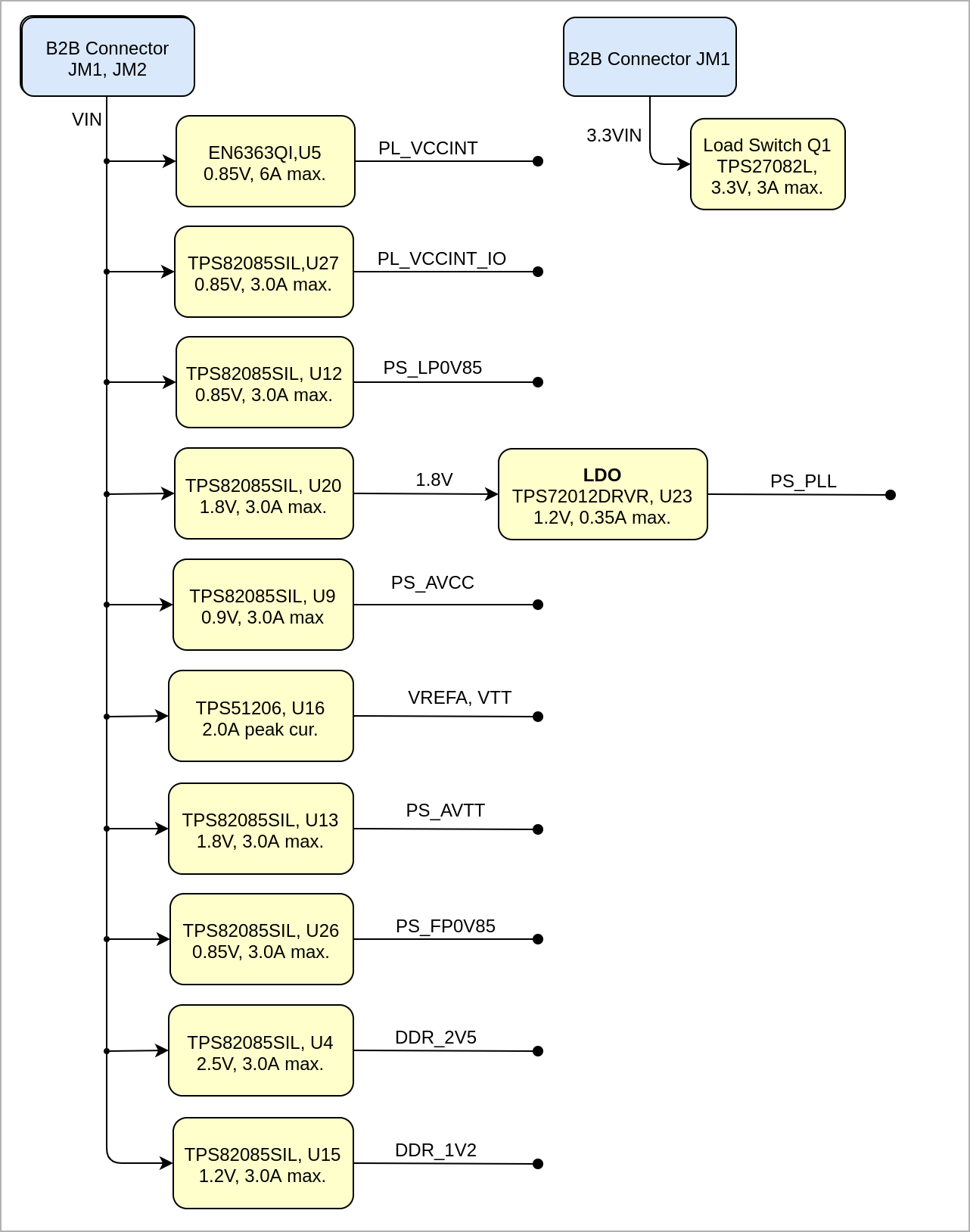
| Scroll Title |
|---|
| anchor | Figure_PWR_PD |
|---|
| title | Power Distribution |
|---|
|
| Scroll Ignore |
|---|
| draw.io Diagram |
|---|
| border | false |
|---|
| |
|---|
| diagramName | TE0821_PWR_PD |
|---|
| simpleViewer | false |
|---|
| width | |
|---|
| links | auto |
|---|
| tbstyle | hidden |
|---|
| diagramDisplayName | |
|---|
| lbox | true |
|---|
| diagramWidth | 641 |
|---|
| revision | 45 |
|---|
|
|
| Scroll Only |
|---|
|
|
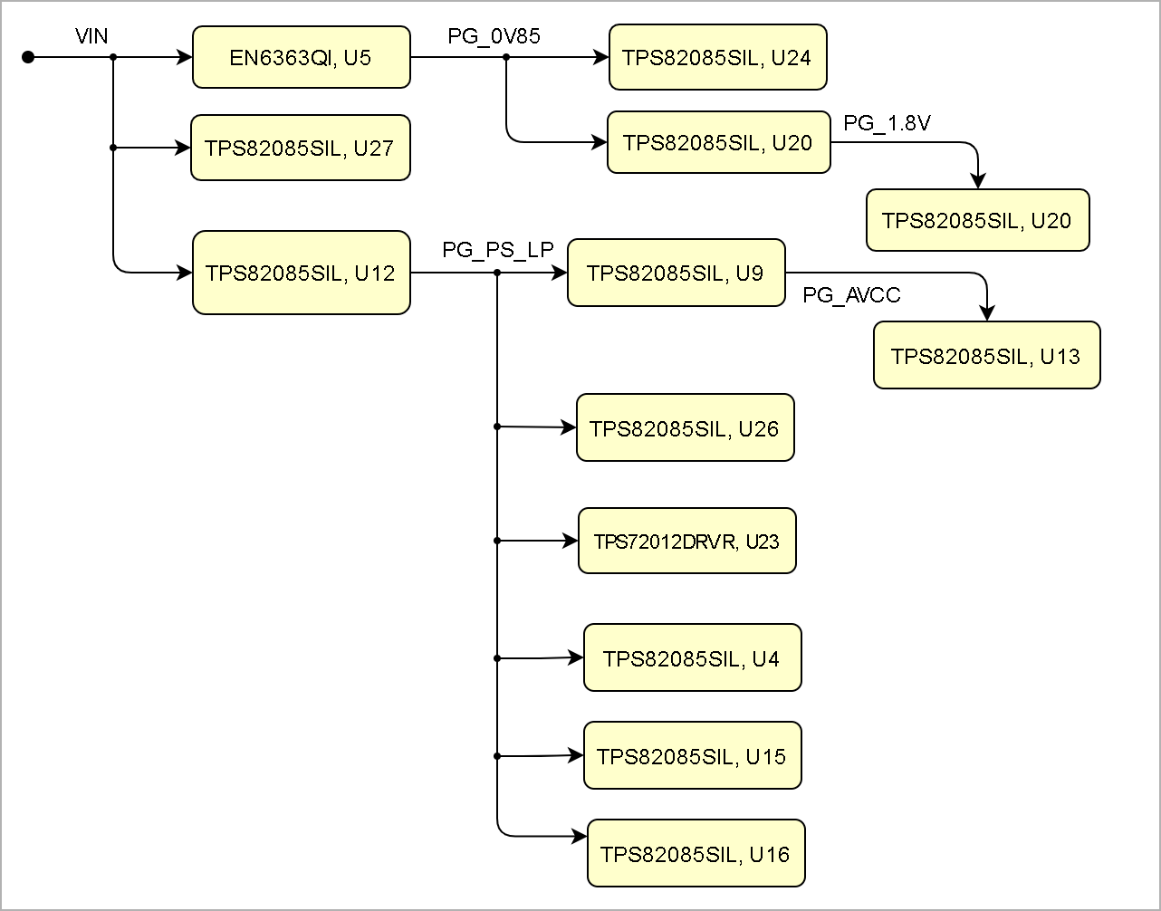
Power-On Sequence
| Scroll Title |
|---|
| anchor | Figure_PWR_PS |
|---|
| title | Power Sequency |
|---|
|
| Scroll Ignore |
|---|
| draw.io Diagram |
|---|
| border | false |
|---|
| |
|---|
| diagramName | TE0821_PWR_PS |
|---|
| simpleViewer | false |
|---|
| width | |
|---|
| links | auto |
|---|
| tbstyle | hidden |
|---|
| diagramDisplayName | |
|---|
| lbox | true |
|---|
| diagramWidth | 641 |
|---|
| revision | 46 |
|---|
|
|
| Scroll Only |
|---|
|
|
Power Rails
| Scroll Title |
|---|
| anchor | Table_PWR_PR |
|---|
| title | Module power rails. |
|---|
|
| Scroll Table Layout |
|---|
| orientation | portrait |
|---|
| sortDirection | ASC |
|---|
| repeatTableHeaders | default |
|---|
| style | |
|---|
| widths | |
|---|
| sortByColumn | 1 |
|---|
| sortEnabled | false |
|---|
| cellHighlighting | true |
|---|
|
| Power Rail Name | B2B JM1 Pin | B2B JM2 Pin | Direction | Notes |
|---|
| VIN | 1, 3, 5 | 2, 4, 6, 8 | Input | Supply voltage from the carrier board | | 3.3V | - | 10, 12 | Output | Internal 3.3V voltage level | | 3.3VIN | 13, 15 | - | Input | Supply voltage from the carrier board | | 1.8V | 39 | - | Output | Internal 1.8V voltage level | | JTAG VREF | - | 91 | Output | JTAG reference voltage.
Attention: Net name on schematic is "3.3VIN" | | VCCO_64 | - | 7, 9 | Input | High performance I/O bank voltage | | VCCO_65 | - | 5 | Input | High performance I/O bank voltage | | VCCO_66 | 9, 11 | - | Input | High performance I/O bank voltage |
|
...
| Scroll Title |
|---|
| anchor | Table_TS_AMR |
|---|
| title | PS absolute maximum ratings |
|---|
|
| Scroll Table Layout |
|---|
| orientation | portrait |
|---|
| sortDirection | ASC |
|---|
| repeatTableHeaders | default | style | widths |
|---|
| sortByColumn | 1 |
|---|
| sortEnabled | false |
|---|
| cellHighlighting | true |
|---|
| | style | |
|---|
| widths | |
|---|
| sortByColumn | 1 |
|---|
| sortEnabled | false |
|---|
| cellHighlighting | true |
|---|
|
| Description | Min | Max | Unit | Notes |
|---|
VIN supply voltage | -0.3 | 7 | V | See EN6347QI and TPS82085SIL datasheets | | 3.3VIN supply voltage | -0.1 | 3.630 | V | Xilinx DS925 and TPS27082L datasheet | | PS I/O supply voltage, VCCO_PSIO | -0.5 | 3.630 | V | Xilinx document DS925 | | PS I/O input voltage | -0.5 | VCCO_PSIO + 0.55 | V | Xilinx document DS925 | | HP I/O bank supply voltage, VCCO | -0.5 | 2.0 | V | Xilinx document DS925 | | HP I/O bank input | | Description | Min | Max | Unit | Notes |
|---|
| VIN supply voltage | -0.355 | VCCO + 0.557 | V | See EN6347QI and TPS82085SIL datasheets | Xilinx document DS925 | | PS GTR reference clocks absolute input 3.3VIN supply voltage | -0.5 | 13.6301 | V | Xilinx DS925 and TPS27082L datasheetdocument DS925 | | PS | I/O supply voltage, VCCO_PSIOGTR absolute input voltage | -0.5 | 31. | 6301 | V | Xilinx document DS925 | PS I/O input voltage Voltage on SC CPLD pins | -0.5 | VCCO_PSIO + 0.55 | V | Xilinx document DS925 | | HP I/O bank supply voltage, VCCO | -0.5 | 2.0 | V | Xilinx document DS925 | | HP I/O bank input voltage | -0.55 | VCCO + 0.55 | V | Xilinx document DS925 | | PS GTR reference clocks absolute input voltage | -0.5 | 1.1 | V | Xilinx document DS925 | | PS GTR absolute input voltage | -0.5 | 1.1 | V | Xilinx document DS925 | Voltage on SC CPLD pins | -0.5 | 3.75 | V | Lattice Semiconductor MachXO2 datasheet | Storage temperature | -40 | +85 | °C | See eMMC datasheet |
|
Recommended Operating Conditions
Operating temperature range depends also on customer design and cooling solution. Please contact us for options.
| 3.75 | V | Lattice Semiconductor MachXO2 datasheet | Storage temperature | -40 | +85 | °C | See eMMC datasheet |
|
Recommended Operating Conditions
Operating temperature range depends also on customer design and cooling solution. Please contact us for options.
| Scroll Title |
|---|
| anchor | Table_TS_ROC |
|---|
| title | Recommended operating conditions. |
|---|
|
| Scroll Table Layout |
|---|
| orientation | portrait |
|---|
| sortDirection | ASC |
|---|
| repeatTableHeaders | default |
|---|
| style | |
|---|
| widths | |
|---|
| sortByColumn | 1 |
|---|
| sortEnabled | false |
|---|
| cellHighlighting | true |
|---|
|
| Parameter | Min | Max | Units | Reference Document |
|---|
| VIN supply voltage | 3.3 | 6 | V | See TPS82085S datasheet | | 3.3VIN supply voltage | 3.3 | 3.465 | V | See LCMXO2-256HC, Xilinx DS925 datasheet | | PS I/O supply voltage, VCCO_PSIO | 1.710 | 3.465 | V | Xilinx document DS925 | | PS I/O input voltage | –0.20 | VCCO_PSIO + 0.20 | V | Xilinx document DS925 | | HP I/O banks supply voltage, VCCO | 0.950 | 1.9 | V | Xilinx document DS925 | | HP I/O banks input voltage | -0.20 | VCCO + 0.20 | V | Xilinx document DS925 | | Voltage on SC CPLD pins | -0.3 | 3.6 | V | Lattice Semiconductor MachXO2 datasheet | | Operating Temperature Range | 0 | 85 | °C | Xilinx document DS925, extended grade Zynq temperarure range |
|
| Scroll Title |
|---|
| anchor | Table_TS_ROC |
|---|
| title | Recommended operating conditions. |
|---|
|
| Scroll Table Layout |
|---|
|
| orientation | portrait |
|---|
| sortDirection | ASC |
|---|
| repeatTableHeaders | default |
|---|
style | widths | | sortByColumn | 1 |
|---|
| sortEnabled | false |
|---|
| cellHighlighting | true |
|---|
| Parameter | Min | Max | Units | Reference Document |
|---|
| V | See ???? datasheets. | V | See Xilinx ???? datasheet. | °C | See Xilinx ???? datasheet. | °C | See Xilinx ???? datasheet. |
Physical Dimensions
Module size: 40 mm × 50 mm. Please download the assembly diagram for exact numbers.
Mating height with standard connectors: 8 mm.
...