...
Overview
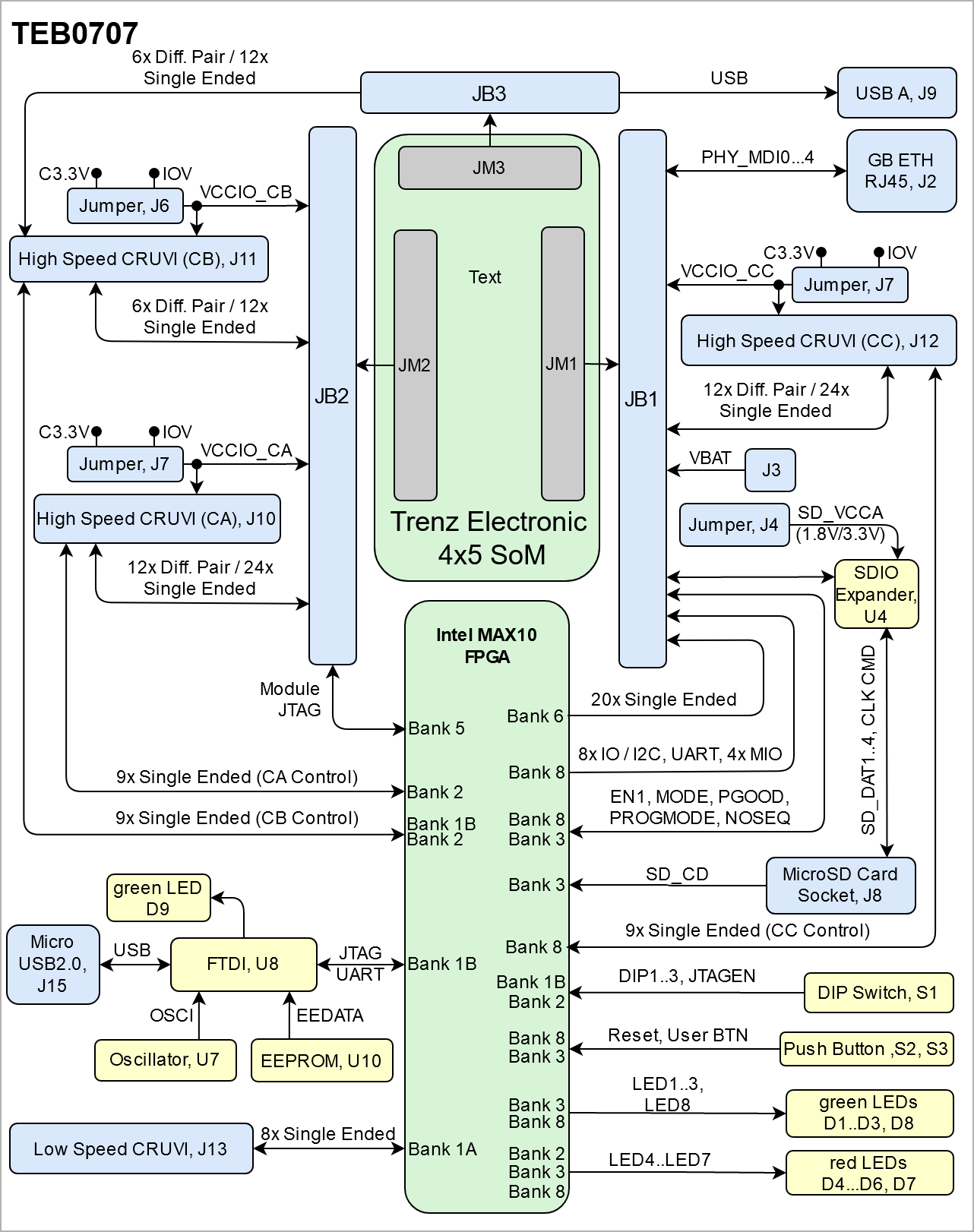
The Trenz Electronic TEM0707 is an industrial-grade module TEB0707 is a carrier for 4 x 5 Trenz Electronic modules. It provides three high speed and one low speed CRUVI extension connectors. For more information, please refer to the CRUVI B2B Connectors. The TEB0707 is integrated with an Intel MAX10 FPGA as system controller and it is equipped with a Micro USB2.0 Socket with FTDI to JTAG/UART solution, RJ45 LAN Socket, Micro USB A Socket, Micro SD Card Socket, Low and High Speed Board to Board Connectors, User LEDs, FTDI, Push Buttons and DIP Switch Switches for controlling the SoM. Furtheremore, the TEB0707 provides CRUVI Extension connectors. For more information, Please refer to the CRUVI B2B Connectors.
Refer to http://trenz.org/teb0707-info for the current online version of this manual and other available documentation.
...
- Modules
- 4x5 Trenz Electronic modules
- RAM/Storage
- EEPROM (FTDI Configuration)
- On Board
- Intel Max 10 FPGA
- FTDI FT2223
- 8x Green 6x User LEDs (3x green, 3x red)
- 2x Status LED
- DIP Switch
- Push Buttons
- Interface
- Gigabit RJ45 LAN socket
- SD Card socket
- Micro USB2.0 Socket
- USB A Socket
- 3x High Speed CRUVI B2B Connectors
- 1x Low Speed CRUVI B2B Connector
- 4x Jumpers
- Power
- Dimension
- Notes
...
| Scroll Title |
|---|
| anchor | Figure_OV_BD |
|---|
| title | TEB0707 block diagram |
|---|
|
| Scroll Ignore |
|---|
| draw.io Diagram |
|---|
| border | false |
|---|
| |
|---|
| diagramName | TEB0707_OV_BD |
|---|
| simpleViewer | false |
|---|
| width | 639 |
|---|
| links | auto |
|---|
| tbstyle | hidden |
|---|
| diagramDisplayName | |
|---|
| lbox | true |
|---|
| diagramWidth | 641 |
|---|
| revision | 2123 |
|---|
|
|
| Scroll Only |
|---|
| |
|
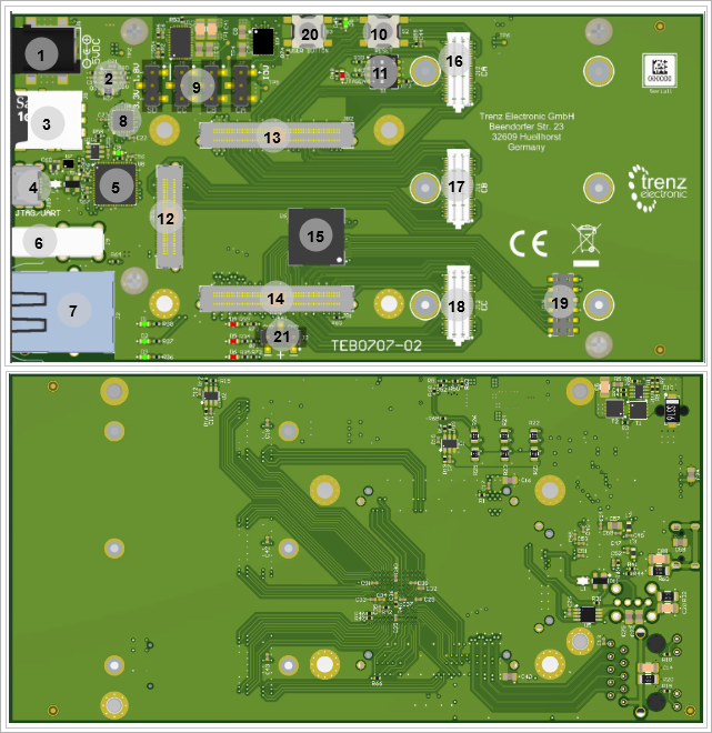
Main Components
| Page properties |
|---|
|
Notes : - Picture of the PCB (top and bottom side) with labels of important components
- Add List below
| Note |
|---|
For more information regarding how to add board photoes, Please refer to "Diagram Drawing Guidline" . | draw.io Diagram |
|---|
| border | false |
|---|
| |
|---|
| diagramName | TEB0707_OV_BD |
|---|
| simpleViewer | false |
|---|
| width | 639 |
|---|
| links | auto |
|---|
| tbstyle | hidden |
|---|
| diagramDisplayName | |
|---|
| lbox | true |
|---|
| diagramWidth | 641 |
|---|
| revision | 2123 |
|---|
|
|
|
| Scroll Title |
|---|
| anchor | Figure_OV_MC |
|---|
| title | TEB0707 main components |
|---|
|
| Scroll Ignore |
|---|
| draw.io Diagram |
|---|
| border | false |
|---|
| |
|---|
| diagramName | TEB0707_OV_MC |
|---|
| simpleViewer | false |
|---|
| width | 639 |
|---|
| links | auto |
|---|
| tbstyle | hidden |
|---|
| diagramDisplayName | |
|---|
| lbox | true |
|---|
| diagramWidth | 641 |
|---|
| revision | 46 |
|---|
|
|
| Scroll Only |
|---|
|
|
- Barrel Jack Power Supply, J1
- Voltage Regulator, U1
- Micro SD Card Socket, J8
- Micro USB2.0 Socket, J15
- FT2232H FTDI, U8
- USB A Socket, J9
- RJ45 LAN Socket, J2
- SDIO Port Expander, U4
- Jumpers, J4...7
- Push Button (Reset), S2
- DIP Switch, S1
- B2B Connector, JB3
- B2B Connector, JB2
- B2B Connector, JB1
- Intel MAX 10 FPGA, U6
- High speed Speed CRUVI Connector, J10
- High speed Speed CRUVI Connector, J11
- High speed Speed CRUVI Connector, J12
- Low Speed CRUVI Connector, J13
- User Push Button, S3
- JumperPin header, J3
Initial Delivery State
...
Interfaces and Number of I/O signals connected to the B2B connectors for Trenz 4x5 modules:
| Scroll Title |
|---|
| anchor | Table_SIP_B2B |
|---|
| title | General PL I/O to B2B connectors information |
|---|
|
| Scroll Table Layout |
|---|
| orientation | portrait |
|---|
| sortDirection | ASC |
|---|
| repeatTableHeaders | default |
|---|
| style | |
|---|
| widths | |
|---|
| sortByColumn | 1 |
|---|
| sortEnabled | false |
|---|
| cellHighlighting | true |
|---|
|
| B2B Connector | Interface | I/O Signal Count | Connected to | Notes |
|---|
JB1
| Ethernet LAN | 8x Single ended, 4x Diff pairs | RJ45 Socket, J2 |
| | SD Card | 6 x Single Ended | IO Expander, U4 |
| | I/Os | 20x Single Ended | MAX10 FPGA BAnk Bank 6, U6 |
| | CRUVI | 20x 12x Diff pairs/24x Single ended, 10x Diff pairs 4x Single Ended | High Speed CRUVI, J12 | CRUVI C | | SoM Control Signals | 5x Single Ended | MAX10 FPGA, U6 |
| | I/Os | 8x Single ended | MAX10 FPGA Bank 8, U6 | VBAT | 1x Single Ended | Pin Header, J3 |
| JB2
| CRUVI | 8x 12x Diff pairs/24x Single ended, 4x Diff pairs 4x Single Ended | High Speed CRUVI, J10 | CRUVI A | | CRUVI | 6x Diff pairs/12x Single ended, 6x Diff pairs | High Speed CRUVI, J11 | CRUVI B | | JTAG | 4x Single Ended | FPGA Bank 5, U6 |
| | JB3 | CRUVI | 6x Diff pairs/12x Single ended, 6x Diff pairs 4x Single Ended | High Speed CRUVI, J11 | CRUVI B | | USB | 1x Diff pair, 2x 4x Single Ended | USB A, J9 |
|
|
CRUVI B2B Connectors
...
| Scroll Title |
|---|
| anchor | Table_SIP_CRUVIB2B |
|---|
| title | CRUVI B2B connectors information |
|---|
|
| Scroll Table Layout |
|---|
| orientation | portrait |
|---|
| sortDirection | ASC |
|---|
| repeatTableHeaders | default |
|---|
| style | |
|---|
| widths | |
|---|
| sortByColumn | 1 |
|---|
| sortEnabled | false |
|---|
| cellHighlighting | true |
|---|
|
| Speed | Designators | Schematic | Connected to | Notes |
|---|
| High
| CRUVI C, J12 | A0...A5 (N/P) | B2B, JB1 |
| | B0...B5 (N/P) | B2B, JB1 |
| | MODE, REFCLK | FPGA Bank 8, | U6 SMB_ALERT, SMB_SDA, SMB_SCL | FPGA Bank 8, U6 | DI, SEL, DO, DI, SCK,SEL | MAX10 FPGA Bank 8, U6 | 3.3V User IOs (Max10 Firmware dependent) | | HSIO, HI, HO | B2B, | JB1 RESET | B2B, JB1 |
| | High
| CRUVI B, J11 | A0...A5 (N/P) | B2B, JB1 |
| | B0...B5 (N/P) | B2B, JB1 |
| | MODE, REFCLK | FPGA Bank 3, | U6 SMB_ALERT, SMB_SDA, SMB_SCL | FPGA Bank 2, U6 | DI, SEL, DO, DI, SCK,SEL | MAX10 FPGA Bank 2/3, U6 | 3.3V User IOs (Max10 Firmware dependent) | | HSIO, HIHSI, HO | B2BHSO, | JB3 RESET | B2B, JB3 |
| | High
| CRUVI A, J13
| A0...A5 (N/P) | B2B, JB2 |
| | B0...B5 (N/P) | B2B, JB2 |
| MODE, REFCLK | FPGA Bank 2, | U6 SMB_ALERT, SMB_SDA, SMB_SCL | FPGA Bank 3, U6 | DI , SEL, DO, DI, SCK ,SEL | MAX10 FPGA Bank 2/3, U6 | 3.3V User IOs (Max10 Firmware dependent) | | HSIO, HIHSI, HO | B2BHSO, | JB2 RESET | B2B, JB2 |
| | Low | CRUVI | X0...X7 | MAX10 FPGA Bank 1A, U6 |
|
|
JTAG Interface
JTAG
...
signals form FTDI U8 are routed to MAX10 CPLD. Via dip setting JTAG of MAX10 or JTAG of the connected Trenz 4x5 module can be selected. Forwarding signals to SoM is MAX10 Firmware dependent.
...
| scroll-title |
|---|
| anchor | Table_SIP_MJTG |
|---|
| title | JTAG pins connection |
|---|
|
| Scroll Table Layout |
|---|
| orientation | portrait |
|---|
| sortDirection | ASC |
|---|
| repeatTableHeaders | default |
|---|
| style | |
|---|
| widths | |
|---|
| sortByColumn | 1 |
|---|
| sortEnabled | false |
|---|
| cellHighlighting | true |
|---|
|
B2B Connector | | M_TMS | JB2-94 | | M_TDI | JB2-96 | | M_TDO | JB2-100 | | M_TCK | JB2-98 | | VCCJTAG | JB2-92 | |
...
| MAX10 Pin Bank 1B, U6 | Connected to |
|---|
| TMS | G1 | FTDI (U8) - ADBUS3 | | TDI | F5 | FTDI (U8) - ADBUS1 | | TDO | F6 | FTDI (U8) - ADBUS2 | | TCK | G2 | FTDI (U8) - ADBUS0 | | JTAGEN | E5 | Dip S1-4 |
|
JTAG access to the Trenz 4x5 module is through B2B connector JB2.
| Scroll Title |
|---|
| anchor | Table_SIP_MJTG |
|---|
| title | JTAG pins connection |
|---|
|
| Scroll Table Layout |
|---|
| orientation | portrait |
|---|
| sortDirection | ASC |
|---|
| repeatTableHeaders | default |
|---|
| style | |
|---|
| widths | |
|---|
| sortByColumn | 1 |
|---|
| sortEnabled | false |
|---|
| cellHighlighting | true |
|---|
|
Connected to | MAX10 Pin Bank5, U6 | B2B Connector |
|---|
| M_TMS |
FTDI (U8) - ADBUS3FTDI (U8) - ADBUS1FTDI (U8) - ADBUS2 | | M_TCK | FTDI (U8) - ADBUS0 | |
...
| J10 | JB2-100 | | M_TCK | H8 | JB2-98 | | VCCJTAG | J11, J12 | JB2-92 |
|
SD Card socket
The TEB0707 is equipped with an Micro SD Card readerslot, J8. Data for USBs are expanded through For levelshifting an IO Expander (U4) is used.
| Scroll Title |
|---|
| anchor | Table_SIP_SD Card |
|---|
| title | USB2.0 Socket information |
|---|
|
| Scroll Table Layout |
|---|
| orientation | portrait |
|---|
| sortDirection | ASC |
|---|
| repeatTableHeaders | default |
|---|
| style | |
|---|
| widths | |
|---|
| sortByColumn | 1 |
|---|
| sortEnabled | false |
|---|
| cellHighlighting | true |
|---|
|
| Pin | Schematic | Connected to | Notes |
|---|
| DAT0...3 | ESD_DAT0...3 | B2B, JB1 | Through IO Expander, U4 | | CMD | ESD_CMD | B2B, JB1 | Through IO Expander, U4 | | VDD | 3.3V_SD | B2B, JB1 | Through IO Expander, U4 | | CLK | ESD_CLK | B2B, JB1 | Through IO Expander, U4 | | DLT | SD_CD | FPGA Bank 3, U6 | Card detect. |
|
Micro USB2.0 Socket
There is a micro USB2.0 Socket, J15 provided in order to communicate with the FTDI, U8. Data signals from USB2.0 are passed through a Line Filter L4 and a Diode U9 in order to be protected against inverse polarity connection.
| Scroll Title |
|---|
| anchor | Table_SIP_USB2 |
|---|
| title | Micro USB2.0 Socket information |
|---|
|
| Scroll Table Layout |
|---|
| orientation | portrait |
|---|
| sortDirection | ASC |
|---|
| repeatTableHeaders | default |
|---|
| style | |
|---|
| widths | |
|---|
| sortByColumn | 1 |
|---|
| sortEnabled | false |
|---|
| cellHighlighting | true |
|---|
|
| Pin | Schematic | Connected to | Notes | Vbus | VBUS |
|---|
| B2B, JB3 | D+ | O2-D_P | B2B, JB3 | Through Line Filter, L4 | | D- | O2-D_N | B2B, JB3 | Through Line Filter, L4 |
|
...
USB A Socket
The SoM USB 2.0 signals are routed to a USB A socket (host).
| Scroll Title |
|---|
| anchor | Table_SIP_USBA |
|---|
| title | USB A Socket information |
|---|
|
| Scroll Table Layout |
|---|
| orientation | portrait |
|---|
| sortDirection | ASC |
|---|
| repeatTableHeaders | default |
|---|
| style | |
|---|
| widths | |
|---|
| sortByColumn | 1 |
|---|
| sortEnabled | false |
|---|
| cellHighlighting | true |
|---|
|
| Pin | Schematic | Connected to | Notes | VCC | USB_VBUS |
|---|
| B2B, JB3 | Data+ | O2-D_P | B2B, JB3 | Through Line Filter, L1 | | Data- | O2-D_N | B2B, JB3 | Through Line Filter, L1 | | VCC | USB_VBUS | B2B, JB3 |
|
|
RJ45 LAN Socket
There is a RJ45 Ethernet LAN SocketMagJack, J2 connected to B2B, JB1 via 4x channels data receive and transmit.
| Scroll Title |
|---|
| anchor | Table_SIP_ETH |
|---|
| title | RJ45 LAN Socket information |
|---|
|
| Scroll Table Layout |
|---|
| orientation | portrait |
|---|
| sortDirection | ASC |
|---|
| repeatTableHeaders | default |
|---|
| style | |
|---|
| widths | |
|---|
| sortByColumn | 1 |
|---|
| sortEnabled | false |
|---|
| cellHighlighting | true |
|---|
|
| Pin | Schematic | Connected to | Notes |
|---|
| 2 | PHY_MDI0_P | B2B, JB1 |
| | 3 | PHY_MDI0_N | B2B, JB1 |
| | 4 | PHY_MDI1_P | B2B, JB1 |
| | 5 | PHY_MDI1_N | B2B, JB1 |
| | 6 | PHY_MDI2_P | B2B, JB1 |
| | 7 | PHY_MDI2_N | B2B, JB1 |
| | 8 | PHY_MDI3_P | B2B, JB1 |
| | 9 | PHY_MDI3_N | B2B, JB1 |
| | VCC | ETH-VCC | B2B, JB1 |
| | Green LED | ETH1_LED0 | Intel MAX 10, U6 | Link/Activity indicatorMAX10 Firmware dependent | | Yellow LED | ETH1_LED1 | Intel MAX 10, U6 | Speed indicatorMAX10 Firmware dependent |
|
Jumpers
There are three Jumpers provided to choose the CRUVI Extension power voltage.
...
| Scroll Title |
|---|
| anchor | Table_OBP |
|---|
| title | On board peripherals |
|---|
|
| Scroll Table Layout |
|---|
| orientation | portrait |
|---|
| sortDirection | ASC |
|---|
| repeatTableHeaders | default |
|---|
| style | |
|---|
| widths | |
|---|
| sortByColumn | 1 |
|---|
| sortEnabled | false |
|---|
| cellHighlighting | true |
|---|
|
|
...
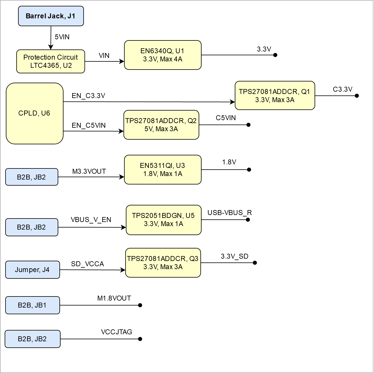
The TEB0707 is quipped with an Intel Max10 as CPLD with the ability of Levelshifting of used for levelshifting of 3.3V signals on CRUVI connectors, JTAG/UART forward to modules, Module control pis, power sequencing and IO voltage selection along with providing User Push buttons, LEDs and switches. For complete information, please see the TEB0707 MAX10 CPLD.
...
| Scroll Title |
|---|
| anchor | Table_OBP_FT2232H |
|---|
| title | FTDI chip interfaces and pins |
|---|
|
| Scroll Table Layout |
|---|
| orientation | portrait |
|---|
| sortDirection | ASC |
|---|
| repeatTableHeaders | default |
|---|
| sortByColumn | 1 |
|---|
| sortEnabled | false |
|---|
| cellHighlighting | true |
|---|
|
| Pin | Schematic | Connected to | Notes |
|---|
| ADBUS0 | TCK | FPGA Bank 1B, U6 | JTAG interface | | ADBUS1 | TDI | FPGA Bank 1B, U6 | | ADBUS2 | TDO | FPGA Bank 1B, U6 | | ADBUS3 | TMS | FPGA Bank 1B, U6 | | BDBUS0 | F_UART_TX | FPGA Bank 1B, U6 | UART Transmitter output | | BDBUS1 | F_UART_RX | FPGA Bank 1B, U6 | UART Receiver Input | | OSCI | OSCI | Oscillator, U7 | Clock 12 MHz | | EECS | EECS | EEPROM, U10 | EEPROM Contains FTDI configuration | | EECLK | EECLK | EEPROM, U10 | | EEDATA | EEDATA | EEPROM, U10 | | DM/DP | FD_N/ FD_P | Micro USB, J15 | USB to UART | | nRESET | 3.3V | 3.3V |
|
...
LEDs
The functions of the LEDs are MAX10 Firmware dependent. See TEB0707 MAX10 CPLD LEDs.
| Scroll Title |
|---|
| anchor | Table_OBP_LED |
|---|
| title | On-board LEDs |
|---|
|
| Scroll Table Layout |
|---|
| orientation | portrait |
|---|
| sortDirection | ASC |
|---|
| repeatTableHeaders | default |
|---|
| style | |
|---|
| widths | |
|---|
| sortByColumn | 1 |
|---|
| sortEnabled | false |
|---|
| cellHighlighting | true |
|---|
|
| Designator | Color | Schematic | Connected to | Active Level | Note |
|---|
| D2D1 | Greengreen | LED3 | FPGA Bank 38 | Active High |
| | D3D2 | Greengreen | LED5 | FPGA Bank 38 | Active High |
| | D4D3 | Greengreen | LED7 | FPGA Bank 38 | Active High |
| | D5D4 | Greenred | LED4 | FPGA Bank 83 | Active High |
| | D6D5 | Greenred | LED6 | FPGA Bank 2 | Active High |
| | D7D6 | Greenred | LED8 | FPGA Bank 8 | Active High |
| | D8D7 | Greenred | LED2 | FPGA Bank 83 | Active High |
| | D9D8 | Greengreen | LED1 | FPGA Bank 83 | Active High |
|
|
EEPROM
The EEPROM IC, U8 contains the FTDI configuration and is prprogrammed with Xilinx JTAG licence.
| Scroll Title |
|---|
| anchor | Table_OBP_EEP |
|---|
| title | I2C EEPROM interface MIOs and pins |
|---|
|
| Scroll Table Layout |
|---|
| orientation | portrait |
|---|
| sortDirection | ASC |
|---|
| repeatTableHeaders | default |
|---|
| style | |
|---|
| widths | |
|---|
| sortByColumn | 1 |
|---|
| sortEnabled | false |
|---|
| cellHighlighting | true |
|---|
|
| Pin | Schematic | Connected to | Notes |
|---|
| CS | EECS | FTDI, U8 |
| | CLK | EECLK | FTDI, U8 |
| | DIN | EEDATA | FTDI, U8 |
|
|
...
There is a DIP Switch provided for direct user controlling and setting of boot mode, programming mode, enable and JTAG selectionuser controlling of settings. Dip1..3 are connected to MAX10 CPLD and therefore function is Firmware dependent, see TEB0707 MAX10 Dips.
| Scroll Title |
|---|
| anchor | Table_OBP_DIP |
|---|
| title | DIP Switch connections |
|---|
|
| Scroll Table Layout |
|---|
| orientation | portrait |
|---|
| sortDirection | ASC |
|---|
| repeatTableHeaders | default |
|---|
| style | |
|---|
| widths | |
|---|
| sortByColumn | 1 |
|---|
| sortEnabled | false |
|---|
| cellHighlighting | true |
|---|
|
| Pin | Schematic | Function (in standard Firmware) | Notes |
|---|
| DIP1 | DIP1 | Forwarded to IO so SoM | MAX10 firmware dependent. | | DIP2 | DIP2 | IO Voltage selection | 1.8V ('high', open, OFF), 2.5V ('low', closed, ON) | | DIP3 | DIP3 (PROGMODE) | Programming mode (JTAG selection on Trenz 4x5 module) | Select between | PROGMODE | Programming mode | select between CPLD (low, closed, on) on SoM or FPGA/SoC (high, open, off ) | | DIP2 | MODE | Boot Mode | select SD boot mode when card installed ('low'), else QSPI ('high') | | DIP3 | EN1 | Power Enable | module power always enabled | OFF ) or CPLD (low, closed, ON), MAX10 firmware dependent.
| | DIP4 | JTAGEN | DIP4 | TAGEN | JTAG Selection | JTAG mode between CPLD (high, closed, ON) or SoM (low, open, OFF) |
|
Push Buttons
Buttons are connected MAX10 CPLD and therefore function is Firmware dependent, see TEB0707 MAX10 CPLD Buttons
| Scroll Title |
|---|
| anchor | Table_OBP_BTN |
|---|
| title | Push Buttons informations |
|---|
|
| Scroll Table Layout |
|---|
| orientation | portrait |
|---|
| sortDirection | ASC |
|---|
| repeatTableHeaders | default |
|---|
| style | |
|---|
| widths | |
|---|
| sortByColumn | 1 |
|---|
| sortEnabled | false |
|---|
| cellHighlighting | true |
|---|
|
| Designator | Schematic | Function (in standard Firmware) | Notes |
|---|
| S2 | RESET | SoM Reset | Hardware debounced. | | S3 | BUTTON1 | User ButtonButton | debounced in Max10 FPGA |
|
Clock Sources
MEMS U7 Oscillator is nedded for FTDI. It is additionally connectd to MAX 10 FPGA Bank 2 Pin H4 and can be used in custom Firmware.
| Scroll Title |
|---|
| anchor | Table_OBP_CLK |
|---|
| title | Osillators |
|---|
|
| Scroll Table Layout |
|---|
| orientation | portrait |
|---|
| sortDirection | ASC |
|---|
| repeatTableHeaders | default |
|---|
| style | |
|---|
| widths | |
|---|
| sortByColumn | 1 |
|---|
| sortEnabled | false |
|---|
| cellHighlighting | true |
|---|
|
| Designator | Description | Frequency | Note |
|---|
| U7 | MEMS OschilatorOscillator | 12 MHz |
|
|
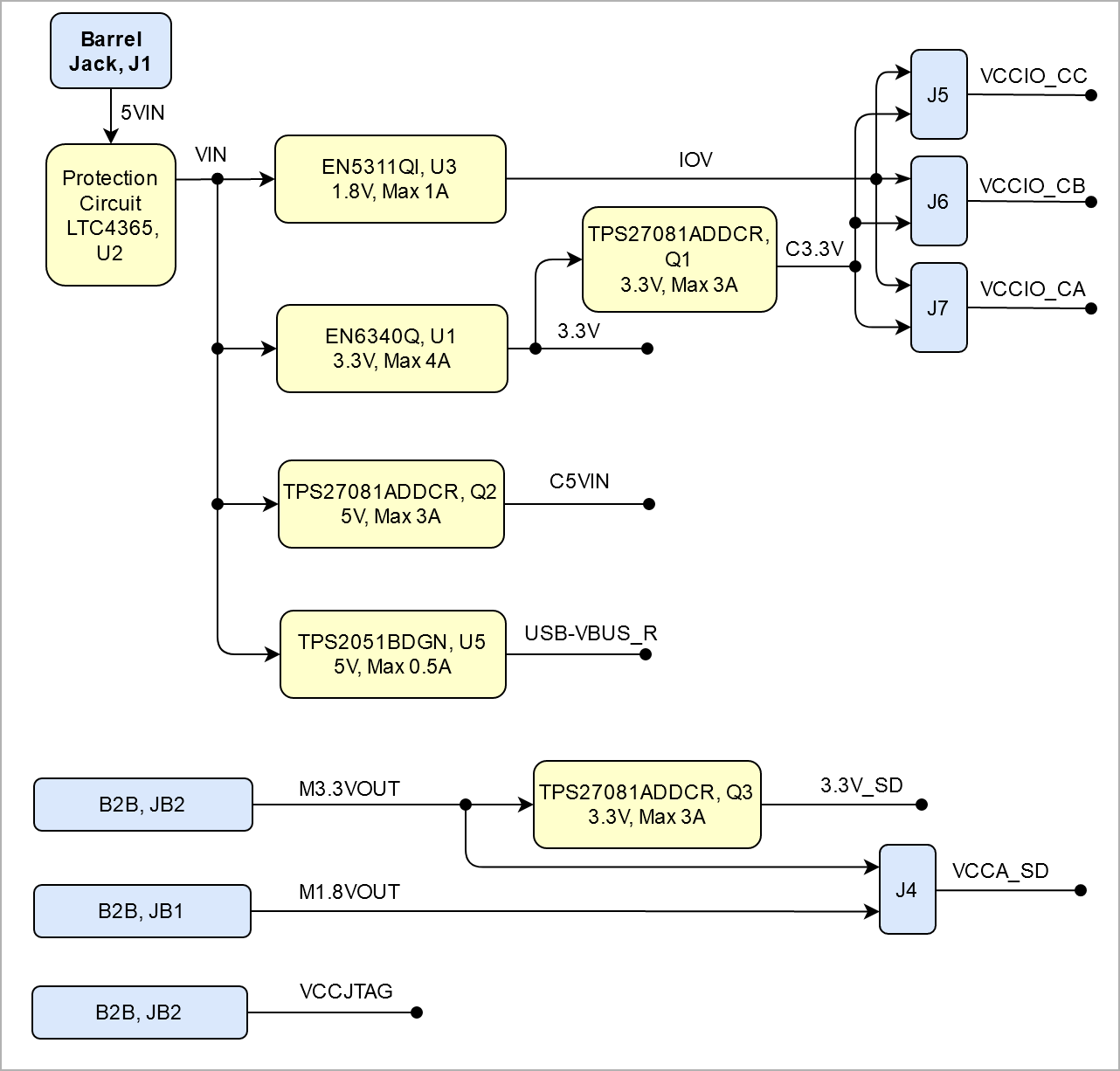
Power and Power-On Sequence
...
Power supply with minimum current capability of xx 3 A for system startup is recommended.
...
| Scroll Title |
|---|
| anchor | Figure_PWR_PD |
|---|
| title | Power Distribution |
|---|
|
| draw.io Diagram |
|---|
| border | false |
|---|
| |
|---|
| diagramName | TEB0707_PWR_DP |
|---|
| simpleViewer | false |
|---|
| width | 639 |
|---|
| links | auto |
|---|
| tbstyle | hidden |
|---|
| diagramDisplayName | |
|---|
| lbox | true |
|---|
| diagramWidth | 641 |
|---|
| revision | 45 |
|---|
|
| Scroll Only |
|---|
|
|
Power-On Sequence
| Scroll Title |
|---|
| anchor | Figure_PWR_PS |
|---|
| title | Power Sequency |
|---|
|
| Scroll Ignore |
|---|
| draw.io Diagram |
|---|
| border | false |
|---|
| |
|---|
| diagramName | TEB0707_PWR_PS |
|---|
| simpleViewer | false |
|---|
| width | 639 |
|---|
| links | auto |
|---|
| tbstyle | hidden |
|---|
| diagramDisplayName | |
|---|
| lbox | true |
|---|
| diagramWidth | 641 |
|---|
| revision | 34 |
|---|
|
|
| Scroll Only |
|---|
|
|
Power Rails
| Scroll Title |
|---|
| anchor | Table_PWR_PR |
|---|
| title | Module power rails. |
|---|
|
| Scroll Table Layout |
|---|
| orientation | portrait |
|---|
| sortDirection | ASC |
|---|
| repeatTableHeaders | default |
|---|
| style | |
|---|
| widths | |
|---|
| sortByColumn | 1 |
|---|
| sortEnabled | false |
|---|
| cellHighlighting | true |
|---|
|
| Power Rail Name | B2B Connector JB1 Pin | B2B Connector JB2 Pin | B2B Connector JB3 Pin | Direction | Notes |
|---|
ETH-VCC | 13| VCCIO_CA | - | 8, 10 | - | Output |
| | VCCIO_CB | - | 2, 4, 6 | - |
Input| Output |
| | VCCIO_CC | 10, 12 | - | - | Output |
M1.8VOUT | 40 | - | - | Input | 14, 16 | - | - | Output | VCCIO_CA8, 10 | VCCIO_CB | - | 2, 4, 6Output| Input |
| | M3.3VOUT | - | 9, 11 | - | Input |
| | ETH-VCC | 13 | - | - | Input |
|
|
Bank Voltages
Below MAX10 CPLD Bankvoltages are summarized.
| Scroll Title |
|---|
| anchor | Table_PWR_BV |
|---|
| title | Zynq SoC bank voltages. |
|---|
|
| Scroll Table Layout |
|---|
| orientation | portrait |
|---|
| sortDirection | ASC |
|---|
| repeatTableHeaders | default |
|---|
| style | |
|---|
| widths | |
|---|
| sortByColumn | 1 |
|---|
| sortEnabled | false |
|---|
| cellHighlighting | true |
|---|
|
| Schematic Name | | Notes |
|---|
| Bank 1A | 3.3V | 3.3V |
| | Bank 1B | 3.3V | 3.3V |
| | Bank 2 | 3.3V | 3.3V |
| | Bank 3 | 3.3V | 3.3V |
| | Bank 5 | VCCJTAG | 3.3VComes |
| from moduleSoM | | Bank 6 | VCCIO_CC | 3.3V/1.8V |
| Variable | | Bank 8 | 3.3V | 3.3V |
|
|
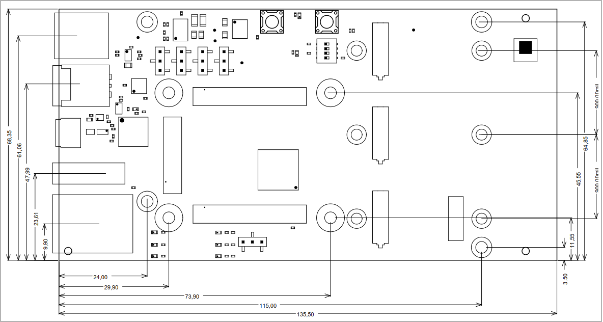
Board to Board Connectors
...
| Scroll Title |
|---|
| anchor | Figure_TS_PD |
|---|
| title | Physical Dimension |
|---|
|
| Scroll Ignore |
|---|
| draw.io Diagram |
|---|
| border | false |
|---|
| |
|---|
| diagramName | TEB0707_TS_PD |
|---|
| simpleViewer | false |
|---|
| width | 639 |
|---|
| links | auto |
|---|
| tbstyle | hidden |
|---|
| diagramDisplayName | |
|---|
| lbox | true |
|---|
| diagramWidth | 641591 |
|---|
| revision | 67 |
|---|
|
|
| Scroll Only |
|---|
| scroll-pdf | true |
|---|
| scroll-office | true |
|---|
| scroll-chm | true |
|---|
| scroll-docbook | true |
|---|
| scroll-eclipsehelp | true |
|---|
| scroll-epub | true |
|---|
| scroll-html | true |
|---|
| 
|
|
...
| Scroll Title |
|---|
| anchor | Table_RH_HRH |
|---|
| title | Hardware Revision History |
|---|
|
| Scroll Table Layout |
|---|
| orientation | portrait |
|---|
| sortDirection | ASC |
|---|
| repeatTableHeaders | default |
|---|
| style | |
|---|
| widths | |
|---|
| sortByColumn | 1 |
|---|
| sortEnabled | false |
|---|
| cellHighlighting | true |
|---|
|
| Date | Revision | Changes | Documentation Link |
|---|
| 2020-11-20 | REV02 | first production release | REV02 | | 2020-04-01 | REV01 | Initial ReleasePrototypes | REV01- |
|
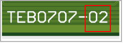
Hardware revision number can be found on the PCB board together with the module model number separated by the dash.
| Scroll Title |
|---|
| anchor | Figure_RV_HRN |
|---|
| title | Board hardware revision number. |
|---|
|
| Scroll Ignore |
|---|
| draw.io Diagram |
|---|
| border | false |
|---|
| |
|---|
| diagramName | TEB0707_RV_HRN |
|---|
| simpleViewer | false |
|---|
| width | 200 |
|---|
| links | auto |
|---|
| tbstyle | hidden |
|---|
| diagramDisplayName | |
|---|
| lbox | true |
|---|
| diagramWidth | 142121 |
|---|
| revision | 56 |
|---|
|
|
| Scroll Only |
|---|
|
|
Document Change History
...