| Page properties |
|---|
|
- Module: TRM Name always "TE Series Name" +TRM
Example: "TE0728 TRM"
Template Change history: | Date | Version | Changes | Author |
|---|
| 3.12 | - Version History
- changed from list to table
- all
- changed title-alignment for tables from left to center
| ma |
| 3.11 | - update "Recommended Operating Conditions" section
|
|
| 3.1 | - New general notes for temperature range to "Recommended Operating Conditions"
|
|
| 3.02 | - add again fix table of content with workaround to use it for pdf and wiki
- Export Link for key features examples
- Notes for different Types (with and without Main FPGA)
- Export Link for Signals, Interfaces and Pins examples
- Notes for different Types (Modul, Modul Hypride, Evalboard, Carrier)
|
|
| 3.01 | - remove fix table of content and page layout ( split page layout make trouble with pdf export)
- changed and add note to signal and interfaces, to on board periphery section
- ...(not finished)
|
|
| 3.00 | - → separation of Carrier/Module and evaluation kit TRM
|
|
| 2.15 | - add excerpt macro to key features
|
|
| 2.14 | - add fix table of content
- add table size as macro
|
|
|
| Page properties |
|---|
|
Important General Note:
|
| Page properties |
|---|
|
----------------------------------------------------------------------- |
| Page properties |
|---|
|
Note for Download Link of the Scroll ignore macro: |
Overview
The Trenz Electronic TE0xxx-xx ... AM0010 module is an industrial/extended grade ... module ... based on AMD Xilinx/Intel...
Refer to http://trenz.org/tec0850am0010-info for the current online version of this manual and other available documentation.
Key Features
| Excerpt |
|---|
- SoC/FPGA
- Device: ZU1 / ZU2 / ZU3 / ZU4 / ZU5 1)
- Engine: CG / EG / EV 1)
- Speedgrade: -1 / -2 1)
- Temperature Range: Extended / Industrial 1)
- Package: SFVC784...
- RAM/Storage
- On Board
- Interface
- Power
- Dimension
- Notes
|
Block Diagram
| Page properties |
|---|
|
add drawIO object in Scroll Ignore section and add reference image in Scroll Only.
| Note |
|---|
Title (not anchor) of all Scroll Title such as DrawIOs and Tables should be changed according to the Module name. Example: TE0812 Block Diagram |
| Note |
|---|
All created DrawIOs should be named according to the Module name: Example: DrawIO of TE0812 Block Diagram should be named TE0812_OV_BD |
- 4 GByte DDR4 SDRAM with ECC 2)
- 8 GByte e.MMC 3)
- Optional HyperFlash 4)
- 2 x 64 MByte Serial Flash 5)
- EEPROM with MAC address
- On Board
- Gigabit Ethernet Transceiver
- USB Transceiver
- OPTIGA Trust M
- CryptoAuthentication
- Oscillator
- Analog Multiplexer
- Interface
- 2 x B2B Connector (ADM6)
up to 204 PL IO up to 22 PS MIO - 4 GTR
- 4 GTH (with ZU4 and higher)
- ETH, USB, I2C, JTAG, ...
- Power
- 5 V ... 12 V power supply via B2B Connector needed.
- Dimension
- Notes
1) Please, take care of the possible assembly options. Furthermore, check whether the power supply is powerful enough for your FPGA design.
2) Up to 32 GByte are possible with a maximum bandwidth of 2400 MBit/s.
3) Up to 64 GByte are possible.
4) Up to 64 MByte are possible.
5) Up to 2 x 256 MByte are possible.
|
Block Diagram
| Scroll Title |
|---|
| anchor | Figure_OV_BD |
|---|
| title-alignment | center |
|---|
| title | TExxxx block diagram |
|---|
|
| Scroll Ignore |
|---|
Create DrawIO object here: Attention if you copy from other page, objects are only linked. |
| Scroll Only |
|---|
image link to the generate DrawIO PNG file of this page. This is a workaround until scroll pdf export bug is fixed |
Main Components
| Page properties |
|---|
|
Notes : Picture of the PCB (top and bottom side) with labels of important componentsAdd List belowadd drawIO object in Scroll Ignore section and add reference image in Scroll Only.
| Note |
|---|
Title (not anchor) of all Scroll Title such as DrawIOs and Tables should be changed according to the Module name. Example: TE0812 Block Diagram |
| Note |
|---|
All created DrawIOs should be named according to the Module name: Example: DrawIO of TE0812 Block Diagram should be named TE0812_OV_BD |
|
| Scroll Title |
|---|
|
| Scroll Title |
|---|
| anchor | Figure_OV_MC |
|---|
| title-alignment | center |
|---|
| title | TExxxx main componentsAM0010 block diagram |
|---|
|
| Scroll Ignore |
|---|
Create DrawIO object here: Attention if you copy from other page, objects are only linked. |
| Scroll Only |
|---|
image link to the generate DrawIO PNG file of this page. This is a workaround until scroll pdf export bug is fixed |
|
- ...
- ...
- ...
Initial Delivery State| draw.io Diagram |
|---|
| border | true |
|---|
| |
|---|
| diagramName | AM0010_OV_BD |
|---|
| simpleViewer | true |
|---|
| width | |
|---|
| links | auto |
|---|
| tbstyle | top |
|---|
| diagramDisplayName | |
|---|
| lbox | true |
|---|
| diagramWidth | 691 |
|---|
| revision | 7 |
|---|
|
|
| Scroll Only |
|---|
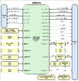 Image Added Image Added
|
|
Main Components
| Page properties |
|---|
| | Note |
|---|
Only components like EEPROM, QSPI flash can be initialized by default at manufacture. If there is no components which might have initial data ( possible on carrier) you must keep the table empty |
Notes : - Picture of the PCB (top and bottom side) with labels of important components
- Add List below
|
| Scroll Title |
|---|
|
| Scroll Title |
|---|
| anchor | Table_OV_IDS |
|---|
| title-alignment | center |
|---|
| title | Initial delivery state of programmable devices on the moduleAM0010 main components |
|---|
|
tablelayoutorientationportrait |
| sortDirection | ASC |
|---|
| repeatTableHeaders | default |
|---|
style | widths | | sortByColumn | 1 |
|---|
| sortEnabled | false |
|---|
| cellHighlighting | true |
|---|
Storage device name | Content | Notes |
|---|
Quad SPI Flash | EEPROM | System Controller CPLD | DDR4 SDRAM | eMMC | Programmable Clock Generator |
Configuration Signals
| Page properties |
|---|
|
- Overview of Boot Mode, Reset, Enables.
|
| |
|---|
| diagramName | Figure_OV_MC |
|---|
| simpleViewer | true |
|---|
| width | |
|---|
| links | auto |
|---|
| tbstyle | top |
|---|
| diagramDisplayName | |
|---|
| lbox | true |
|---|
| diagramWidth | 720 |
|---|
| revision | 3 |
|---|
|
|
| Scroll Only |
|---|
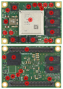 Image Added Image Added
|
|
- FPGA, U1
- DDR4, U2, U3, U9, U12, U14
- eMMC, U17
- Quad SPI Flash, U6, U7
- Connector, J5, J6
- Ethernet Transceiver, U8
- HyperFlash, U16
- EEPROM, U15
- OPTIGA Trust M, U27
- CryptoAuthentication, U24
- USB Transceiver, U10
- Oscillator, U13, U14, U30, U31, U32
- Analog Multiplexer, U38
- Power Supply, U5, U11, U18, U19, U20, U21, U22, U23, U28
Initial Delivery State
| Page properties |
|---|
|
| Note |
|---|
Only components like EEPROM, QSPI flash can be initialized by default at manufacture. If there is no components which might have initial data ( possible on carrier) you must keep the table empty |
|
| Scroll Title |
|---|
| anchor | Table_OV_IDS |
|---|
| title-alignment | center |
|---|
| title | Initial delivery state of programmable devices on the module |
|---|
|
|
| Scroll Title |
|---|
| anchor | Table_OV_CNTRL |
|---|
| title-alignment | center |
|---|
| title | Controller signal. |
|---|
|
| Scroll Table Layout |
|---|
| orientation | portrait |
|---|
| sortDirection | ASC |
|---|
| repeatTableHeaders | default |
|---|
| style | |
|---|
| widths | |
|---|
| sortByColumn | 1 |
|---|
| sortEnabled | false |
|---|
| cellHighlighting | true |
|---|
|
Storage device name | Content | Notes |
|---|
| DDR4 SDRAM | not programmed |
| | eMMC | not programmed |
| | Quad SPI Flash | not programmed |
| HyperFlash | not programmed |
| | EEPROM | not programmed besides factory programmed MAC address |
Name | B2B/Connector | Direction | Description |
|---|
Boot Mode | Enable | Reset | JTAGSEL | PGOOD | ...
|
Signals, Interfaces and Pins
B2B SoC/FPGA IOs
B2B JTAG Interface
B2B ETH Interface
B2B USB Interface
SD Card Connector
SMA Connector
MIO
| Page properties |
|---|
|
| Note |
|---|
|
MIO section only for SoC devices with dedicated MIO, otherwhise remove this section |
MIO Pins
| Page properties |
|---|
|
Only for SoC Modules(Xilinx MIO, for Intel and MicroChip SoC please change MIO to syntax of the manufacturer). you must fill the table below with group of MIOs which are connected to a specific components or peripherals, you do not have to specify pins in B2B, Just mention which B2B is connected to MIOs. The rest is clear in the Schematic.
MIO Pins are only for SoC like Zynq, U+Zynq and Versal, for other FPGA modules remove this chapter
Example:
- Table with all connectors and Designtor
- List of different interfaces per connector
- IO CNT (for FPGA IOs where functionality can be changed by customer)
|
|
Connectors
| Scroll Title |
|---|
| anchor | Table_SIP_C |
|---|
| title-alignment | center |
|---|
| title | Board Connectors |
|---|
|
| Scroll Table Layout |
|---|
| orientation | portrait |
|---|
| sortDirection | ASC |
|---|
| repeatTableHeaders | default |
|---|
| style | |
|---|
| widths | |
|---|
| sortByColumn | 1 |
|---|
| sortEnabled | false |
|---|
| cellHighlighting | true |
|---|
|
| Connector Type | Designator | Interface | IO CNT 1) | Notes |
|---|
| B2B | J5 | HP | 104 SE / 48 DIFF |
| | B2B | J5 | MGT PL | 4 x MGT (RX/TX) |
| | B2B | J5 | MGT PL | 2 x MGT CLK |
| | B2B | J5 | HD | 24 SE / 12 DIFF |
| | B2B | J6 | HP | 52 SE / 24 DIFF |
| | B2B | J6 | MGT PS | 4 x MGT (RX/TX) |
| | B2B | J6 | MGT PS | 2 x MGT CLK |
| | B2B | J6 | HD | 24 SE / 12 DIFF |
| | B2B | J6 | MIO | 2 x I2C |
| | B2B | J6 | MIO | 2 x UART |
| | B2B | J6 | MIO | 2 x PERST |
| | B2B | J6 | MIO | SDIO |
| | B2B | J6 | MIO | JTAG |
| | B2B | J6 | MIO | 4 x GPIO |
| | B2B | J6 | ETH |
|
| | B2B | J6 | USB |
|
|
1) IO CNT depends on assembly variant. E.g. the MGTs are not available for all FPGAs |
Test Points
| Page properties |
|---|
|
you must fill the table below with group of Test Point which are indicated as TP in a schematic. If there is no Test Point remarked in the schematic, delet the Test Point section. Example: | Test Point | Signal | B2B | Notes |
|---|
| 10 | PWR_PL_OK | J2-120 |
|
|
| Scroll Title |
|---|
| anchor | Table_SIP_TPs |
|---|
| title-alignment | center |
|---|
| title | Test Points Information |
|---|
|
| MIO Pin | Connected to | B2B | Notes |
|---|
| MIO12...14 | SPI_CS , SPI_DQ0... SPI_DQ3 SPI_SCK | J2 | QSPI |
Test Points
| Page properties |
|---|
|
you must fill the table below with group of Test Point which are indicated as TP in a schematic. If there is no Test Point remarked in the schematic, delet the Test Point section.
Example:
| Test Point | Signal | B2B | Notes |
|---|
10 | PWR_PL_OK | J2-120 | | Scroll Title |
|---|
| anchor | Table_SIP_TPs |
|---|
| title-alignment | center |
|---|
| title | Test Points Information |
|---|
|
| Scroll Table Layout |
|---|
| orientation | portrait |
|---|
| sortDirection | ASC |
|---|
| repeatTableHeaders | default |
|---|
style | widths | | sortByColumn | 1 |
|---|
| sortEnabled | false |
|---|
| cellHighlighting | true |
|---|
| Test Point | Signal | Connected to | Notes |
|---|
TP1 | TP2 | TP3 | TP4 | TP5 | TP6 | TP7 | TP8 | TP9 | TP10 | On-board Peripherals
| Page properties |
|---|
|
Notes : In the on-board peripheral table "chip/Interface" must be linked to the corresponding chapter or subsection by assigning advance link using: #NameOfTheSection Example: #ClockSources, #CPLD, #QuadSPIFlash |
Power and Power-On Sequence
| Page properties |
|---|
|
In 'Power and Power-on Sequence' section there are three important digrams which must be drawn:
- Power on-sequence
- Power distribution
- Voltage monitoring circuit
| PROG_B# | pulled-up to V_IO_CFG | | TP2 | VTT |
| | TP3 | VTT |
| | TP4 | VREFA |
| | TP5 | VREFA |
| | TP6 | 0.85V |
| | TP7 | 0.85V |
| | TP8 | DDR_1V2 |
| | TP9 | DDR_1V2 |
| | TP10 | MGTAVCC |
| | TP11 | MGTAVCC |
| | TP12 | DDR_2V5 |
| | TP13 | DDR_2V5 |
| | TP14 | PL_VCU_0V9 |
| | TP15 | PL_VCU_0V9 |
| | TP16 | 1.8V |
| | TP17 | 1.8V |
| | TP18 | 3.3V_SEQ |
| | TP19 | 3.3V_SEQ |
| | TP20 | 3.3V |
| | TP21 | 3.3V |
|
|
On-board Peripherals
| Page properties |
|---|
|
Notes : In the on-board peripheral table "chip/Interface" must be linked to the corresponding chapter or subsection by assigning advance link using: #NameOfTheSection Example: | Chip/Interface | Designator | Connected To | Notes |
|---|
| ETH PHY | U10 | | Gigabit ETH PHY |
|
Power Supply
Power supply with minimum current capability of xx A for system startup is recommended.
Power Consumption
| Scroll Title |
|---|
| anchor | Table_PWR_PC |
|---|
| title-alignment | center |
|---|
| title | Power Consumption |
|---|
|
| Scroll Table Layout |
|---|
| orientation | portrait |
|---|
| sortDirection | ASC |
|---|
| repeatTableHeaders | default |
|---|
style | widths | | sortByColumn | 1 |
|---|
| sortEnabled | false |
|---|
| cellHighlighting | true |
|---|
| Power Input Pin | Typical Current |
|---|
| VIN | TBD* |
* TBD - To Be Determined
Power Distribution Dependencies
| Scroll Title |
|---|
| anchor | FigureTable_PWR_PDOBP |
|---|
| title-alignment | center |
|---|
| title | Power DistributionOn board peripherals |
|---|
|
| ignore |
Create DrawIO object here: Attention if you copy from other page, objects are only linked. |
| Scroll Only |
|---|
image link to the generate DrawIO PNG file of this page. This is a workaround until scroll pdf export bug is fixed |
Power-On Sequence
| Scroll Title |
|---|
| anchor | Figure_PWR_PS |
|---|
| title-alignment | center |
|---|
| title | Power Sequency |
|---|
|
| Scroll Ignore |
|---|
Create DrawIO object here: Attention if you copy from other page, objects are only linked. |
| Scroll Only |
|---|
image link to the generate DrawIO PNG file of this page. This is a workaround until scroll pdf export bug is fixed |
| tablelayout |
|---|
| orientation | portrait |
|---|
| sortDirection | ASC |
|---|
| repeatTableHeaders | default |
|---|
| style | |
|---|
| widths | |
|---|
| sortByColumn | 1 |
|---|
| sortEnabled | false |
|---|
| cellHighlighting | true |
|---|
|
| Chip/Interface | Designator | Connected To | Notes |
|---|
DDR4 SDRAM | U2, U3, U9, U12, U14 | SoC - PS |
| eMMC | U17 | SoC - PS |
| Quad SPI Flash | U6, U7 | SoC - PS | Booting. | Gigabit Ethernet Transceiver | U8 | SoC - PS |
| HyperFlash | U16 | SoC - PL |
| EEPROM | U15 | SoC - PS |
| OPTIGA Trust M | U27 | SoC - PS |
| CryptoAuthentication | U24 | SoC - PS |
| USB 2 Transceiver | U10 | SoC - PS |
| Oscillator | U13 | SoC - PS | 135 MHz | Oscillator | U14 | SoC - PS | 100 MHz | Oscillator | U30 | ETH PHY | 25 MHz | Oscillator | U31 | USB PHY | 24 MHz | Oscillator | U32 | SoC | 33 MHz | Analog Multiplexer | U38 | SoC | Voltage measuring with Xilinx internal ADC. |
|
Configuration and System Control Signals
| Page properties |
|---|
|
- Overview all Controller signals, like Reset, Boote Mode, JTAG Interface(Connector or USB In case of FTDI)...
- In case it's connected to CPLD always link to CPLD description and add not from the current implementation here(in case it's available)
|
| Scroll Title |
|---|
| anchor | Table_OV_CNTRL |
|---|
| title-alignment | center |
|---|
| title | Controller signal. |
|---|
|
| Scroll Table Layout |
|---|
| orientation | portrait |
|---|
| sortDirection | ASC |
|---|
| repeatTableHeaders | default |
|---|
| style | |
|---|
|
|
Voltage Monitor Circuit
| Scroll Title |
|---|
| anchor | Figure_PWR_VMC |
|---|
| title-alignment | center |
|---|
| title | Voltage Monitor Circuit |
|---|
|
| Scroll Ignore |
|---|
Create DrawIO object here: Attention if you copy from other page, objects are only linked. |
| Scroll Only |
|---|
image link to the generate DrawIO PNG file of this page. This is a workaround until scroll pdf export bug is fixed |
Power Rails
| Scroll Title |
|---|
| anchor | Table_PWR_PR |
|---|
| title-alignment | center |
|---|
| title | Module power rails. |
|---|
|
| Scroll Table Layout |
|---|
| orientation | portrait |
|---|
| sortDirection | ASC |
|---|
| repeatTableHeaders | default |
|---|
style | widths | | sortByColumn | 1 |
|---|
| sortEnabled | false |
|---|
| cellHighlighting | true |
|---|
| Power Rail Name | B2B Connector JM1 Pin | B2B Connector JM2 Pin | B2B Connector JM3 Pin | Direction | Notes |
|---|
Bank Voltages
| Scroll Title |
|---|
| anchor | Table_PWR_BV |
|---|
| title-alignment | center |
|---|
| title | Zynq SoC bank voltages. |
|---|
|
| Scroll Table Layout |
|---|
| orientation | portrait |
|---|
| sortDirection | ASC |
|---|
| repeatTableHeaders | default |
|---|
style | widths | | sortByColumn | 1 |
|---|
| sortEnabled | false |
|---|
| cellHighlighting | true |
|---|
| Schematic Name | | Notes |
|---|
Board to Board Connectors| Page properties |
|---|
|
This section is optional and only for modules.use "include page" macro and link to the general B2B connector page of the module series,
For example: 6 x 6 SoM LSHM B2B Connectors| Include Page |
|---|
PD:6 x 6 SoM LSHM B2B Connectors | PD:6 x 6 SoM LSHM B2B Connectors | Technical Specifications
Absolute Maximum Ratings
| Scroll Title |
|---|
| anchor | Table_TS_AMR |
|---|
| title-alignment | center |
|---|
| title | PS absolute maximum ratings |
|---|
|
| Scroll Table Layout |
|---|
| orientation | portrait |
|---|
| sortDirection | ASC |
|---|
| repeatTableHeaders | default |
|---|
| style | widths | |
|---|
| sortByColumn | 1 |
|---|
| sortEnabled | false |
|---|
| cellHighlighting | true |
|---|
|
|
| Symbols | Description | Min | Max | Unit |
|---|
V | V | V | V | V | V | V | V | °C |
Recommended Operating Conditions
This TRM is generic for all variants. Temperature range can be differ depending on the assembly version. Voltage range is mostly the same during variants (exceptions are possible, depending on custom request)
Operating temperature range depends also on customer design and cooling solution. Please contact us for options.
- Variants of modules are described here: Article Number Information
- Modules with commercial temperature grade are equipped with components that cover at least the range of 0°C to 75°C
- Modules with extended temperature grade are equipped with components that cover at least the range of 0°C to 85°C
- Modules with industrial temperature grade are equipped with components that cover at least the range of -40°C to 85°C
- The actual operating temperature range will depend on the FPGA / SoC design / usage and cooling and other variables.
| Scroll Title |
|---|
| anchor | Table_TS_ROC |
|---|
| title-alignment | center |
|---|
| title | Recommended operating conditions. |
|---|
|
| Scroll Table Layout |
|---|
| orientation | portrait |
|---|
| sortDirection | ASC |
|---|
| repeatTableHeaders | default |
|---|
style | widths | | sortByColumn | 1 |
|---|
| sortEnabled | false |
|---|
| cellHighlighting | true |
|---|
| Parameter | Min | Max | Units | Reference Document |
|---|
V | See ???? datasheets. | V | See ???? datasheet. | V | See ???? datasheet. | V | See ???? datasheet. | V | See ???? datasheet. | V | See ???? datasheet. | V | See ???? datasheet. | °C | See ???? datasheet. | Physical Dimensions
PCB thickness: ?? mm.
| Page properties |
|---|
|
In 'Physical Dimension' section, top and bottom view of module must be inserted, information regarding physical dimensions can be obtained through webpage for product in Shop.Trenz, (Download> Documents> Assembly part) for every SoM.
For Example: for Module TE0728, Physical Dimension information can be captured by snipping tools from the link below:
https://www.trenz-electronic.de/fileadmin/docs/Trenz_Electronic/Modules_and_Module_Carriers/5.2x7.6/TE0745/REV02/Documents/AD-TE0745-02-30-1I.PDF
| Connector.Pin | Signal Name | Direction1) | Description |
|---|
| J6.A59 | V_BAT | IN | Input voltage for VCC_PSBATT 2) 3). | | J6.B58 | RST_M2C# | OUT | Module reset for baseboard peripheral. | | J6.C53 | DONE | OUT | Signal PS_DONE 2). | | J6.C54 / J6.C55 / J6.C56 / J6.C57 | MODE0..3 | IN | Boot mode selection 2):
- JTAG
- QUAD-SPI (32 Bit)
- SD1 (2.0)
- eMMC (1.8 V)
- SD1 LS (3.0)
Supported Modes depends also on used Carrier. | | J6.C58 | PS_SRST# | IN | SoC Soft Reset 2). | | J6.C59 | PS_POR# | IN | SoC Power-on-reset 2). PWR_GOOD deasserts module reset. | | J6.D56 / J6.D57 | DX_P / DX_N | IN | Temperature sensing diode pin. When not used, tie to GND. | | J6.D58 | PWR_EN | IN / OUT | Power Enable. Controlled module internally. Can be used to delay power on sequencing or disable power. Tie only to GND or leave floating.
| | J6.D59 | PWR_GOOD | OUT | Power good status. | | J6.D51 / J6.D52 / J6.D54 / J6.D55 | TDI/TCK/TDO/TMS | Signal-dependent | JTAG configuration and debugging interface. JTAG reference voltage: V_IO_CFG | | LED D1 / D2 | ERR_STATUS / ERR_OUT | --- | PS_STATUS_ERROR_OUT / PS_ERROR_OUT 2). |
1) Direction: - IN: Input from the point of view of this board.
- OUT: Output from the point of view of this board.
2) See UG1085 for additional information. 3) See Recommended Operating Conditions. |
Power and Power-On Sequence
| Page properties |
|---|
|
Enter the default value for power supply and startup of the module here. - Order of power provided Voltages and Reset/Enable signals
Link to Schematics, for power images or more details |
Power Rails
| Page properties |
|---|
|
List of all Powerrails which are accessible by the customer - Main Power Rails and Variable Bank Power
|
| Scroll Title |
|---|
| anchor | Table_PWR_PR |
|---|
| title-alignment | center |
|---|
| title | Module power rails. |
|---|
|
| Scroll Table Layout |
|---|
| orientation | portrait |
|---|
| sortDirection | ASC |
|---|
| repeatTableHeaders | default |
|---|
| style | |
|---|
| widths | |
|---|
| sortByColumn | 1 |
|---|
| sortEnabled | false |
|---|
| cellHighlighting | true |
|---|
|
| Power Rail Name/ Schematic Name | Connector.Pin | Direction1) | Notes |
|---|
| V_MOD1 | J5.A7 / J5.A15 / J5.A47 / J5.A55 / J5.B5 / J5.B11 / J5.B17 / J5.B45 / J5.B51 / J5.B57 / J6.C5 / J6.C11 / J6.C17 / J6.D7 / J6.D15 | IN |
| | 1.8V | J5.C7 / J5.C15 / J6.B7 / J6.B15 | OUT |
| | V_IO_W01 | J5.D3 / J5.D17 | IN |
| | V_IO_W3 | J5.D40 | IN |
| | V_IO_W45 | J5.D43 / J5.D57 | IN |
| | V_IO_X01 | J6.A3 / J6.A17 | IN |
| | V_BAT | J6.A59 | IN |
| | V_IO_X3 | J6.B35 | IN |
| | 3.3V | J6.B59 | OUT |
| | V_IO_CFG | J6.C52 | IN |
|
1) Direction: - IN: Input from the point of view of this board.
- OUT: Output from the point of view of this board.
|
Recommended Power up Sequencing
| Page properties |
|---|
|
List baseboard design hints for final baseboard development. |
| Scroll Title |
|---|
| anchor | Table_BB_DH |
|---|
| title-alignment | center |
|---|
| title | Baseboard Design Hints |
|---|
|
| Scroll Table Layout |
|---|
| orientation | portrait |
|---|
| sortDirection | ASC |
|---|
| repeatTableHeaders | default |
|---|
| style | |
|---|
| widths | |
|---|
| sortByColumn | 1 |
|---|
| sortEnabled | false |
|---|
| cellHighlighting | true |
|---|
|
| Sequence | Net name | Recommended Voltage Range | Pull-up/down | Description | Notes |
|---|
| 0 | - | - | - | Configuration signal setup. | See Configuration and System Control Signals. | | 1 1) | V_BAT | 3.3 V | - | Battery connection. | Battery Power Domain usage. When not used, tie to GND. | | 2 | V_MOD1 | 12 V | - | Main Power supply. | Main module power supply. 3 A recommended. Power consumption depends mainly on design and cooling solution. | | 3 1) | PWR_EN | - | PU 2), 3.3 V | Power release. | Controlled module internally. Can be used to delay power on sequencing or disable power. Tie only to GND or leave floating. | | 4 | PWR_GOOD | - | PU 2), 3.3 V | Power good status. | Module power on sequencing finished. Periphery and variable bank voltages can be enabled on carrier. | | 5 1) | 3.3V / 1.8V | - | - | Module generated output voltages. | Voltages are available after PWR_GOOD deassertion. These voltages can be used - to supply bank voltages,
- to supply periphery and/or
- as power good signal to enable external power regulators.
Important: Consider maximum power consumption. | | 5 | V_IO_W01 / V_IO_W45 / V_IO_X01 / V_IO_W3 / V_IO_X3 / V_IO_CFG | 3) | - | Module bank voltages. | Enable bank voltages after PWR_GOOD deassertion. To achieve minimum current draw and ensure that the I/Os are 3-stated at power-on it is recommended to enable bank voltages before or at the same time as external logic, | | 6 1) | - | - | - | Reset handling. | RST_M2C# delivers external periphery reset. See Configuration and System Control Signals. |
1) (optional) 2) (on module) 3) See DS925 for additional information. |
Board to Board Connectors
| Page properties |
|---|
|
- This section is optional and only for modules.
use "include page" macro and link to the general B2B connector page of the module series, For example: 6 x 6 SoM LSHM B2B Connectors
| Include Page |
|---|
| https://wiki.trenz-electronic.de/pages/viewpage.action?pageId=139253650&moved=true |
|---|
| https://wiki.trenz-electronic.de/pages/viewpage.action?pageId=139253650&moved=true |
|---|
|
|
| Include Page |
|---|
| Andromeda ADM6/ADF6 B2B Connectors |
|---|
| Andromeda ADM6/ADF6 B2B Connectors |
|---|
|
Technical Specifications
Absolute Maximum Ratings *)
| Scroll Title |
|---|
| anchor | Table_TS_AMR |
|---|
| title-alignment | center |
|---|
| title | AM0010 absolute maximum ratings |
|---|
|
| Scroll Table Layout |
|---|
| orientation | portrait |
|---|
| sortDirection | ASC |
|---|
| repeatTableHeaders | default |
|---|
| style | |
|---|
| widths | |
|---|
| sortByColumn | 1 |
|---|
| sortEnabled | false |
|---|
| cellHighlighting | true |
|---|
|
| Power Rail Name/ Schematic Name | Description | Min | Max | Unit |
|---|
| V_MOD1 | Main input power supply | -0.3 | 18 | V | | V_IO_W01 | HP FPGA Bank 65 voltage | -0.500 | 2.000 | V | | V_IO_W3 | HD FPGA Bank 24 voltage | -0.500 | 3.400 | V | | V_IO_W45 | HP FPGA Bank 64 voltage | -0.500 | 2.000 | V | | V_IO_X01 | HP FPGA Bank 66 voltage | -0.500 | 2.000 | V | | V_BAT 1) | FPGA Battery Voltage |
| 6 | V | | V_IO_X3 | HD FPGA Bank 24 voltage | -0.500 | 3.400 | V | | V_IO_CFG | PS FPGA Bank 501 and 503 Voltage | -0.3 | 3.630 | V |
1) It is possible to use a resistor instead of the LDO but then, consider the different min (-0.500 V) / max (2.000 V) values. |
*) Stresses beyond those listed under Absolute Maximum Ratings may cause permanent damage to the device. These are stress ratings only, which do not imply functional operation of the device at these
or any other conditions beyond those indicated under Recommended Operating Condition. Exposure to absolute-maximum rated conditions for extended periods may affect device reliability.
Recommended Operating Conditions
This TRM is generic for all variants. Temperature range can be differ depending on the assembly version. Voltage range is mostly the same during variants (exceptions are possible, depending on custom request)
Operating temperature range depends also on customer design and cooling solution. Please contact us for options.
- Variants of modules are described here: Article Number Information
- Modules with commercial temperature grade are equipped with components that cover at least the range of 0°C to 75°C
- Modules with extended temperature grade are equipped with components that cover at least the range of 0°C to 85°C
- Modules with industrial temperature grade are equipped with components that cover at least the range of -40°C to 85°C
- The actual operating temperature range will depend on the FPGA / SoC design / usage and cooling and other variables.
| Scroll Title |
|---|
| anchor | Table_TS_ROC |
|---|
| title-alignment | center |
|---|
| title | Recommended operating conditions. |
|---|
|
| Scroll Table Layout |
|---|
| orientation | portrait |
|---|
| sortDirection | ASC |
|---|
| repeatTableHeaders | default |
|---|
| style | |
|---|
| widths | |
|---|
| sortByColumn | 1 |
|---|
| sortEnabled | false |
|---|
| cellHighlighting | true |
|---|
|
| Parameter | Min | Max | Units | Reference Document |
|---|
| V_MOD1 | 4.5 | 16 | V | See TPS54A24 and FS1406 datasheets. | | V_IO_W01 | 0.950 | 1.900 | V | See FPGA datasheet. | | V_IO_W3 | 1.140 | 3.400 | V | See FPGA datasheet. | | V_IO_W45 | 0.950 | 1.900 | V | See FPGA datasheet. | | V_IO_X01 | 0.950 | 1.900 | V | See FPGA datasheet. | | V_BAT 1) | 2.0 | 5.5 | V | See AP7354D datasheet. | | V_IO_X3 | 1.140 | 3.400 | V | See FPGA datasheet. | | V_IO_CFG | 1.710 | 3.465 | V | See FPGA datasheet. |
1) Using a resistor instead of the LDO is possible which leads to different min (1.2 V) / max (1.89 V) values. |
Physical Dimensions
PCB thickness: 2 mm.
| Scroll Title |
|---|
| anchor | Figure_TS_PD |
|---|
| title-alignment | center |
|---|
| title | Physical Dimension |
|---|
|
| Scroll Ignore |
|---|
| draw.io Diagram |
|---|
| border | true |
|---|
| |
|---|
| diagramName | Figure_TS_PD |
|---|
| simpleViewer | false |
|---|
| width | |
|---|
| links | auto |
|---|
| tbstyle | top |
|---|
| lbox | true |
|---|
| diagramWidth | 626 |
|---|
| revision | 2 |
|---|
|
|
| Scroll Only |
|---|
| scroll-pdf | true |
|---|
| scroll-office | true |
|---|
| scroll-chm | true |
|---|
| scroll-docbook | true |
|---|
| scroll-eclipsehelp | true |
|---|
| scroll-epub | true |
|---|
| scroll-html | true |
|---|
|
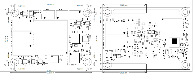 Image Added Image Added
|
|
Currently Offered Variants
| Scroll Title |
|---|
| anchor | Table_VCP_SO |
|---|
| title-alignment | center |
|---|
| title | Trenz Electronic Shop Overview |
|---|
|
| Scroll Table Layout |
|---|
| orientation | portrait |
|---|
| sortDirection | ASC |
|---|
| repeatTableHeaders | default |
|---|
| style | |
|---|
| widths | |
|---|
| sortByColumn | 1 |
|---|
| sortEnabled | false |
|---|
| cellHighlighting | true |
|---|
|
|
Revision History
Hardware Revision History
| Scroll Title |
|---|
| anchor | Figure_TS_PD |
|---|
| title-alignment | center |
|---|
| title | Physical Dimension |
|---|
|
| Scroll Ignore |
|---|
Create DrawIO object here: Attention if you copy from other page, objects are only linked. |
| Scroll Only |
|---|
| scroll-pdf | true |
|---|
| scroll-office | true |
|---|
| scroll-chm | true |
|---|
| scroll-docbook | true |
|---|
| scroll-eclipsehelp | true |
|---|
| scroll-epub | true |
|---|
| scroll-html | true |
|---|
|
image link to the generate DrawIO PNG file of this page. This is a workaround until scroll pdf export bug is fixed |
Currently Offered Variants Revision History
Hardware Revision History
| Scroll Title |
|---|
| anchor | Figure_RV_HRN |
|---|
| title-alignment | center |
|---|
| title | Board hardware revision number. |
|---|
|
| Scroll Ignore |
|---|
| draw.io Diagram |
|---|
| border | true |
|---|
| |
|---|
| diagramName | Figure_RV_HRN |
|---|
| simpleViewer | true |
|---|
| width | |
|---|
| links | auto |
|---|
| tbstyle | top |
|---|
| diagramDisplayName | |
|---|
| lbox | true |
|---|
| diagramWidth | 223 |
|---|
| revision | 1 |
|---|
|
|
| Scroll Only |
|---|
| scroll-viewport | true |
|---|
| scroll-pdf | true |
|---|
| scroll-office | true |
|---|
| scroll-chm | true |
|---|
| scroll-docbook | true |
|---|
| scroll-eclipsehelp | true |
|---|
| scroll-epub | true |
|---|
| scroll-html | true |
|---|
| 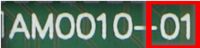 Image Added Image Added
|
|
| Page properties |
|---|
|
Set correct links to download Carrier, e.g. TE0706 REV02:
TE0706-02 -> https://shop.trenz-electronic.de/Download/?path=Trenz_Electronic/Modules_and_Module_Carriers/4x5/4x5_Carriers/TE0706/REV02/Documents
Note:
Date format: YYYY-MM-DDExample:
| Date | Revision | Changes | Documentation Link |
|---|
| 2020-11-25 | REV02 | - Resistors R14 and R15 was replaced by 953R (was 5K1)
- Resistor R5 was replaced by 5K1, R8 by 953R (was 9K09 and 1K69 respectively)
| REV02 |
| Scroll Title |
|---|
| anchor | Figure_RV_HRN |
|---|
| title-alignment | center |
|---|
| title | Board hardware revision number. |
|---|
|
| Scroll Ignore |
|---|
Create DrawIO object here: Attention if you copy from other page, objects are only linked. |
| Scroll Only |
|---|
image link to the generate DrawIO PNG file of this page. This is a workaround until scroll pdf export bug is fixed |
|
| Scroll Title |
|---|
| anchor | Table_RH_HRH |
|---|
| title-alignment | center |
|---|
| title | Hardware Revision History |
|---|
|
| Scroll Table Layout |
|---|
| orientation | portrait |
|---|
| sortDirection | ASC |
|---|
| repeatTableHeaders | default |
|---|
| style | |
|---|
| widths | |
|---|
| sortByColumn | 1 |
|---|
| sortEnabled | false |
|---|
| cellHighlighting | true |
|---|
|
| Date | Revision | Changes | Documentation Link |
|---|
| - | REV01 | First Production Release | REV01 |
|
Hardware revision number can be found on the PCB board together with the module model number separated by the dash.
Document Change History
| Page properties |
|---|
|
- Note this list must be only updated, if the document is online on public doc!
- It's semi automatically, so do following
Add new row below first Copy "Page Information Macro (date)" Macro-Preview, Metadata Version number, Author Name and description to the empty row. Important Revision number must be the same as the Wiki document revision number Update Metadata = "Page Information Macro (current-version)" Preview+1 and add Author and change description. --> this point is will be deleted on newer pdf export template - Metadata is only used of compatibility of older exports
|
| Scroll Title |
|---|
| anchor | Table_RH_DCH |
|---|
| title-alignment | center |
|---|
| title | Document change history. |
|---|
|
| Scroll Table Layout |
|---|
| orientation | portrait |
|---|
| sortDirection | ASC |
|---|
| repeatTableHeaders | default |
|---|
| style | |
|---|
| widths | |
|---|
| sortByColumn | 1 |
|---|
| sortEnabled | false |
|---|
| cellHighlighting | true |
|---|
|
| Date | Revision | Contributor | Description |
|---|
| Page info |
|---|
| infoType | Modified date |
|---|
| dateFormat | yyyy-MM-dd |
|---|
| type | Flat |
|---|
|
| | Page info |
|---|
| infoType | Current version |
|---|
| prefix | v. |
|---|
| type | Flat |
|---|
| showVersions | false |
|---|
|
| | Page info |
|---|
| infoType | Modified by |
|---|
| type | Flat |
|---|
| showVersions | false |
|---|
|
| - Recommended Power up Sequencing modified
| | | | - Initial Document<add TRM change list here>
| -- | all | | Page info |
|---|
| infoType | Modified users |
|---|
| type | Flat |
|---|
| showVersions | false |
|---|
|
| |
|
Disclaimer
| Include Page |
|---|
| IN:Legal Notices |
|---|
| IN:Legal Notices |
|---|
|