...
| Page properties |
|---|
|
Note for Download Link of the Scroll ignore macro: |
| Scroll pdf ignore |
|---|
Table of Contents |
Overview
The Trenz Electronic TEF0003 is A a FPGA Mezzanine Card (FMC) integrated with a an Artix 7 FPGA, 512 Mb Flash Memory.
Refer to http://trenz.org/tef0003-info for the current online version of this manual and other available documentation.
Key Features
| Page properties |
|---|
|
Note:
'description: Important components and connector or other Features of the module
→ please sort and indicate assembly options Key Features' must be split into 6 main groups: - FPGA/Module
- Package:
- Speed:
- Temperature:
- RAM/Storage
- On Board
- Interface
- E.g. ETH, USB, B2B, Display port
- Power
- E.g. Input supply voltage
- Dimension
|
- FPGA: Xilinx Artix 7 (XC7A100T)
- Package: FGG484 (Compatible with
- Speed: -1 (Slowest)
- Temperature: Industrial Grade (–40°C to +100°C)
- RAM/Storage:
- 1x NOR SPI FLASH (128M x 4)
- 1x EEPROM (16K x 8)
- On Board:
- 4x Deserializer IC (3.12 Gbps)
- 4x I2C and SMBus I/O Expander
- 1x Programable Clock Generator
- 1x Clock Generator
- Interface:
- 2x VITA 57 SEAM/SEAF Series systemSeries
- 4x Coaxial connectorsConnectors
- Power:
- 4x Voltage Regulators
- 3.3 Supply Voltage
- Dimension:
Block Diagram
| Page properties |
|---|
|
add drawIO object here.
|
...
| Scroll Title |
|---|
| anchor | Figure_OV_BD |
|---|
| title | TEF0003 block diagram |
|---|
|
| Scroll Ignore |
|---|
| draw.io Diagram |
|---|
| border | false |
|---|
| viewerToolbar | true |
|---|
| |
|---|
| fitWindow | false |
|---|
| diagramDisplayName | |
|---|
| lbox | true |
|---|
| revision | 712 |
|---|
| diagramName | TEF0003_OV_BD |
|---|
| simpleViewer | false |
|---|
| width | |
|---|
| links | auto |
|---|
| tbstyle | hidden |
|---|
| diagramWidth | 641 |
|---|
|
|
| Scroll Only |
|---|
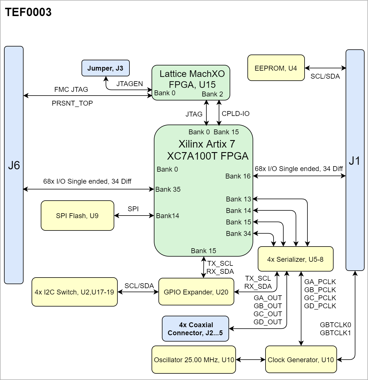 Image Modified Image Modified
|
|
Main Components
| Page properties |
|---|
|
Notes : - Picture of the PCB (top and bottom side) with labels of important components
- Add List below
|
...
| Scroll Title |
|---|
| anchor | Figure_OV_MC |
|---|
| title | TEF0003 main components |
|---|
|
| Scroll Ignore |
|---|
| draw.io Diagram |
|---|
| border | false |
|---|
| viewerToolbar | true |
|---|
| |
|---|
| fitWindow | false |
|---|
| diagramDisplayName | |
|---|
| lbox | true |
|---|
| revision | 7 |
|---|
| diagramName | TEF0003_OV_MC |
|---|
| simpleViewer | false |
|---|
| width | |
|---|
| links | auto |
|---|
| tbstyle | hidden |
|---|
| diagramWidth | 641 |
|---|
|
|
| Scroll Only |
|---|
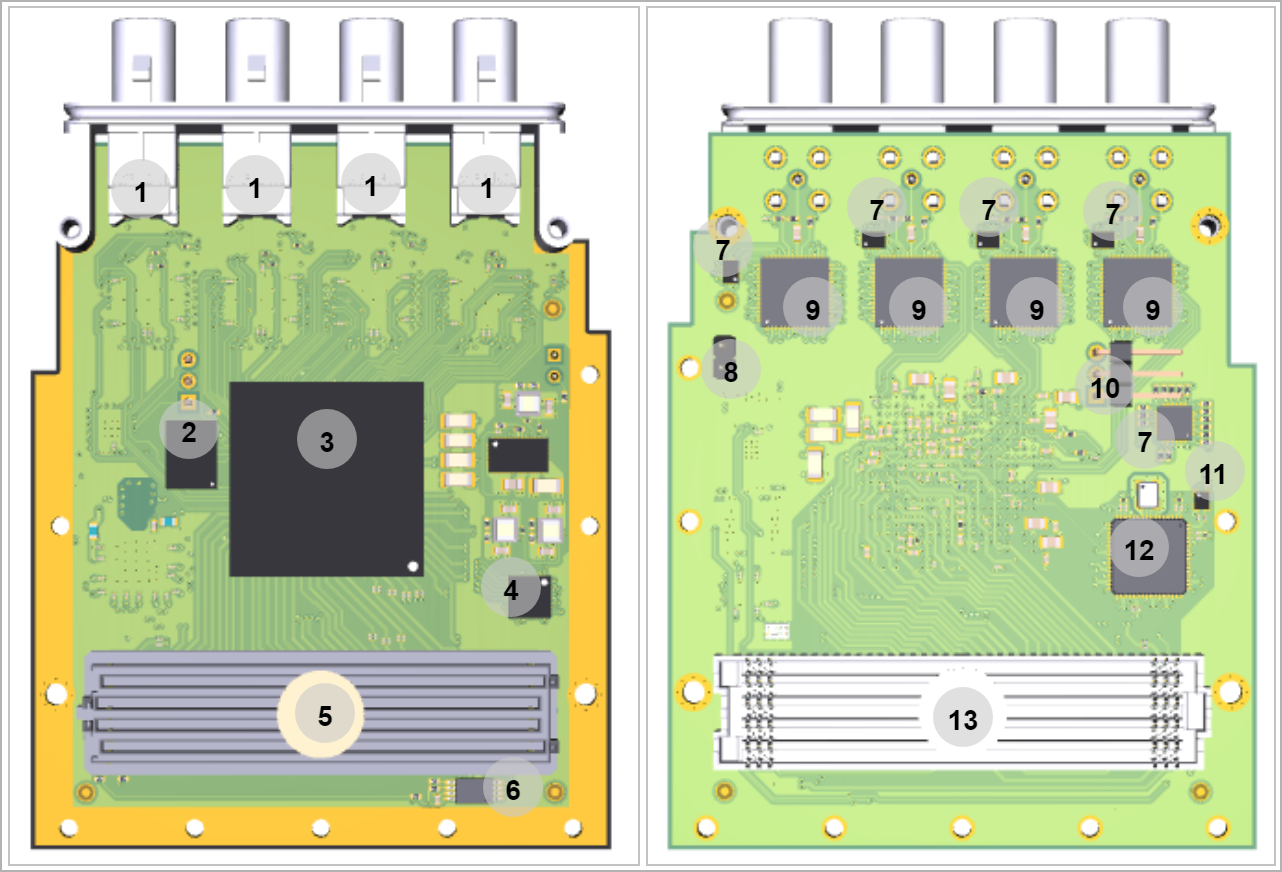 Image Modified Image Modified
|
|
- Coaxial Connectors, J2-5
- SPI Flash, U9
- Xilinx Artix 7 FPGA, U1
- Lattice MachXO FPGA, U15
- Vita 57 ConnectorFMC Adapter, J1
- EEPROM, U4
- I2C Switches, U2, U17-20
- Jumper, J7
- Serializer, U5-8
- Connector Header, J8
- Oscillator 25MHz, U11
- Programmable Clock Generator, U10
- Vita 57 ConnectorFMC Adapter, J6
Initial Delivery State
| Page properties |
|---|
|
Notes : Only components like EEPROM, QSPI flash and DDR3 can be initialized by default at manufacture. If there is no components which might have initial data ( possible on carrier) you must keep the table empty |
...
| Scroll Title |
|---|
| anchor | Table_OV_IDS |
|---|
| title | Initial delivery state of programmable devices on the module |
|---|
|
| Scroll Table Layout |
|---|
| orientation | portrait |
|---|
| sortDirection | ASC |
|---|
| repeatTableHeaders | default |
|---|
| sortByColumn | 1 |
|---|
| sortEnabled | false |
|---|
| cellHighlighting | true |
|---|
|
Storage device name | Content | Notes |
|---|
SPI Flash | Not programmed |
| | EEPROM | Not Programmed |
| | Clock Generator | Programmed |
|
|
Configuration Signals
| Page properties |
|---|
|
- Overview of Boot Mode, Reset, Enables.
|
...
| Scroll Title |
|---|
| anchor | Table_OV_RST |
|---|
| title | Reset processProcess. |
|---|
|
| Scroll Table Layout |
|---|
| orientation | portrait |
|---|
| sortDirection | ASC |
|---|
| repeatTableHeaders | default |
|---|
| sortByColumn | 1 |
|---|
| sortEnabled | false |
|---|
| cellHighlighting | true |
|---|
|
| B2B | I/O | Note | MUX_RESET | - | -| Description | Note |
|---|
PRSNT_TOP | Lattice MachXO Configuration Pin |
| | PROG_B | Artix 7 Configuration Pin | Pulled up to 1.8 |
|
Signals, Interfaces and Pins
| Page properties |
|---|
|
Notes : - For carrier or stand-alone boards use subsection for every connector type (add designator on description, not on the subsection title), for example:
- For modules which needs carrier use only classes and refer to B2B connector if more than one is used, for example
|
...
FMC Connectors
FPGA bank number and number of I/O signals connected to the B2B connector:FMC Connectors J1 and J6 which are located on top and bottom of the board.
| Scroll Title |
|---|
| anchor | Table_SIP_B2BFMC |
|---|
| title | General PL I/O to B2B connectors FMC Connectors information |
|---|
|
| Scroll Table Layout |
|---|
| orientation | portrait |
|---|
| sortDirection | ASC |
|---|
| repeatTableHeaders | default |
|---|
| sortByColumn | 1 |
|---|
| sortEnabled | false |
|---|
| cellHighlighting | true |
|---|
|
| FPGA | FPGA Bank | Connector Designator | I/O Signal Count | Voltage Level | Notes |
|---|
| Artix 7, U1 | 16 | J1B | 68 Single Ended, 34 Differential | 1.8V |
| | 35 | J6B | 68 Single Ended, |
34| 34 Differential | 1.8V |
| | Lattice MachXO, U | 0 | J1F | 4 Single Ended | 3.3V | CPLD | | 0 | J6F | 4 Single Ended | 3.3V |
|
...
Coaxial Connectors
| Scroll Title |
|---|
| anchor | Table_SIP_JTGCoaxial |
|---|
| title | JTAG pins connectionCoaxial Connectors information |
|---|
|
| Scroll Table Layout |
|---|
| orientation | portrait |
|---|
| sortDirection | ASC |
|---|
| repeatTableHeaders | default |
|---|
| sortByColumn | 1 |
|---|
| sortEnabled | false |
|---|
| cellHighlighting | true |
|---|
|
JTAG Signal | B2B Connector |
|---|
| FMC_TMS | J6F-TCK | | FMC_TDI_TOP | J6F-J1-TDI | | FMC_TDO_TOP | J6F-TDO | | FMC_TCK | J6F-TCK | | JTAGEN | J7 | |
MIO Pins
| Schematic | Connected to | Notes |
|---|
| J2 | GA_OUT | Serializer, U5 |
| | J3 | GB_OUT | Serializer, U6 |
| | J4 | GC_OUT | Serializer, U7 |
| | J5 | GD_OUT | Serializer, U8 |
|
|
JTAG Interface
The Lattice MachXO (U15) is available to meet the requirement of a CPLD, JTAG access to the MachXO is available through FMC Adapter J6. JTAG access to the Artix 7(U1) is available via MachXO, Bank 2.
| Scroll Title |
|---|
| anchor | Table_SIP_CPLDJTG |
|---|
| title | CPLD JTAG pins connection |
|---|
|
| Scroll Table Layout |
|---|
| orientation | portrait |
|---|
| sortDirection | ASC |
|---|
| repeatTableHeaders | default |
|---|
| sortByColumn | 1 |
|---|
| sortEnabled | false |
|---|
| cellHighlighting | true |
|---|
|
JTAG Signal | B2B Connector | Notes |
|---|
| FMC_TMS | J6F-TCK |
| | FMC_TDI_TOP | J6F-J1-TDI |
| | FMC_TDO_TOP | J6F-TDO |
| | FMC_TCK | J6F-TCK |
| | JTAGEN | Pulled down |
|
|
| Scroll Title |
|---|
| anchor | Table_SIP_JTG |
|---|
| title | JTAG pins connection |
|---|
|
| Scroll Table Layout |
|---|
| orientation | portrait |
|---|
| sortDirection | ASC |
|---|
| repeatTableHeaders | default |
|---|
| sortByColumn | 1 |
|---|
| sortEnabled | false |
|---|
| cellHighlighting | true |
|---|
|
JTAG Signal | Connected to | Note |
|---|
| TMS | Lattice MachXO, U15 BankArtix 7 FPGA, U1 | Bank 2 Bank 0 | | TDI | Lattice MachXO, U15 Artix 7 FPGA, U1 | Bank 2 Bank 0 | | TDO | Lattice MachXO, U15 Artix 7 FPGA, U1 | Bank 2 Bank 0 | | TCK | Lattice MachXO, U15 Artix 7 FPGA, U1 | Bank 2 Bank 0 | | INIT | Artix 7 FPGA, U1 | Pulled up to 1.8 |
|
| Page properties |
|---|
|
you must fill the table below with group of MIOs which are connected to a specific components or peripherals, you do not have to specify pins in B2B, Just mention which B2B is connected to MIOs. The rest is clear in the Schematic.
Example:
| MIO Pin | Connected to | B2B | Notes |
|---|
| MIO12...14 | SPI_CS , SPI_DQ0... SPI_DQ3 SPI_SCK | J2 | QSPI |
| Scroll Title |
|---|
| anchor | Table_OBP_MIOs |
|---|
| title | MIOs pins |
|---|
|
| Scroll Table Layout |
|---|
| orientation | portrait |
|---|
| sortDirection | ASC |
|---|
| repeatTableHeaders | default |
|---|
| sortByColumn | 1 |
|---|
| sortEnabled | false |
|---|
| cellHighlighting | true |
|---|
|
| MIO Pin | Connected to | B2B | Notes
|
On-board Peripherals
| Page properties |
|---|
|
Notes : - add subsection for every component which is important for design, for example:
- Two 100 Mbit Ethernet Transciever PHY
- USB PHY
- Programmable Clock Generator
- Oscillators
- eMMCs
- RTC
- FTDI
- ...
- DIP-Switches
- Buttons
- LEDs
|
...
| Scroll Title |
|---|
| anchor | Table_OBP |
|---|
| title | On board peripherals |
|---|
|
| Scroll Table Layout |
|---|
| orientation | portrait |
|---|
| sortDirection | ASC |
|---|
| repeatTableHeaders | default |
|---|
| sortByColumn | 1 |
|---|
| sortEnabled | false |
|---|
| cellHighlighting | true |
|---|
|
|
Quad SPI Flash Memory
| Page properties |
|---|
|
Notes : Minimum and Maximum density of quad SPI flash must be mentioned for other assembly options. |
TEF0003 is equipped with a 512Mb Serial NOR Flash (x1/x2/x4) which is provided to store an application on in the SPI Flash memory in order to boot the module. The SPI Flash data is connected to Artix 7 FPGBA via FPGA Bank 14.
| Scroll Title |
|---|
| anchor | Table_OBP_SPI |
|---|
| title | Quad SPI interface MIOs and pins |
|---|
|
| Scroll Table Layout |
|---|
| orientation | portrait |
|---|
| sortDirection | ASC |
|---|
| repeatTableHeaders | default |
|---|
| sortByColumn | 1 |
|---|
| sortEnabled | false |
|---|
| cellHighlighting | true |
|---|
|
| Schematic | U11 U9 Pin | Notes |
|---|
| SPI-CS | CS |
| | SPI-CLK | CLK |
| | SPI-DQO | DI/IO0 |
| | SPI_DQ3 | HOLD/IO3 |
| | SPI-DQ2 | WP/IO2 |
| | SPI-DQ1 | DO/IO1 |
| | 1.8V | VCC |
|
|
EEPROM
A
...
microchip serial EEPROM (U4) is provided for IPMI data. It is accessible via the LPC FMC connector J1 (SCL, SDA).
| Scroll Title |
|---|
| anchor | Table_OBP_EEP |
|---|
| title | I2C EEPROM interface MIOs and pins |
|---|
|
| Scroll Table Layout |
|---|
| orientation | portrait |
|---|
| sortDirection | ASC |
|---|
| repeatTableHeaders | default |
|---|
| sortByColumn | 1 |
|---|
| sortEnabled | false |
|---|
| cellHighlighting | true |
|---|
|
Vita 57 ConnectorU4 PinNotesSCLSDAA0 |
| | A2 | - | - | Pulled Low | | WP | - | - | Pulled Low |
A1
|
| Scroll Title |
|---|
| anchor | Table_OBP_I2C_EEPROM |
|---|
| title | I2C address for EEPROM |
|---|
|
| Scroll Table Layout |
|---|
| orientation | portrait |
|---|
| sortDirection | ASC |
|---|
| repeatTableHeaders | default |
|---|
| sortByColumn | 1 |
|---|
| sortEnabled | false |
|---|
| cellHighlighting | true |
|---|
|
| I2C Address | Designator | Notes |
|---|
0x50 | | 0xA0 | U4 | Write operations are enabled |
U4
|
Clock Sources
| Scroll Title |
|---|
| anchor | Table_OBP_CLK |
|---|
| title | Osillators |
|---|
|
| Scroll Table Layout |
|---|
| orientation | portrait |
|---|
| sortDirection | ASC |
|---|
| repeatTableHeaders | default |
|---|
| sortByColumn | 1 |
|---|
| sortEnabled | false |
|---|
| cellHighlighting | true |
|---|
|
| Designator | Description | Frequency | Note |
|---|
| U4U11 | Oscillator, | 25 MHz.00 MHz | MHz |
| | U10 | Programmable Clock Generator | MHzVariable |
|
|
Programmable Clock Generator
There is a Silicon Labs I2C programmable clock generator on-board (U10) in order to generate reference clocks for the module. Programming can be done using I2C via PIN header J8. done using I2C via PIN header J8. The I2C Address is 0x69.
| Scroll Title |
|---|
| anchor | Table_OBP_PCLK |
|---|
| title | Programmable Clock Generator Inputs and Outputs |
|---|
|
| Scroll Table Layout |
|---|
| orientation | portrait |
|---|
| sortDirection | ASC |
|---|
| repeatTableHeaders | default |
|---|
| sortByColumn | 1 |
|---|
| sortEnabled | false |
|---|
| cellHighlighting | true |
|---|
|
Si5345A Pin
| Signal Name / Description
| Connected To | Direction | Note |
|---|
IN0 | Reference input clock. | U11 | Input | 25.00 MHz oscillator, SiT8008BI | | IN1 |
|
...
A1
...
-
...
| FMCT_GBTCLK0 | J6E | Input | FMC Pcam Adapter | | IN2 | FMCT_GBTCLK1 | J6E | Input | FMC Pcam Adapter | | IN3 | FMCT_CLK0 | J6E | Input | FMC Pcam Adapter | XAXB | - | GND |
|
...
...
...
...
...
CLKPLL2F
...
FPGA bank 2.
...
-
...
Not connected.
...
Output
...
| PLL_SCL | J8, U20 | Input | EEPROM | | SDA | PLL_SDA | J8, U20 | Input | EEPROM | | OUT0 | GA_PCLK | U5/U1 | Output | FPGA bank 15 | | OUT1 | GB_PCLK | U6/U1 | Output | FPGA bank 15 | | OUT2 | GC_PCLK | U7/U1 | Output | FPGA bank 15 | | OUT3 | GD_PCLK | U8/U1 | Output | FPGA bank 15 | | OUT4 | CLK4_P | U1H | Output |
| | OUT5 | GBTCLK0 | J1E/J6E | Output |
| | OUT6 | GBTCLK1 | J1E/J6E | Output |
| | OUT7 | GBTCLK0 | J1E | Output |
| | OUT8/OUT9 | CLK8/CLK9 | Pulled low | Output |
|
|
Power and Power-On Sequence
| Page properties |
|---|
|
In 'Power and Power-on Sequence' section there are three important digrams which must be drawn: - Power on-sequence
- Power distribution
- Voltage monitoring circuit
|
Power Supply
Power supply with minimum current capability of 3 A for system startup is recommended.
Power Consumption
| Scroll Title |
|---|
| anchor | Table_PWR_PC |
|---|
| title | Power Consumption |
|---|
|
| Scroll Table Layout |
|---|
| orientation | portrait |
|---|
| sortDirection | ASC |
|---|
| repeatTableHeaders | default |
|---|
| sortByColumn | 1 |
|---|
| sortEnabled | false |
|---|
| cellHighlighting | true |
|---|
|
| Power Input Pin | Typical Current |
|---|
| VIN3P3V | TBD* |
|
* TBD - To Be Determined
Power Distribution Dependencies
| Scroll Title |
|---|
| anchor | Figure_PWR_PD |
|---|
| title | Power Distribution |
|---|
|
| Scroll Ignore |
|---|
| draw.io Diagram |
|---|
| border | truefalse |
|---|
| viewerToolbar | true |
|---|
| |
|---|
| fitWindow | false |
|---|
| diagramDisplayName | |
|---|
| lbox | true |
|---|
| revision | 7 |
|---|
| diagramName | TEF0003_PWR_PD |
|---|
| simpleViewer | false |
|---|
| | simpleViewer | false |
|---|
| width | |
|---|
| links | auto |
|---|
| tbstyle | hidden | width |
|---|
| diagramWidth | 641 | revision | 1 |
|---|
|
|
| Scroll Only |
|---|
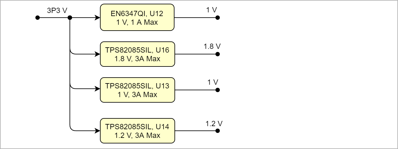 Image Modified Image Modified
|
|
Power-On Sequence
| Scroll Title |
|---|
| anchor | Figure_PWR_PS |
|---|
| title | Power Sequency |
|---|
|
| Scroll Ignore |
|---|
Create DrawIO object here: Attention if you copy from other page, objects are only linked. |
| Scroll Only |
|---|
image link to the generate DrawIO PNG file of this page. This is a workaround until scroll pdf export bug is fixed |
|
Voltage Monitor Circuit
| draw.io Diagram |
|---|
| border | false |
|---|
| viewerToolbar | true |
|---|
| |
|---|
| fitWindow | false |
|---|
| diagramDisplayName | |
|---|
| lbox | true |
|---|
| revision | 2 |
|---|
| diagramName | TEF0003_PWR_PS |
|---|
| simpleViewer | false |
|---|
| width | |
|---|
| links | auto |
|---|
| tbstyle | hidden |
|---|
| diagramWidth | 641 |
|---|
|
|
| Scroll Only |
|---|
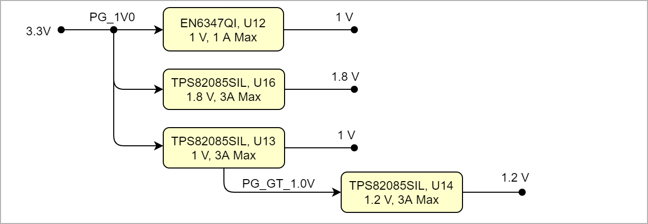 Image Added Image Added
|
|
| Scroll Title |
|---|
| anchor | Figure_PWR_VMC |
|---|
| title | Voltage Monitor Circuit |
|---|
|
| Scroll Ignore |
|---|
Create DrawIO object here: Attention if you copy from other page, objects are only linked. |
| Scroll Only |
|---|
image link to the generate DrawIO PNG file of this page. This is a workaround until scroll pdf export bug is fixed |
|
Power Rails
| Scroll Title |
|---|
| anchor | Table_PWR_PR |
|---|
| title | Module power rails. |
|---|
|
| Scroll Table Layout |
|---|
| orientation | portrait |
|---|
| sortDirection | ASC |
|---|
| repeatTableHeaders | default |
|---|
| sortByColumn | 1 |
|---|
| sortEnabled | false |
|---|
| cellHighlighting | true |
|---|
| | sortEnabled | false |
|---|
| cellHighlighting | true |
|---|
|
| Power Rail Name | FMC Adapter J1G Pin | FMC Adapter J6G Pin | Direction | Notes |
|---|
| 12V | C35, C37 | C35, C37 | Input |
| | 3P3VAUX | D32 | D32 | Input |
| | 3P3V | D36, D38, D40, C39 | D36, D38, D40, C39 | Input |
| VREFA | H1 | H1 | Input |
| | VREFB | K1 | K1 | Input |
| | VIOB | J39, K40 | J39, K40 | Input |
| | VADJ | H40, G39, F40, E39 | H40, G39, F40, E39 | Input |
Power Rail Name | B2B Connector JM1 Pin | B2B Connector JM2 Pin | B2B Connector JM3 Pin | Direction | Notes
|
Bank Voltages
| Scroll Title |
|---|
| anchor | Table_PWR_BV |
|---|
| title | Zynq SoC bank voltages. |
|---|
|
| Scroll Table Layout |
|---|
| orientation | portrait |
|---|
| sortDirection | ASC |
|---|
| repeatTableHeaders | default |
|---|
| sortByColumn | 1 |
|---|
| sortEnabled | false |
|---|
| cellHighlighting | true |
|---|
|
| Schematic Name | | Notes |
|---|
|
...
| default |
|---|
| sortByColumn | 1 |
|---|
| sortEnabled | false |
|---|
| cellHighlighting | true |
|---|
|
| Schematic Name | | Notes |
|---|
| Bank 13 | VCCO_13 | 1.8 V |
| | Bank 14 | VCCO_14 | 1.8 V |
| | Bank 15 | VCCO_15 | 1.8 V |
| | Bank 16 | VCCO_16 | VADJ | 1.8 V | | Bank 34 | VCCO_34 | 1.8 V |
| | Bank 35 | VCCO_35 | VADJ | 1.8 V | | Bank 0 | VCCO_0 | 1.8 V |
|
| Page properties |
|---|
|
| This section is optional and only for modules. use "include page" macro and link to the general B2B connector page of the module series, For example: 6 x 6 SoM LSHM B2B Connectors
| Include Page |
|---|
| PD:6 x 6 SoM LSHM B2B Connectors | PD:6 x 6 SoM LSHM B2B Connectors
Technical Specifications
Absolute Maximum Ratings
| Scroll Title |
|---|
| anchor | Table_TS_AMR |
|---|
| title | PS absolute maximum ratings |
|---|
|
| Scroll Table Layout |
|---|
| orientation | portrait |
|---|
| sortDirection | ASC |
|---|
| repeatTableHeaders | default |
|---|
| sortByColumn | 1 |
|---|
| sortEnabled | false |
|---|
| cellHighlighting | true |
|---|
|
| Max | Unit | V | | Max | Unit |
|---|
| 3P3V | Input Supply Voltage | -0.5 | 3.75 |
VV | | T_STG | Storage Temperature | -40 | 85 | °C |
V | V | V | V
|
Recommended Operating Conditions
Operating temperature range depends also on customer design and cooling solution. Please contact us for options.
| Scroll Title |
|---|
| anchor | Table_TS_ROC |
|---|
| title | Recommended operating conditions. |
|---|
|
| Scroll Table Layout |
|---|
| orientation | portrait |
|---|
| sortDirection | ASC |
|---|
| repeatTableHeaders | default |
|---|
| sortByColumn | 1 |
|---|
| sortEnabled | false |
|---|
| cellHighlighting | true |
|---|
|
| Parameter | Min | Max | Units | Reference Document |
|---|
V | See ???? datasheets. | V | See Xilinx ???? datasheet. | V | See Xilinx ???? datasheet. | V | See Xilinx ???? datasheet. | V | See Xilinx ???? datasheet. | V | See Xilinx ???? datasheet. | V | See Xilinx ???? datasheet. | °C | See Xilinx ???? datasheet. | | 3P3V | 2.375 | 3.465 | V |
| | T_OPR | -40 | 85 | °C | See MT25QU512ABB8E12-0SIT (U9) |
°C | See Xilinx ????
|
Physical Dimensions
Module size: 84 mm × 65 mm. Please download the assembly diagram for exact numbers.
Mating height with standard connectors: 10 mm.
PCB thickness: 1.54 56 mm.
| Page properties |
|---|
|
In 'Physical Dimension' section, top and bottom view of module must be inserted, information regarding physical dimensions can be obtained through webpage for product in Shop.Trenz, (Download> Documents> Assembly part) for every SoM. For Example: for Module TE0728, Physical Dimension information can be captured by snipping tools from the link below: https://www.trenz-electronic.de/fileadmin/docs/Trenz_Electronic/Modules_and_Module_Carriers/5.2x7.6/TE0745/REV02/Documents/AD-TE0745-02-30-1I.PDF
|
...
| Scroll Title |
|---|
| anchor | Figure_TS_PD |
|---|
| title | Physical Dimension |
|---|
|
| draw.io Diagram |
|---|
| border | false |
|---|
| viewerToolbar | true |
|---|
| |
|---|
| fitWindow | false |
|---|
| diagramDisplayName | |
|---|
| lbox | true |
|---|
| revision | 25 |
|---|
| diagramName | TEF0003_TS_PD |
|---|
| aspect | 5e705185-5827-752c-089d-756568e6698bTEF0003_TS_PD |
|---|
| simpleViewer | false |
|---|
| width | 639 |
|---|
| aspectHash | 7695f7bc00c98da1082cb1c11a0a6258edf875fc |
|---|
| links | auto |
|---|
| tbstyle | hidden |
|---|
| diagramWidth | 436 |
|---|
|
| Scroll Only |
|---|
| scroll-pdf | true |
|---|
| scroll-office | true |
|---|
| scroll-chm | true |
|---|
| scroll-docbook | true |
|---|
| scroll-eclipsehelp | true |
|---|
| scroll-epub | true |
|---|
| scroll-html | true |
|---|
| 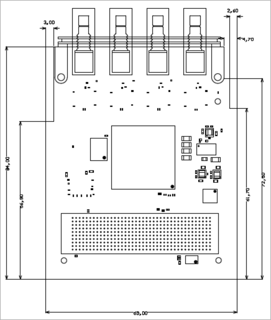 Image Modified Image Modified
|
|
Currently Offered Variants
| Page properties |
|---|
|
Set correct link to the shop page overview table of the product on English and German. Example for TE0728: ENG Page: https://shop.trenz-electronic.de/en/Products/Trenz-Electronic/TE07XX-Zynq-SoC/TE0728-Zynq-SoC/ DEU Page: https://shop.trenz-electronic.de/de/Produkte/Trenz-Electronic/TE07XX-Zynq-SoC/TE0728-Zynq-SoC/ For Baseboards or modules, where no overview page is available (and revision number is coded in the direct link) use shop search link, e.g. TE0706: ENG Page: https://shop.trenz-electronic.de/en/search?sSearch=TE0706 DEU Page: https://shop.trenz-electronic.de/de/search?sSearch=TE0706 |
...
| Scroll Title |
|---|
| anchor | Table_VCP_SO |
|---|
| title | Trenz Electronic Shop Overview |
|---|
|
| Scroll Table Layout |
|---|
| orientation | portrait |
|---|
| sortDirection | ASC |
|---|
| repeatTableHeaders | default |
|---|
| sortByColumn | 1 |
|---|
| sortEnabled | false |
|---|
| cellHighlighting | true |
|---|
|
|
Revision History
Hardware Revision History
...
| Scroll Title |
|---|
| anchor | Table_RH_HRH |
|---|
| title | Hardware Revision History |
|---|
|
| Scroll Table Layout |
|---|
| orientation | portrait |
|---|
| sortDirection | ASC |
|---|
| repeatTableHeaders | default |
|---|
| sortByColumn | 1 |
|---|
| sortEnabled | false |
|---|
| cellHighlighting | true |
|---|
|
| Date | Revision | Changes | Documentation Link |
|---|
| 2017-06-27 | REV01 | Initial Release | REV01 |
|
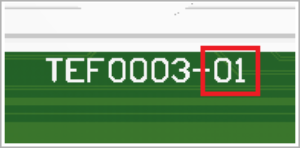
Hardware revision number can be found on the PCB board together with the module model number separated by the dash.
| Scroll Title |
|---|
| anchor | Figure_RV_HRN |
|---|
| title | Board hardware revision number. |
|---|
|
| Scroll Ignore |
|---|
| draw.io Diagram |
|---|
| border | false |
|---|
| viewerToolbar | true |
|---|
| |
|---|
| fitWindow | false |
|---|
| diagramDisplayName | |
|---|
| lbox | true |
|---|
| revision | 14 |
|---|
| diagramName | TEF0003_RV_HRN |
|---|
| simpleViewer | false |
|---|
| width | |
|---|
| links | auto |
|---|
| tbstyle | hidden |
|---|
| diagramWidth | 290196 |
|---|
|
|
| Scroll Only |
|---|
|
|
Document Change History
| Page properties |
|---|
|
- Note this list must be only updated, if the document is online on public doc!
- It's semi automatically, so do following
Add new row below first Copy "Page Information Macro(date)" Macro-Preview, Metadata Version number, Author Name and description to the empty row. Important Revision number must be the same as the Wiki document revision number Update Metadata = "Page Information Macro (current-version)" Preview+1 and add Author and change description. --> this point is will be deleted on newer pdf export template - Metadata is only used of compatibility of older exports
|
...
| Scroll Title |
|---|
| anchor | Table_RH_DCH |
|---|
| title | Document change history. |
|---|
|
| Scroll Table Layout |
|---|
| orientation | portrait |
|---|
| sortDirection | ASC |
|---|
| repeatTableHeaders | default |
|---|
| sortByColumn | 1 |
|---|
| sortEnabled | false |
|---|
| cellHighlighting | true |
|---|
|
| Date | Revision | Contributor | Description |
|---|
| Page info |
|---|
| infoType | Modified date |
|---|
| dateFormat | yyyy-MM-dd |
|---|
| type | Flat |
|---|
|
| | Page info |
|---|
| infoType | Current version |
|---|
| prefix | v. |
|---|
| type | Flat |
|---|
| showVersions | false |
|---|
|
| | Page info |
|---|
| infoType | Modified by |
|---|
| type | Flat |
|---|
| showVersions | false |
|---|
|
| | -- | all | | Page info |
|---|
| infoType | Modified users |
|---|
| type | Flat |
|---|
| showVersions | false |
|---|
|
| |
|
Disclaimer
| Include Page |
|---|
| IN:Legal Notices |
|---|
| IN:Legal Notices |
|---|
|
| draw.io Diagram |
|---|
| border | false |
|---|
| viewerToolbar | true |
|---|
| fitWindow | false |
|---|
diagramDisplayName | | lbox | true |
|---|
| revision | 7 |
|---|
| diagramName | TEF0003_OV_MC |
|---|
| simpleViewer | false |
|---|
width | | links | auto |
|---|
| tbstyle | hidden |
|---|
| diagramWidth | 641 |
|---|
|