Page History
...
| HTML |
|---|
<!-- Template Revision 1.3 beta (HTML comment will not display, it's not needed to remove them. For Template/Skeleton changes, increase Template Revision number. So we can check faster, if the TRM style is up to date) --> |
| Scroll Ignore |
|---|
| Scroll pdf ignore | |
|---|---|
Table of Contents
|
Overview
| Scroll Only (inline) |
|---|
Refer to "https://shop.trenz-electronic.de/en/Download/?path=Trenz_Electronic/TE0808" for downloadable version of this manual and the rest of available documentation. |
The Trenz Electronic TE0808 is an industrial-grade MPSoC SoM integrating a Xilinx Zynq UltraScale+ MPSoC, max. 8 GByte up to 8 GBytes of DDR4 SDRAM with via 64-Bit width databus connectionbit wide data bus, max. 512 MByte Flash memory for configuration and operation, 20 Gigabit transceivers and powerful switch-mode power supplies for all on-board voltages. A large number of configurable I/O's is Os are provided via rugged high-speed stacking connections. All this in a compact 5.2 x 7.6 cm form factor, at the most competitive price.
| Scroll Only (inline) |
|---|
Refer to http://trenz.org/te0808-info for the current online version of this manual and other available documentation.
|
| Note |
| Important Information for TE0808 boards which are equipped with ES1 or ES2 silicon: Erratas and functional restrictions may exist, please check Xilinx documentation and contact your local Xilinx FAE for restrictions. |
Key Features
- MPSoC: ZYNQ UltraScale+ ZU9EG 900 pin package
- Memory
- 64-Bit DDR4, 8 GByte maximum
- Dual SPI boot Flash in parallel, 512 MByte maximum - User I/OOs
- 65 x MIOPS MIOs, 48 x PL HD (all)GPIOs, 156 x PL HP GPIOs (3 banks)
- Serial transceivertransceivers: 4 x GTR + 16 x GTH
- Transceiver clocks inputs and outputs
- PLL clock generator inputs and outputs - Size: 52 x 76 mm, 3 mm mounting holes for skyline heat spreader
- B2B connectors: 4 x 160 pin
- Si5345 - 10 Si5345 - 10 output PLL
- All power supplies on board, single 3.3V power source required
- 14 on-board DC-DC regulators and 13 LDOs
- LP, FP, PL separately controlled power domains - Support for all boot modes (except NAND) and scenarios
- Support for any combination of PS connected peripherals
- Size: 52 x 76 mm, 3 mm mounting holes for skyline heat spreader
- B2B connectors: 4 x 160 pin
Block Diagram
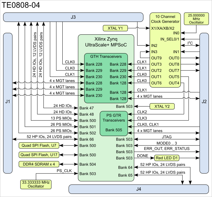
Figure 1: TE0808-04 Block Diagram.
...
- Xilinx ZYNQ UltraScale+ XCZU9EG MPSoC, U1
- Low-power programmable oscillator @ 33.333333 MHz (PS_CLK), U32
- Red LED (DONE), D1
- 256Mx16 DDR4-2400 SDRAM, U12
- 256Mx16 DDR4-2400 SDRAM, U9
- 256Mx16 DDR4-2400 SDRAM, U2
- 256Mx16 DDR4-2400 SDRAM, U3
- 12A PowerSoC DCDC DC-DC converter, U4
- Quartz crystal, Y1
- Low-power programmable oscillator @ 25.000000 MHz (IN0 for U5), U25
- 10-channel programmable PLL clock generator, U5
- Ultra fine 0.50 mm pitch, Razor Beam™ LP Slim Terminal Strip with 160 contacts, J4
- Ultra fine 0.50 mm pitch, Razor Beam™ LP Slim Terminal Strip with 160 contacts, J2
- Ultra fine 0.50 mm pitch, Razor Beam™ LP Slim Terminal Strip with 160 contacts, J3
- Ultra fine 0.50 mm pitch, Razor Beam™ LP Slim Terminal Strip with 160 contacts, J1
- Quartz crystal, Y2
- 256 Mbit serial NOR Flash memory, U7
- 256 Mbit serial NOR Flash memory, U17
...
Each connector has a specific arrangement of the signal pins, which are grouped together in categories related to their functionalities and to their belonging to particular units of the Zynq UltrascaleUltraScale+ MPSoC like I/O - banks, interfaces and Gigabit transceivers
or to the on-board peripherals.
...
| Bank | Type | B2B Connector | Schematic Names / Connector Pins | I/O Signal CountSignals | LVDS Pairs Count | VCCO Bank Voltage | Notes |
|---|---|---|---|---|---|---|---|
| 47 | HD | J3 | B47_L1_P ... B47_L12_P | 24 I/O'sOs | 12 | VCCO47 | VCCO max. 3.3V |
| 48 | HD | J3 | B48_L1_P ... B48_L12_P | 24 I/O'sOs | 12 | VCCO48 | VCCO max. 3.3V |
| 64 | HP | J4 | B64_L1_P ... B64_L24_P B_64_T0 ... B_64_T3 | 52 I/O's | 24 | VCCO64 | VCCO max. 1.8V |
| 65 | HP | J4 | B65_L1_P ... B65_L24_P B_65_T0 ... B_65_T3 | 52 I/O'sOs | 24 | VCCO65 | VCCO max. 1.8V |
| 66 | HP | J1 | B66_L1_P ... B66_L24_P B_66_T0 ... B_66_T3 | 48 I/O'sOs | 24 | VCCO66 | VCCO max. 1.8V |
| 500 | MIO | J3 | MIO13 ... MIO25 | 13 I/O'sOs | - | PS_1V8 | user User configurable I/O's Os on B2B |
| 501 | MIO | J3 | MIO26 ... MIO51 | 26 I/O'sOs | - | PS_1V8 | user User configurable I/O's Os on B2B |
| 502 | MIO | J3 | MIO52 ... MIO77 | 26 I/O'sOs | - | PS_1V8 | user User configurable I/O's Os on B2B |
Table 2: B2B connector pin-outs of available PL and PS banks of the TE0808-04 SoM.
All MIO banks are powered from on-module DC-DC power rail. All PL I/O Banks have separate VCCO pins in the B2B connectors, valid VCCO should be supplied from the baseboard.
...
| Bank | Type | B2B Connector | Count of MGT Lanes | Schematic Names / Connector Pins | MGT Bank's Reference Clock Inputs |
|---|---|---|---|---|---|
| 228 | GTH | J1 | 4 GTH lanes (4 RX / 4 TX) | B228_RX3_P, B228_RX3_N, pins J1-2751, J1-2953 B228_RX2_P, B228_RX2_N, pins J1-3357, J1-3559 B228_RX1_P, B228_RX1_N, pins J1-3963, J1-4165 B228_RX0_P, B228_RX0_N, pins J1-4569, J1-4771 | 1 reference clock signal (B228_CLK0) from B2B connector 1 reference clock signal (B228_CLK1) from programmable |
| 229 | GTH | J1 | 4 GTH lanes (4 RX / 4 TX) | B229_RX3_P, B229_RX3_N, pins J1-27, J1-29 B229_RX2_P, B229_RX2_N, pins J1-33, J1-35 B229_RX1_P, B229_RX1_N, pins J1-39, J1-41 B229_RX0_P, B229_RX0_N, pins J1-45, J1-47 | 1 reference clock signal (B229_CLK0) from B2B connector 1 reference clock signal (B229_CLK1) from programmable |
| 230 | GTH | J1 | 4 GTH lanes (4 RX / 4 TX) | B230_RX3_P, B230_RX3_N, pins J1-3, J1-5 B230_RX2_P, B230_RX2_N, pins J1-9, J1-11 B230_RX1_P, B230_RX1_N, pins J1-15, J1-17 B230_RX0_P, B230_RX0_N, pins J1-21, J1-23 | 1 reference clock signal (B230_CLK1) from B2B connector 1 reference clock signal (B230_CLK0) from programmable |
| 128 | GTH | J2 | 4 GTH lanes (4 RX / 4 TX) | B128_RX3_N, B128_RX3_P, pins J2-28, J2-30 B128_RX2_N, B128_RX2_P, pins J2-34, J2-36 B128_RX1_N, B128_RX1_P, pins J2-40, J2-42 B128_RX0_N, B128_RX0_P, pins J2-46, J2-48 | 1 reference clock signal (B128_CLK1) from B2B connector 1 reference clock signal (B128_CLK0) from programmable |
| 505 | GTR | J2 | 4 GTR lanes (4 RX / 4 TX) | B505_RX3_N, B505_RX3_P, pins J2-52, J2-54 B505_RX2_N, B505_RX2_P, pins J2-58, J2-60 B505_RX1_N, B505_RX1_P, pins J2-64, J2-66 B505_RX0_N, B505_RX0_P, pins J2-70, J2-72 | 2 reference clock signals (B505_CLK0, B505_CLK1) from B2B connector 2 reference clock signal (B505_CLK2, B505_CLK3) from programmable |
...
JTAG access is provided through the MPSoC's PS configuration bank 503 with bank voltage ' PS_1V8'.
| JTAG Signal | B2B Connector Pin |
|---|---|
| TCK | J2-120 |
| TDI | J2-122 |
| TDO | J2-124 |
| TMS | J2-126 |
...
The Xilinx Zynq UltraScale+ MPSoC's PS configuration bank 503 control signal pins are accessible through B2B - connector J2.
For further information about the particular control signals and how to use and evaluate them, refer to the Xilinx Zynq UltraScale+ MPSoC TRM and UltraScale Architecture Configuration - User Guide.
| Signal | B2B Connector Pin | Function |
|---|---|---|
| DONE | J2-116 | PL configuration completed. |
| PROG_B | J2-100 | PL configuration reset signal. |
| INIT_B | J2-98 | PS is initialized after a power-on reset. |
| SRST_B | J2-96 | System reset. |
| MODE0 ... MODE3 | J2-109/J2-107/J2-105/J2-103 | 4-bit boot mode pins. For further information about the boot - modes refer to the Xilinx Zynq UltraScale+ MPSoC TRM |
| ERR_STATUS / ERR_OUT | J2-86 / J2-88 | ERR_OUT signal is asserted for accidental loss of power, an error, or an exception in the MPSoC's Platform Management Unit (PMU)-. ERR_STATUS indicates a secure lock-down state. |
| PUDC_B | J2-127 | Pull-up during configuration (pulled-up to PL_1V8). |
...
Quad SPI Flash memory ICs U7 and U17 are connected to the Zynq MPSoC PS QSPI0 interface via PS MIO bank 500, pins MIO0 ... MIO5 and MIO7 ... MIO12.
| MIO | Signal Schematic Name | U7 Pin | MIO | Signal Schematic Name | U17 Pin | ||
|---|---|---|---|---|---|---|---|
| 0 | SPI Flash -SCK/M4CLK | B2 | 7 | SPI Flash -SCKCS | C2 | ||
| 1 | SPI Flash -DQ1/M1IO1 | D2 | 8 | SPI Flash -DQ0/M0IO0 | D3 | ||
| 2 | SPI Flash -DQ2/M2IO2 | C4 | 9 | SPI Flash -DQ1/M1IO1 | D2 | ||
| 3 | SPI Flash -DQ3/M3IO3 | D4 | 10 | SPI Flash -DQ2/M2IO2 | C4 | ||
| 4 | SPI Flash -DQ0/M0IO0 | D3 | 11 | SPI Flash -DQ3/M3IO3 | D4 | ||
| 5 | SPI Flash -SCKCS | C2 | 12 | SPI Flash -SCK/M4CLK | B2 |
Table 7: PS MIO pin assignment of the Quad SPI Flash memory ICs.
Boot Process
The boot source device and mode of the Zynq UltraScale+ MPSoC can be selected via 4 dedicated pins, which generate a 4-bit code to select the boot mode. The pins are accessible on B2B connector J2:
...
Table 8: Boot mode pins on B2B connector J2.
Following boot modes are possible on the TE0808 UltraScale+ module by generating the corresponding 4-bit code by the pins ' PS_MODE0 ' ... ' PS_MODE3 ' (little-endian alignment):
...
For functional details see ug1085 - Zynq UltraScale+ TRM (Boot Modes Section).
...
The TE0808-04 SoM is equipped with with four DDR4-2400 SDRAM modules chip with up to 8 GByte memory density. The SDRAM modules chips are connected to the Zynq MPSoC's PS DDR controller (bank 504) with a 64-bit data bus.
Refer to the Xilinx Zynq UltraScale+ datasheet DS925 for more information on whether the specific package of the Zynq UltraScale+ MPSoC supports the maximum data transmission rate of 2400 MByte/s.
Programmable PLL Clock Generator
...
| Input | Connected to | Frequency | Notes |
|---|---|---|---|
| IN0 | On-board Oscillator (U25) | 25.000000 MHz | - |
| IN1 | B2B Connector pins J2-34, J2-1 6 (differential pair) | User | AC decoupling required on base |
| IN2 | B2B Connector pins J3-66, J3-68 (differential pair) | User | AC decoupling required on base |
| IN3 | OUT9 | User | Loop-back from OUT9 |
| Output | Connected to | Frequency | Notes |
| OUT0 | B2B Connector pins J2-3, J2-1 (differential pair) | User | Default off |
| OUT1 | B230 CLK0 | User | Default off |
| OUT2 | B229 CLK1 | User | Default off |
| OUT3 | B228 CLK1 | User | Default off |
| OUT4 | B505 CLK2 | User | Default off |
| OUT5 | B505 CLK3 | User | Default off |
| OUT6 | B128 CLK0 | User | Default off |
| OUT7 | B2B Connector pins J2-713, J2-9 15 (differential pair) | User | Default off |
| OUT8 | B2B Connector pins J2-137, J2-15 9 (differential pair) | User | Default off |
| OUT9 | IN3 (Loop-back) | User | Default off |
| XA/XB | Quartz (Y1) | 50.000 MHz | - |
Table 11: Programmable PLL clock generator input/output.
The Si5345A programmable clock generator's control interface pins are exposed to B2B connector J2. For further information refer to the Si5345A data sheet.
| Signal | B2B Connector Pin | Function |
|---|---|---|
| PLL_FINC | J2-81 | Frequency increment. |
| PLL_LOLN | J2-85 | Loss of lock (active-low). |
| PLL_SEL0 / PLL_SEL1 | J2-93 / J2-87 | Manual input switching. |
| PLL_FDEC | J2-94 | Frequency decrement. |
| PLL_RST | J2-5989 | Device reset (active-low) |
| PLL_SCL / PLL_SDA | J2-90 / J2-92 | I2C interface, external pull-ups needed for SCL / SDA lines. I2C address in current configuration: 1101000b1101001b. |
Table 12: B2B connector pin-out of Si5345A programmable clock generator.
...
Figure 3: Power Distribution Diagram.
| Note |
|---|
Current rating of Samtec Razor Beam™ LSHMBeam LP Terminal/Socket Strip ST5/SS5 B2B connectors is 21.0A 5 A per pin (2 adjacent pins powered1 pin powered per row). |
Power-On Sequence Diagram
...
| Enable-Signal | B2B Connector Pin | Max. Voltage | Note | Power-Good-Signal | B2B Connector Pin | Pull-up Resistor | Note | |||
|---|---|---|---|---|---|---|---|---|---|---|
| EN_LPD | J2-108 | 6V | TPS82085SIL data sheet | LP_GOOD | J2-106 | 4K7, pulled up to LP_DCDC | - | |||
| EN_FPD | J2-102 | DCDCIN | NC7S08P5X data sheet | PG_FPD | J2-110 | 4K7, pulled up to DCDCIN | - | |||
| EN_PL | J2-101 | PL_DCIN | left floating for logic high (drive to GND for logic low) | PG_PL | J2-104 | External pull-up needed (max. voltage GT_DCDC), max. sink current 1 mA | 4K7, pulled up to PL_DCIN | TPS82085SIL /TPS82085SIL / | ||
| EN_DDR | J2-112 | DCDCIN | NC7S08P5X data sheet | PG_DDR | J2-114 | 4K7, pulled up to DCDCIN | - | |||
| EN_PSGT | J2-84 | DCDCIN | NC7S08P5X data sheet | PG_PSGT | J2-82 | External pull-up needed (max. 5.5V), max. sink current 1 mA | TPS74801 data sheet | |||
| EN_GT_R | J2-95 | GT_DCDC | NC7S08P5X data sheet | PG_GT_R | J2-91 | External pull-up needed (max. 5.5V), max. sink current 1 mA | TPS74401 data sheet | |||
| EN_GT_L | J2-79 | GT_DCDC | NC7S08P5X data sheet | PG_GT_L | J2-97 | External pull-up needed (max. 5.5V), max. sink current 1 mA | TPS74801 data sheet | |||
| EN_PLL_PWR | J2-77 | 6V | TPS82085SIL data sheet | PG_PLL_1V8 | J2-80 | External pull-up needed (max. 5.5V), max. sink current 1 mA | TPS82085SIL data sheet |
...
Power Rail Name | B2B J1 Pins | B2B J2 Pins | B2B J3 Pins | Directions | Note |
|---|---|---|---|---|---|
| PL_DCIN | 151, 153, 155, 157, 159 | - | - | Input | - |
| DCDCIN | - | 154, 156, 158, 160, | - | Input | - |
| LP_DCDC | - | 138, 140, 142, 144 | - | Input | - |
| PS_BATT | - | 125 | - | Input | - |
| GT_DCDC | - | - | 157, 158, 159, 160 | Input | - |
| PLL_3V3 | - | - | 152 | Input | U5 (programmable PLL) 3.3V nominal input |
| SI_PLL_1V8 | - | - | 151 | Output | Internal voltage level 1.8V nominal output |
| PS_1V8 | - | 99 | 147, 148 | Output | Internal voltage level |
| PL_1V8 | 91, 121 | - | - | Output | Internal voltage level |
| DDR_1V2 | - | 135 | - | Output | Internal voltage level |
...
B2B connectors
| Include Page | ||||||
|---|---|---|---|---|---|---|
|
Variants Currently In Production
| Module Variant | Zynq UltraScale+ MPSoC | DDR4 | Junction Temperature | Operating Temperature Range | ||
|---|---|---|---|---|---|---|
| TE0808-04-09EG-1EA | XCZU9EG-1FFVC900E | 2GB | 0°C - 100°C | Extended Temperature Range | ||
| TE0808-04-09EG- | 2IB1EB | XCZU9EG- | 2FFVC900I1FFVC900E | 4GB | 0°C - 40°C - 100°C | Industrial Extended Temperature Range |
...
| TE0808-04 |
...
| -09EG-1ED(1) | XCZU9EG-1FFVC900E | 4GB | 0°C - 100°C | Extended Temperature Range |
| TE0808-04-09EG-2IB | XCZU9EG-2FFVC900I | 4GB | -40°C - 100°C | Industrial Temperature Range |
(1) Note: Lower B2B connector profile,check distance bolt of between module and carrier
Table 19: Differences between variants of Module TE0808-04
Technical Specifications
Absolute Maximum Ratings
Technical Specifications
Absolute Maximum Ratings
Parameter | Min | Max | Unit | Notes / Reference Document |
|---|---|---|---|---|
| PL_DCIN | -0.3 | 74 | V | TPS82085SIL / EN63A0QI data sheet / Limit is LP_DCDC over EN/PG |
| DCDCIN | -0.3 | 74 | V | TPS82085SIL / TPS51206 data sheet / Limit is LP_DCDC over EN/PG |
| LP_DCDC | -0.3 | 4 | V | TPS3106K33DBVR data sheet |
| GT_DCDC | -0.3 | 74 | V | TPS82085SIL data sheet / Limit is LP_DCDC over EN/PG |
| PS_BATT | -0.5 | 2 | V | Xilinx DS925 data sheet |
| PLL_3V3 | -0.5 | 3.8 | V | Si5345/44/42 data sheet |
| VCCO for HD I/O banks | -0.5 | 3.4 | V | Xilinx DS925 data sheet |
| VCCO for HP I/O banks | -0.5 | 2 | V | Xilinx DS925 data sheet |
| VREF | -0.5 | 2 | V | Xilinx DS925 data sheet |
| I/O input voltage for HD I/O banks | -0.55 | VCCO + 0.55 | V | Xilinx DS925 data sheet |
| I/O input voltage for HP I/O banks | -0.55 | VCCO + 0.55 | V | Xilinx DS925 data sheet |
| PS I/O input voltage (MIO pins) | -0.5 | VCCO_PSIO + 0.55 | V | Xilinx DS925 data sheet, VCCO_PSIO 1.8V nominally |
Receiver (RXP/RXN) and transmitter | -0.5 | 1.2 | V | Xilinx DS925 data sheet |
Voltage on input pins of | -0.5 | VCC + 0.5 | V | NC7S08P5X data sheet, see schematic for VCC |
Voltage on input pins (nMR) of | -0.3 | VDD + 0.3 | V | TPS3106 data sheet, |
| "Enable"-signals on TPS82085SIL (EN_PLL_PWR, EN_LPD) | -0.3 | 7 | V | TPS82085SIL data sheet |
Storage temperature (ambient) | -40 | 100 | °C | ROHM Semiconductor SML-P11 Series data sheet |
...
| Parameter | Min | Max | Unit | Notes / Reference Document |
|---|---|---|---|---|
| PL_DCIN | 23.53 | 3.6 | V | EN63A0QI / TPS82085SIL data sheet / Limit is LP_DCDC over EN/PG |
| DCDCIN | 3.13 | 3.6 | V | TPS82085SIL / TPS51206PSQ data sheet / Limit is LP_DCDC over EN/PG |
| LP_DCDC | 23.53 | 3.6 | V | TPS82085SIL / TPS3106 TPS3106K33DBVR data sheet |
| GT_DCDC | 23.53 | 3.6 | V | TPS82085SIL data sheet/ Limit is LP_DCDC over EN/PG |
| PS_BATT | 1.2 | 1.5 | V | Xilinx DS925 data sheet |
| PLL_3V3 | 3.14 | 3.47 | V | Si5345/44/42 data sheet 3.3V typical |
| VCCO for HD I/O banks | 1.14 | 3.4 | V | Xilinx DS925 data sheet |
| VCCO for HP I/O banks | 0.95 | 1.9 | V | Xilinx DS925 data sheet |
| I/O input voltage for HD I/O banks. | -0.2 | VCCO + 0.2 | V | Xilinx DS925 data sheet |
| I/O input voltage for HP I/O banks | -0.2 | VCCO + 0.2 | V | Xilinx DS925 data sheet |
| PS I/O input voltage (MIO pins) | -0.2 | VCCO_PSIO + 0.2 | V | Xilinx DS925 data sheet, VCCO_PSIO 1.8V nominally |
| Voltage on input pins of NC7S08P5X 2-Input AND Gate | 0 | VCC | V | NC7S08P5X data sheet, |
Voltage on input pin 'MR' of | 0 | VDD | V | TPS3106 data sheet, |
...
Module size: 52 mm × 76 mm. Please download the assembly diagram for exact numbers
Mating height with standard connectors: 4mm5mm
PCB thickness: 1.6mm
Highest part on PCB: approx. 3mm. Please download the step model for exact numbers
...
| Date | Revision | Notes | Link to PCN | Documentation Link |
|---|---|---|---|---|
| - | 04 | First production silicon | - | TE0808-04 |
| - | 03 | Second ES production release | - | TE0808-03 |
| 2016-03-09 | 02 | First ES production release | - | TE0808-02 |
| - | 01 | Prototypes | - | - |
Hardware revision number is written on the PCB board together with the module model number separated by the dash.

Document Change History
the dash.
Document Change History
| Date | Revision | Contributors | Description | ||||||||||||||||||||||||||
|---|---|---|---|---|---|---|---|---|---|---|---|---|---|---|---|---|---|---|---|---|---|---|---|---|---|---|---|---|---|
|
|
|
| ||||||||||||||||||||||||||
2022-09-13 | v.41 | Vadim Yunitski |
| ||||||||||||||||||||||||||
| 2021-09-07 | V.39 | John Hartfiel |
| ||||||||||||||||||||||||||
| 2021-05-17 | v.37 | John Hartfiel |
| ||||||||||||||||||||||||||
| 2021-03-11 | v.35 | Antti Lukats |
| ||||||||||||||||||||||||||
2019-01-27 | v.30 | Martin Rohrmüller |
| ||||||||||||||||||||||||||
2018-11-20 | v.29 | John Hartfiel |
| ||||||||||||||||||||||||||
2018-08-27 | v.27 | John Hartfiel |
| ||||||||||||||||||||||||||
2028-06-28 | v.26 | John Hartfiel |
| ||||||||||||||||||||||||||
2017-11-13 | v.24 | Ali Naseri |
| ||||||||||||||||||||||||||
2017-11-13 | John Hartfiel |
| |||||||||||||||||||||||||||
| 2017-10-20 | v.21 | Ali Naseri |
| ||||||||||||||||||||||||||
| 2017-08-28 | v.15 | John Hartfiel |
| ||||||||||||||||||||||||||
| 2017-08-28 | v.14 | ||||||||||||||||||||||||||||
| Date | Revision | Contributors | Description | ||||||||||||||||||||||||||
| Page info | modified-date | modified-date | |||||||||||||||||||||||||||
| dateFormat | yyyy-MM-dd | Jan Kumann |
| ||||||||||||||||||||||||||
| 2017-08-15 | v.12 | Vitali Tsiukala | Changed signals count in the B2B connectors table | ||||||||||||||||||||||||||
| 2017-08-15 | v.11 | John Hartfiel, Ali Naseri |
| ||||||||||||||||||||||||||
| 2017-02-06 | V1v.1 | Jan Kumann | Initial document |
Disclaimer
| Include Page | ||||
|---|---|---|---|---|
|
Overview
Content Tools