Page History
...
| HTML |
|---|
<!-- Link to the base folder of the module (remove de/ or en/ from the URL): for example: https://shop.trenz-electronic.de/Download/?path=Trenz_Electronic/Modules_and_Module_Carriers/4x5/4x5_Carriers/TE0703/ --> |
| Scroll Ignore |
|---|
| Scroll pdf ignore | |
|---|---|
Table of Contents
|
...
| Scroll Title | ||||||||||||||||||||||||||||||||
|---|---|---|---|---|---|---|---|---|---|---|---|---|---|---|---|---|---|---|---|---|---|---|---|---|---|---|---|---|---|---|---|---|
| ||||||||||||||||||||||||||||||||
|
Main Components
| Scroll Title | ||||||||||||||||||||||||||||||||
|---|---|---|---|---|---|---|---|---|---|---|---|---|---|---|---|---|---|---|---|---|---|---|---|---|---|---|---|---|---|---|---|---|
| ||||||||||||||||||||||||||||||||
|
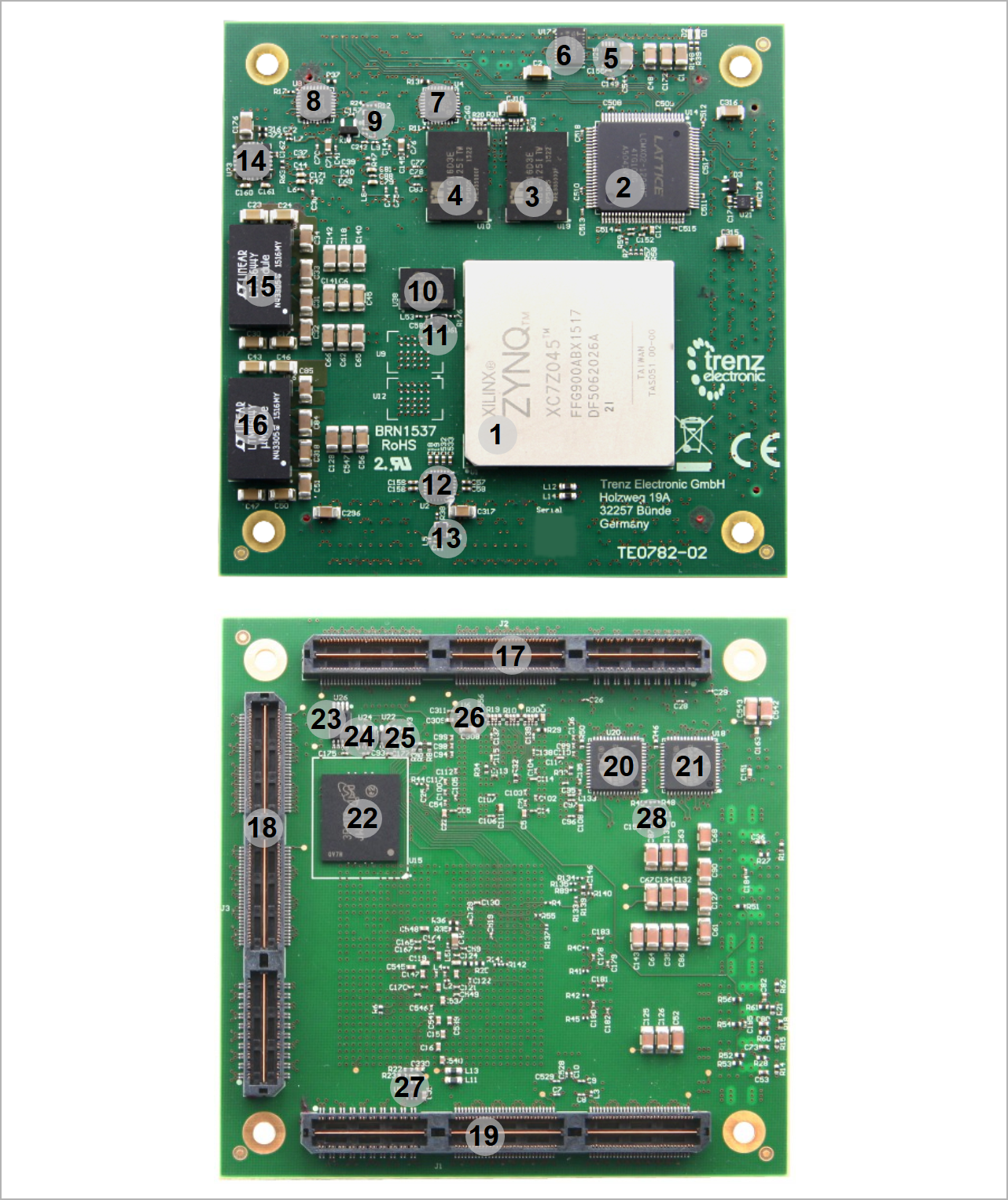
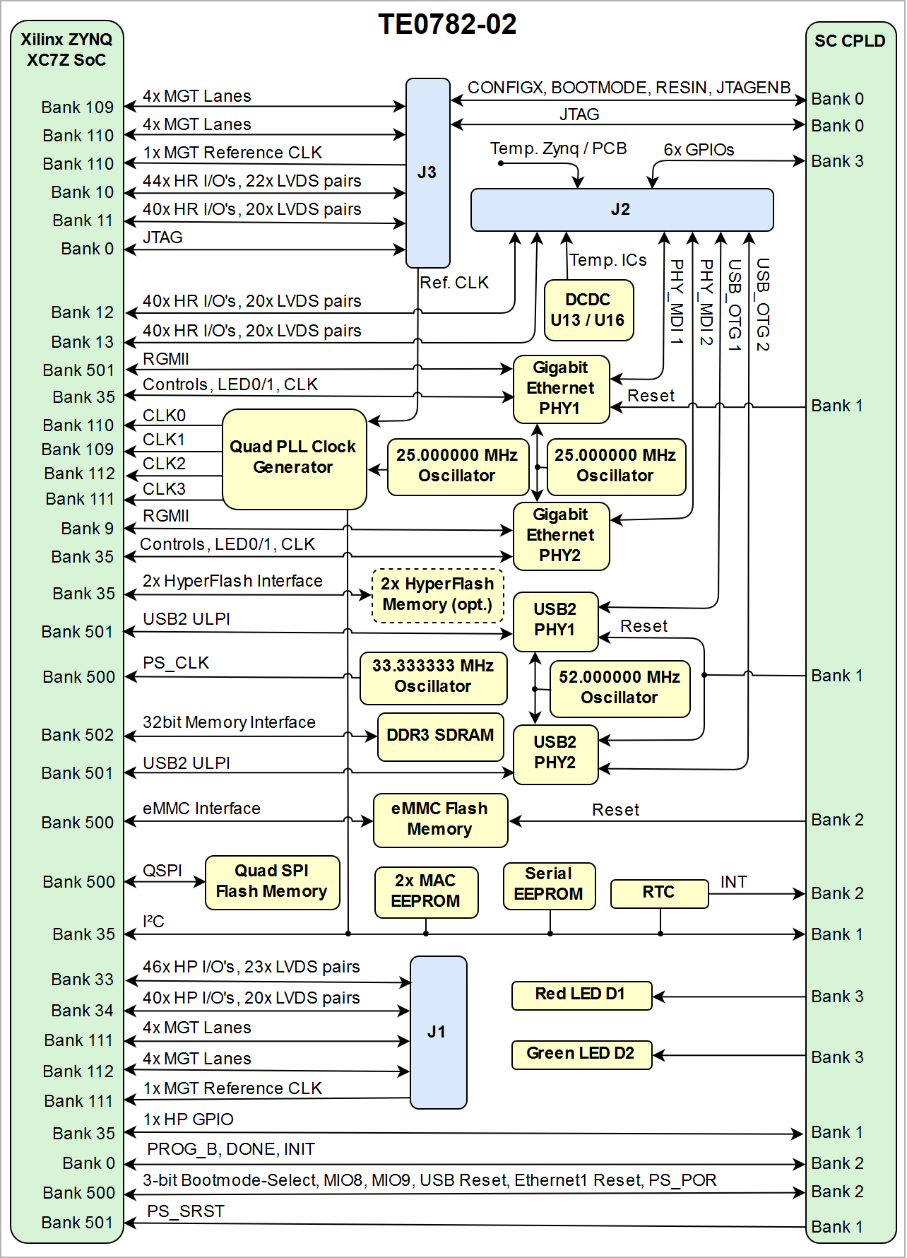
- Xilinx Zynq UltraScale+ MPSoC-7000 SoC, U1
- Lattice Semiconductor MachXO2 1200HC CPLD, U14
- 4Gbit DDR3L SDRAM, U19
- 4Gbit DDR3L SDRAM, U10
- I²C voltage translator, U25
- Intersil ISL12020MIRZ Real Time Clock, U17
- Microchip USB3320C USB PHY transceiver, U4
- Microchip USB3320C USB PHY transceiver, U8
- SiTime SiT8008 52.000000 MHz oscillator, U7
- 32 MByte QSPI Flash memory, U38
- SiTime SiT8008 33.333333 MHz oscillator, U61
- SI5338A programmable quad PLL clock generator, U2
- SiTime SiT8008 25.000000 MHz oscillator, U3
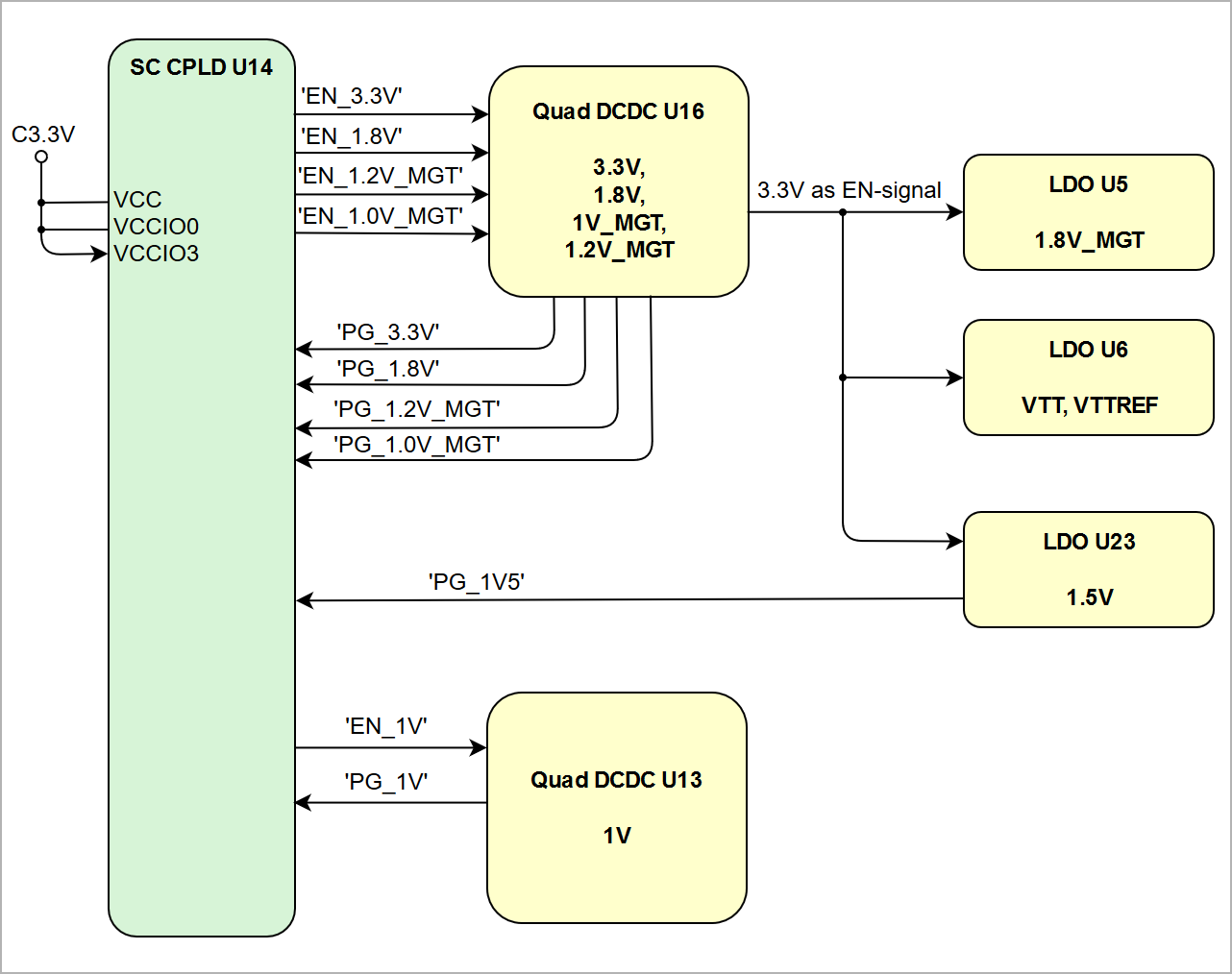
- TPS74801 LDO @1.5V, U23
- LT quad 4A PowerSoC DC-DC converter (@1.0V), U13
- LT quad 4A PowerSoC DC-DC converter (@3.3V, @1,8V, @1.2V_MGT, @1.0V_MGT), U16
- Samtec ASP-122952-01 160-pin stacking strip (2 rows a 80 positions), J2
- Samtec ASP-122952-01 160-pin stacking strip (2 rows a 80 positions), J3
- Samtec ASP-122952-01 160-pin stacking strip (2 rows a 80 positions), J1
- Marvell Alaska 88E1512 Gigabit Ethernet PHY, 20
- Marvell Alaska 88E1512 Gigabit Ethernet PHY, U18
- Micron Technology 4 GByte eMMC, U15
- Microchip 128Kbit I²C EEPROM, U26
- Microchip 2Kbit I²C MAC EEPROM, U24
- Microchip 2Kbit I²C MAC EEPROM, U22
- TPS51206 DDR reference voltage and termination regulator, U6
- TPS799 LDO @1.8V_MGT, U5
- SiTime SiT8008 25.000000 MHz oscillator, U11
...
4 of the 7 boot mode strapping pins (MIO2 ... MIO8) of the Xilinx Zynq-7000 SoC device are hardware programmed on the board, 3 of them are set be by the SC CPLD firmware. They The boot strapping pins are evaluated by the Zynq device soon after the 'PS_POR' signal is deasserted to begin the boot process (see section "Boot Mode Pin Settings" of Xilinx manual UG585).
The TE0782 board is programmed in the SC CPLD firmware to boot initially from the on-board QSPI Flash memory U38. See section Bootmode in the TE0782 SC CPLD reference Wiki page.
...
The Xilinx Zynq-7000 SoC used on the TE0782 module has 16 MGT transceiver lanes. All of them are wired directly to B2B connectors J1 and J3. MGT (Multi Gigabit Transceiver) lane consists of one transmit and one receive (TX/RX) differential pairs, four signals total per one MGT lane with data transmission rates up to 12.5Gb/s per lane (Xilinx GTX transceiver). Following table lists lane number, FPGA bank number, transceiver type, signal schematic name, board-to-board pin connection and FPGA pins connection:
Board to
| Bank | Type | Lane | Signal Name | B2B Pin | FPGA Pin |
|---|---|---|---|---|---|
| 109 | GTX | 0 |
|
|
|
| 1 |
|
|
| ||
| 2 |
|
|
| ||
| 3 |
|
|
| ||
| 110 | GTX | 0 |
|
|
|
| 1 |
|
|
| ||
| 2 |
|
|
| ||
| 3 |
|
|
| ||
| 111 | GTX | 0 |
|
|
|
| 1 |
|
|
| ||
| 2 |
|
|
| ||
| 3 |
|
|
| ||
| 112 | GTX | 0 |
|
|
|
| 1 |
|
|
| ||
| 2 |
|
|
| ||
| 3 |
|
|
|
...
eMMC Flash memory device (U15) is connected to the Zynq PS MIO bank 500 pins MIO10..MIO15. eMMC chips MTFC4GMVEA-4M IT (Flash NAND-IC 2x 16 Gbit) is used with 4 GByte of memory density.
...
DDR3L Memory
By default TE0782-02 module has two 16-bit wide IM (Intelligent Memory) IM4G16D3FABG-125I DDR3L SDRAM (DDR3-1600 Speedgrade) chips (U10, U19) arranged into 32-bit wide memory bus providing total of 1 GBytes of on-board RAM.
...
Two quad SPI compatible serial bus flash memory for FPGA configuration file storage is provided by Spansion S25FL256SAGBHI20 (U38) with 256 Mbit (32 MByte) memory density. After configuration completes the remaining free memory can be used for application data storage. All four SPI data lines are connected to the FPGA allowing x1, x2 or x4 data bus widths to be used. The maximum data transfer rate depends on the bus width and clock frequency.
...
| Scroll Title | ||||||||||||||||||||||||||||||||
|---|---|---|---|---|---|---|---|---|---|---|---|---|---|---|---|---|---|---|---|---|---|---|---|---|---|---|---|---|---|---|---|---|
| ||||||||||||||||||||||||||||||||
|
...
Board to Board Connectors
The TE0782 SoM has three 160-pin double-row ASP-122952-01 Samtec connectors on the bottom side which mate with ASP-122953-01 Samtec connectors on the baseboard. Mating height is 5 mm.Include Page 8.5 x 8.5 SoM QSH and QTH B2B Connectors 8.5 x 8.5 SoM QSH and QTH B2B Connectors
Variants Currently In Production
...
Parameter | Min | Max | Units | Notes |
|---|---|---|---|---|
VIN supply voltage | -0.3 | 15 | V | LTM4644 datasheet |
| C3.3V supply voltage | -0.3 | 3.6 | V | LTM4644 datasheet |
| VBAT supply voltage | -0.3 | 6 | V | TPS780180 datasheet |
| PS I/O supply voltage, VCCO_PSIO | -0.5 | 3.6 | V | Xilinx document DS191 |
| PS I/O input voltage | -0.4 | VCCO_PSIO + 0.55 | V | Xilinx document DS191 |
| HP I/O bank supply voltage, VCCO | -0.5 | 2.0 | V | Xilinx document DS191 |
| HP I/O bank input voltage | -0.55 | VCCO + 0.55 | V | Xilinx document DS191 |
| HR I/O bank supply voltage, VCCO | -0.5 | 3.6 | V | Xilinx document DS191 |
| HR I/O bank input voltage | -0.55 | VCCO + 0.55 | V | Xilinx document DS191 |
| Reference Voltage pin | -0.5 | 2 | V | Xilinx document DS191 |
| Differential input voltage | -0.4 | 2.625 | V | Xilinx document DS191 |
| MGT reference clocks absolute input voltage | -0.5 | 1.32 | V | Xilinx document DS191 |
| MGT absolute input voltage | -0.5 | 1.26 | V | Xilinx document DS191 |
Voltage on SC CPLD pins | -0.5 | 3.75 | V | Lattice Semiconductor MachXO2 datasheet |
Storage temperature | -40 | +85 | °C | See eMMC MTFC4GMVEA datasheet |
...
| Parameter | Min | Max | Units | Notes |
|---|---|---|---|---|
| VIN supply voltage | 11.4 | 1412.6 | V | See LTM4644 datasheet, 12V nominal |
| C3.3V supply voltage | 3.3 | 3.465 | V | See LCMXO2-256HC, LTM4644 datasheet |
| VBAT supply voltage | 2.2 | 5.5 | V | TPS780180 datasheet |
| PS I/O supply voltage, PS I/O supply voltage, VCCO_PSIO | 1.710 | 3.465 | V | Xilinx document DS191 |
| PS I/O input voltage | –0.20 | VCCO_PSIO + 0.20 | V | Xilinx document DS191 |
| HP I/O banks supply voltage, VCCO | 1.14 | 1.89 | V | Xilinx document DS191 |
| HP I/O banks input voltage | -0.20 | VCCO + 0.20 | V | Xilinx document DS191 |
| HR I/O banks supply voltage, VCCO | 1.14 | 3.465 | V | Xilinx document DS191 |
| HR I/O banks input voltage | -0.20 | VCCO + 0.20 | V | Xilinx document DS191 |
| Differential input voltage | -0.2 | 2.625 | V | Xilinx document DS191 |
| Voltage on SC CPLD pins | -0.3 | 3.6 | V | Lattice Semiconductor MachXO2 datasheet |
| Operating Temperature Range | -40 | 85 | °C | Xilinx document DS191, industrial grade Zynq temperarure range |
...
| HTML |
|---|
<!-- Generate new entry: 1.add new row below first 2.Copy "Page Information Macro(date)" Macro-Preview, Metadata Version number, Author Name and description to the empty row. Important Revision number must be the same as the Wiki document revision number 3.Update Metadata = "Page Information Macro (current-version)" Preview+1 and add Author and change description. --> |
Document Change History
| Date | Revision | Contributors | Description | ||||||||||||||||||||||||||
|---|---|---|---|---|---|---|---|---|---|---|---|---|---|---|---|---|---|---|---|---|---|---|---|---|---|---|---|---|---|
|
|
|
| ||||||||||||||||||||||||||
| 2018-07-20 | v.33 | John Hartfiel |
| ||||||||||||||||||||||||||
2018-07-19 | v.32 | Ali Naseri |
| ||||||||||||||||||||||||||
| 2018-05-15 | v.22v22 | Ali Naseri |
| ||||||||||||||||||||||||||
| 2018-01-31 | Ali Naseri |
| |||||||||||||||||||||||||||
| 2017-06-07 | Jan Kumann |
| |||||||||||||||||||||||||||
| 2017-05-23 | v.13V13 | Jan Kumann |
| ||||||||||||||||||||||||||
| 2017-01-24 | V12v.12 | Ali Naseri |
| ||||||||||||||||||||||||||
| 2016-06-27 | v10v.10 | Ali Naseri, Jan Kumann |
| ||||||||||||||||||||||||||
| -- | all |
|
|
Disclaimer
| Include Page | ||||
|---|---|---|---|---|
|
Overview
Content Tools