Page History
...
| HTML |
|---|
<!-- Template Revision 1.4 beta (HTML comment will not display, it's not needed to remove them. For Template/Skeleton changes, increase Template Revision number. So we can check faster, if the TRM style is up to date) --> |
| Scroll Ignore |
|---|
Download PDF version of this document. |
| Scroll pdf ignore | |
|---|---|
Table of Contents
|
...
- Xilinx Zynq UltraScale+ MPSoC 784 pin package (options: ZU2CG, ZU2EG, ZU3CG, ZU3EG, ZU4CG, ZU4EV)
- Memory
- 64-Bit DDR4, 8 GByte maximum
- Dual SPI boot Flash in parallel, 512 128 MByte maximum - User I/O
- 65 x MIO, 48 x HD (all), 156 x HP (3 banks)
- Serial transceiver: 4 x GTR (+ 4 x GTH transceiver with ZU4CG or ZU4EV MPSoC)
- Transceiver clocks inputs and outputs
- PLL clock generator inputs and outputs - Size: 52 x 76 mm, 3 mm mounting holes for skyline heat spreader
- B2B connectors: 4 x 160 pin
- Si5338A - 4 output PLL
- All power supplies on board, single 3.3V power source required
- LP, FP, PL separately controlled power domains - Support for all boot modes (except NAND) and scenarios
- Support for any combination of PS connected peripherals
...
- Xilinx ZYNQ UltraScale+ MPSoC, U1
- 2-Input AND Gate, U39
- Red LED (DONE), D1
- 256Mx16 DDR4-2400 SDRAM, U12
- 256Mx16 DDR4-2400 SDRAM, U9
- 256Mx16 DDR4-2400 SDRAM, U2
- 256Mx16 DDR4-2400 SDRAM, U3
- 12A PowerSoC DC-DC converter, U4 (either TPS548A28RWWR or MPQ8633BGLE-Z is assembled which is up to Trenz Electronic GmbH)
- 1.5A LDO DC-DC converter, U10
- 1.5A LDO DC-DC converter, U8
- Voltage monitor circuit, U41
- 0.35A LDO DC-DC converter, U26
- 0.35A LDO DC-DC converter, U27
- Ultra fine 0.50 mm pitch, Razor Beam™ LP Slim Terminal Strip with 160 contacts, J3
- Ultra fine 0.50 mm pitch, Razor Beam™ LP Slim Terminal Strip with 160 contacts, J1
- Ultra fine 0.50 mm pitch, Razor Beam™ LP Slim Terminal Strip with 160 contacts, J4
- Ultra fine 0.50 mm pitch, Razor Beam™ LP Slim Terminal Strip with 160 contacts, J2
- 4-channel programmable PLL clock generator, U5
- Low-power programmable oscillator @ 25.000000 MHz, U5
- Low-power programmable oscillator @ 33.333333 MHz (PS_CLK), U32
- 256 Mbit serial NOR Flash memory, U7
- 256 Mbit serial NOR Flash memory, U17
...
| Storage device name | Content | Notes |
|---|---|---|
User configuration EEPROMs with MAC address (1x Microchip 24LC128-I/ST, 3x Microchip 24AA025E48T-I/OT) | Not programmed | available since PCB REV02 |
SPI Flash main array | Not programmed | - |
eFUSE Security | Not programmed | - |
| Si5338A programmable PLL NVM OTP | Not programmed- | Only volatile memory is programmable of field. NVM can't be program on field. Custom assembly variant with preprogrammed NVM is possible on request |
Table 1: Initial Delivery State of the flash memories
...
| Bank | Type | B2B Connector | Count of MGT Lanes | Schematic Names / Connector Pins | MGT Bank's Reference Clock Inputs |
|---|---|---|---|---|---|
2241) | GTH | J1 | 4 GTH lanes (4 RX / 4TX) | B224_RX3_P, B224_RX3_N, pins J1-51, J1-53 B224_RX2_P, B224_RX2_N, pins J1-57, J1-59 B224_RX1_P, B224_RX1_N, pins J1-63, J1-65 B224_RX0_P, B224_RX0_N, pins J1-69, J1-71 | 1 reference clock signal (B224_CLK0) from B2B connector 1 reference clock signal (B224_CLK1) from programmable |
| 505 | GTR | J2 | 4 GTR lanes (4 RX / 4TX) | B505_RX3_P, B505_RX3_N, pins J2-5154, J2-4952 B505_RX2_P, B505_RX2_N, pins J2-5760, J2-5558 B505_RX1_P, B505_RX1_N, pins J2-6366, J2-6164 B505_RX0_P, B505_RX0_N, pins J2-6972, J2-6770 | 2 reference clock signals (B505_CLK0, B505_CLK1) from B2B connector 2 reference clock signals (B505_CLK2, B505_CLK3) from programmable |
...
The TE0803 SoM can be configured with max. 512 MByte Flash memory for configuration and operation. Flash size and type depends on assembly version.
| Name | IC | Designator | PS7 | MIO | Notes |
|---|---|---|---|---|---|
| SPI FlashN25Q256A11E1240E | U7 | QSPI0 | MIO0 ... MIO5 | Dual parallel booting possible, 32 MByte memory per Flash IC at standard configuration | |
| SPI FlashN25Q256A11E1240E | U17 | QSPI0 | MIO7 ... MIO12 | As above |
...
The TE0803-01 SoM is equipped with with four DDR4-2400 SDRAM modules chips with up to 8 GByte of memory. The SDRAM modules chips are connected to the Zynq MPSoC's PS DDR controller (bank 504) via 64-bit wide data bus.
Refer to the Xilinx Zynq UltraScale+ datasheet DS925 for more information, if the specific Zynq UltraScale+ MPSoC chip on module supports the maximum data transmission rate of 2400 MByte/s.
Programmable PLL Clock Generator
Following table illustrates on-board Si5338A programmable clock multiplier chip inputs and outputs:
Configuration EEPROM
The TE0803 (PCB REV02 or newer) contains EEPROMs for general user purposes and mac address. The EEPROMs are provided by Microchip and all have I²C interfaces:
| EEPROM Modell | Schematic Designator | Memory Density | Purpose |
|---|---|---|---|
| 24AA025E48T-I/OT | U41 | 2 Kbit | user |
Table 21: On-board configuration EEPROMs overview
Programmable PLL Clock Generator
Following table illustrates on-board Si5338A programmable clock multiplier chip inputs and outputs:
| Input | Input | Connected to | Frequency | Notes |
|---|---|---|---|---|
| IN1 / IN2 | B2B Connector pins J2-4, J2-6 (differential pair) | User | AC decoupling required on base | |
| IN3 | On-board Oscillator (U6) | 25.000000 MHz | - | |
| Output | Connected to | Frequency | Notes | |
| CLK0 A/B | B2B Connector pins J2-1, J2-3 (differential pair) | User | Default off | |
| CLK1 A/B | B224 CLK1 (only available at ZU5EV MPSoC with ZU4 and higher ) | User | Default off | |
| CLK2 A/B | B505 CLK3 | User | Default off | |
| CLK3 A/B | B505 CLK2 | User | Default off |
...
Table 12: B2B connector pin-out of Si5338A control interface
| Note |
|---|
Si5338A OTP ROM Si5338A NVM is not programmed by default at delivery, so it . It is customers responsibility to either configure Si5338A volatile memory during FSBL or then use Silicon Labs programmer and burn the OTP ROM with customer fixed clock setup. |
...
. Custom assembly variant with preprogrammed NVM is possible on request. |
Refer to Si5338A datasheet for more information.
...
Figure 3: Power Distribution Diagram (For U4 either TPS548A28RWWR or MPQ8633BGLE-Z is assembled which is up to Trenz Electronic GmbH)
| Note |
|---|
Current rating of Samtec Razor Beam LP Terminal/Socket Strip ST5/SS5 B2B connectors is 1.5 A per pin (1 pin powered per row). |
...
| Voltages on B2B Connectors | B2B J1 Pin | B2B J2 Pin | B2B J3 Pin | B2B J4 Pin | Input/ Output | Note |
|---|---|---|---|---|---|---|
| PL_DCIN | J1-151, J1-153,J1-155, J1-157, J1-159 | - | - | - | Input | - |
| DCDCIN | - | J2-154, J2-156, J2-158, J2-160, J2-153, J2-155, J2-157, J2-159 | - | - | Input | - |
| LP_DCDC | - | J2-138, J2-140, J2-142, J2-144 | - | - | Input | - |
| PS_BATT | - | J2-125 | - | - | Input | - |
| GT_DCDC | - | - | J3-157, J3-158, J3-159, J3-160 | - | Input | - |
| PS_1V8 | - | J2-99 | J3-147, J3-148 | - | Output | Internal voltage level 1.8V nominal output |
| PL_1V8 | J1-91, J1-121 | - | - | - | Output | Internal voltage level 1.8V nominal output |
| DDR_1V2 | - | J2-135 | - | - | Output | Internal voltage level 1.2V nominal output |
...
| Parameter | Min | Max | Unit | Notes / Reference Document |
|---|---|---|---|---|
| PL_DCIN | -0.3 | 74 | V | TPS82085SIL / EN63A0QI data sheet / Limit is LP_DCDC over EN/PG |
| DCDCIN | -0.3 | 74 | V | TPS82085SIL TPS82085SIL / TPS51206PSQ data sheet / Limit is LP_DCDC over EN/PG |
| LP_DCDC | -0.3 | 4 | V | TPS3106K33DBVR data sheet |
| GT_DCDC | -0.3 | 74 | V | TPS82085SIL data sheet / Limit is LP_DCDC over EN/PG |
| PS_BATT | -0.5 | 2 | V | Xilinx DS925 data sheet |
| VCCO for HD I/O banks | -0.5 | 3.4 | V | Xilinx DS925 data sheet |
| VCCO for HP I/O banks | -0.5 | 2 | V | Xilinx DS925 data sheet |
| VREF | -0.5 | 2 | V | Xilinx DS925 data sheet |
| I/O input voltage for HD I/O banks | -0.55 | VCCO + 0.55 | V | Xilinx DS925 data sheet |
| I/O input voltage for HP I/O banks | -0.55 | VCCO + 0.55 | V | Xilinx DS925 data sheet |
| PS I/O input voltage (MIO pins) | -0.5 | VCCO_PSIO + 0.55 | V | Xilinx DS925 data sheet, VCCO_PSIO 1.8V nominally |
| Receiver (RXP/RXN) and transmitter (TXP/TXN) absolute input voltage | -0.5 | 1.2 | V | Xilinx DS925 data sheet |
| Voltage on input pins of NC7S08P5X 2-Input AND Gate | -0.5 | VCC + 0.5 | V | NC7S08P5X data sheet, see schematic for VCC |
| Voltage on input pins (nMR) of TPS3106K33DBVR Voltage Monitor, U41 | -0.3 | VDD + 0.3 | V | TPS3106 data sheet, VDD = LP_DCDC |
| "Enable"-signals on TPS82085SIL ('EN_LPD') | -0.3 | 7 | V | TPS82085SIL data sheet |
| Storage temperature (ambient) | -40 | 100 | °C | ROHM Semiconductor SML-P11 Series data sheet |
...
| Parameter | Min | Max | Unit | Notes / Reference Document |
|---|---|---|---|---|
| PL_DCIN | 23.53 | 3.6 | V | EN63A0QI / TPS82085SIL data sheet / Limit is LP_DCDC over EN/PG |
| DCDCIN | 3.13 | 3.6 | V | TPS82085SIL / TPS51206PSQ data sheet / Limit is LP_DCDC over EN/PG |
| LP_DCDC | 23.53 | 3.6 | V | TPS82085SIL / TPS3106K33DBVR data sheet |
| GT_DCDC | 23.53 | 3.6 | V | TPS82085SIL data sheet / Limit is LP_DCDC over EN/PG |
| PS_BATT | 1.2 | 1.5 | V | Xilinx DS925 data sheet |
| VCCO for HD I/O banks | 1.14 | 3.4 | V | Xilinx DS925 data sheet |
| VCCO for HP I/O banks | 0.95 | 1.9 | V | Xilinx DS925 data sheet |
| I/O input voltage for HD I/O banks. | -0.2 | VCCO + 0.2 | V | Xilinx DS925 data sheet |
| I/O input voltage for HP I/O banks | -0.2 | VCCO + 0.2 | V | Xilinx DS925 data sheet |
| PS I/O input voltage (MIO pins) | -0.2 | VCCO_PSIO + 0.2 | V | Xilinx DS925 data sheet, VCCO_PSIO 1.8V nominally |
| Voltage on input pins of NC7S08P5X 2-Input AND Gate | 0 | VCC | V | NC7S08P5X data sheet, see schematic for connected VCCs |
| Voltage on input pins (MR) of TPS3106K33DBVR Voltage Monitor, U41 | 0 | VDD | V | TPS3106 data sheet, VDD = LP_DCDC |
...
Operating Temperature Ranges
Extended grade: 0°C to +100°C.
The module operating temperature range depends also on customer design and cooling solution. Please contact us for options.
...
- Module size: 52 mm × 76 mm. Please download the assembly diagram for exact numbers
- Mating height with standard connectors: 4mm5mm
- PCB thickness: 1.6mm
- Highest part on PCB: approx. 3mm. Please download the step model for exact numbers
...
| Date | Revision | Notes | Link to PCN | Documentation Link |
|---|---|---|---|---|
| 2019- | 12-2301 | First production release | - | TE0803-01 |
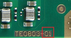
Hardware revision number is written on the PCB board together with the module model number separated by the dash.
Document Change History
| 03-18 | 03 |
| TE0803 Product Change Notifications | TE0803-03 |
| 2018-07-19 | 02 |
| TE0803 Product Change Notifications | TE0803-02 |
| 2016-12-23 | 01 | First production release | - | TE0803-01 |
Hardware revision number is written on the PCB board together with the module model number separated by the dash.
Document Change History
| Date | Revision | Contributors | Description | ||||||||||||||||||||||||
|---|---|---|---|---|---|---|---|---|---|---|---|---|---|---|---|---|---|---|---|---|---|---|---|---|---|---|---|
|
|
|
| ||||||||||||||||||||||||
| 22-02-25 | v.50 | John Hartfiel |
| ||||||||||||||||||||||||
| 22-02-08 | v.46 | John Hartfiel |
| ||||||||||||||||||||||||
| 2021-05-17 | v.41 | John Hartfiel |
| ||||||||||||||||||||||||
| 2021-03-11 | v.40 | John Hartfiel |
| ||||||||||||||||||||||||
| 2019-07-15 | v.36 | John Hartfiel |
| ||||||||||||||||||||||||
| 2019-07-02 | v.35 | John Hartfiel |
| ||||||||||||||||||||||||
| 2019-06-19 | v.33 | John Hartfiel |
| ||||||||||||||||||||||||
2018-08-20 | v.29 | ||||||||||||||||||||||||||
| Date | Revision | Contributors | Description | ||||||||||||||||||||||||
| Page info | modified-date | modified-date | |||||||||||||||||||||||||
| dateFormat | yyyy-MM-dd |
| John Hartfiel |
| |||||||||||||||||||||||
2018-08-06 | v.28 | John Hartfiel |
| ||||||||||||||||||||||||
| 2017-11-13 | v.23 | Ali Naseri |
| ||||||||||||||||||||||||
2017-11-13 | v.19 | John Hartfiel |
| ||||||||||||||||||||||||
| 2017-10-19 | v.18 | John Hartfiel |
| ||||||||||||||||||||||||
| 2017-08-15 | v.17 | Vitali Tsiukala |
| ||||||||||||||||||||||||
2017-08-07 | v.14 | Jan Kumann |
| ||||||||||||||||||||||||
2017-05-17 | V.4 | Ali Naseri | Current TRM release. | ||||||||||||||||||||||||
| 2017-05-10 | v.1 | Ali Naseri | Initial document. |
...
Overview
Content Tools