nearly the same like TEBB0714: TEBB0714 TRM
| Page properties |
|---|
|
Template Revision 2.12
- Module: TRM Name always "TE Series Name" +TRM
Example: "TE0728 TRM" - Carrier: TRM Name usually "TEB Series Name" +TRM
Example: "TEB0728 TRM"
|
...
The Trenz Electronic TEBA0714 is a carrier for Trenz Electronic module TE0714 which is an industrial - grade ... module ... based on Xilinx ...module integrated with Xilinx Artix 7.
Refer to http://trenz.org/teba0714-info for the current online version of this manual and other available documentation.
| Page properties |
|---|
|
Notes :- short description of the PCB
- Short Link of the wiki resources reference:
|
Key Features
| Page properties |
|---|
|
Note:
'description: Important components and connector or other Features of the module
→ please sort and indicate assembly optionsKey optionsKey Features' must be split into 6 main groups:- FPGA/Module
- Package:
- Speed:
- Temperature:
- RAM/Storage
- On Board
- Interface
- E.g. ETH, USB, B2B, Display port
- Power
- E.g. Input supply voltage
- Dimension
|
- Module:
- Trenz TE0714 Modulsockel (2x Samtec 100 Pin LSHM-Serienstecker)
- Speed:
- Temperature:
- On Board:
- 2 x User LEDs (rot/grünRed, Green)
- 1 x PROG_ DONE LED (rotRed)
- Interface:
- 2 x Pin - Header 50 polig 50 Pol. (FPGA Bank Ein- und Ausgänge und StromversorgungI/Os and Power)
- 2x Samtec 100 Pin LSHM Series Connectors
- 1 x XMOD JTAG/UART Adapter (TE0790)
- 1 x Pin -Header für FPGA Bank Stromversorgung VCCIO34 (1.8 VOUT, 2.5V, 3.3 VOUTHeader 16 Pol. (JTAG, MGT-CLK, Boot Mode, XADC, I/O's)
- 1 x Pin - Header für FPGA Bank Stromversorgungr V_CFG (1.8 VOUT, 2.5V, 3.3 VOUT)
- 1 x XMOD (TE0790) Pin-Header
- 1 x Pin-Header 16 polig (JTAG, MGT-CLK, Boot Mode, XADC, I/O's)
- 1 x Pin-Header 10 polig (Ein-/ und Ausgänge)
- 10 Pol. (FPGA Bank I/Os and Power)
- 1 x SFP+ Connectors1 x SFP-Anschluss
- Power:
- 1 x LDO Spannungsregler Regulator
- 3.3 V auf 2.5 V3V Nominal Power supply
- Dimension: 30 mm x 40
Block Diagram
| Page properties |
|---|
|
add drawIO object here.
|
| Scroll Title |
|---|
| anchor | Figure_OV_BD |
|---|
| title | TEBA0714 block diagram |
|---|
|
| Scroll Ignore |
|---|
| draw.io Diagram |
|---|
| border | truefalse |
|---|
| viewerToolbar | true |
|---|
| |
|---|
| fitWindow | false |
|---|
| diagramDisplayName | |
|---|
| lbox | true |
|---|
| revision | 12 |
|---|
| diagramName | TEBA0714_OV_BD |
|---|
| simpleViewer | false |
|---|
| width |
|---|
| diagramWidth | 641 |
|---|
| | links | auto |
|---|
| tbstyle | hidden |
|---|
| diagramWidth | 639 | revision | 3 |
|---|
|
|
| Scroll Only |
|---|
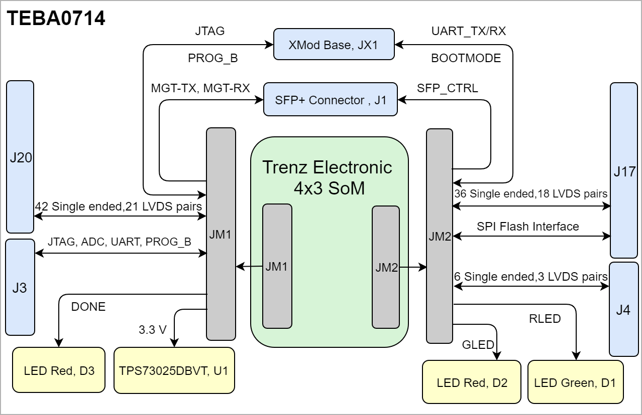 Image Modified Image Modified |
|
Main Components
| Page properties |
|---|
|
Notes :- Picture of the PCB (top and bottom side) with labels of important components
- Add List below
|
| Scroll Title |
|---|
| anchor | Figure_OV_MC |
|---|
| title | TEBA0714 main components |
|---|
|
| Scroll Ignore |
|---|
| draw.io Diagram |
|---|
| border | truefalse |
|---|
| viewerToolbar | true |
|---|
| |
|---|
| fitWindow | false |
|---|
| diagramDisplayName | |
|---|
| lbox | true |
|---|
| revision | 6 |
|---|
| diagramName | TEBA0714_OV_MC |
|---|
| simpleViewer | false |
|---|
| width | |
|---|
| links | auto |
|---|
| tbstyle | hidden |
|---|
| diagramWidth | 641 | revision | 2 |
|---|
|
|
| Scroll Only |
|---|
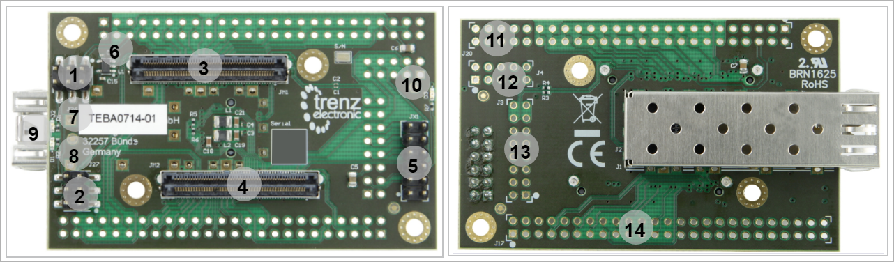 Image Modified Image Modified |
|
- ...
- ...
- ...
Initial Delivery State
- SMT pin header, J26
- SMT pin header, J27
- Board to Board (B2B) Connector, JM1
- Board to Board (B2B) Connectorr, JM2
- XMOD header, JX1
- Voltage Regulator, U1
- User Red LED, D2
- User Green LED, D1 (Red)
- SFP+ Connector, J1
- User Red LED, D3
- 50 pin header (Not assembled), J20
- 16 pin header (Not assembled), J3,
- 10-pin header (Not assembled), J4
- 50-pin header (Not assembled), J17
Initial Delivery State
| Page properties |
|---|
|
| Notes : |
| Page properties |
|---|
|
Notes : Only components like EEPROM, QSPI flash and DDR3 can be initialized by default at manufacture.If there is no components which might have initial data ( possible on carrier) you must keep the table empty |
| Scroll Title |
|---|
| anchor | Table_OV_IDS |
|---|
| title | Initial delivery state of programmable devices on the module |
|---|
|
| Scroll Table Layout |
|---|
| orientation | portrait |
|---|
| sortDirection | ASC |
|---|
| repeatTableHeaders | default |
|---|
| style | |
|---|
| widths | |
|---|
| sortByColumn | 1 |
|---|
| sortEnabled | false |
|---|
| cellHighlighting | true |
|---|
|
| Storage device name | Content | Notes | Quad SPI Flash | EEPROM | DDR3 SDRAM |
|---|
| --- | --- | --- | System Controller CPLD |
|
Configuration Signals
| Page properties |
|---|
|
- Overview of Boot Mode, Reset, Enables.
|
...
| Scroll Title |
|---|
| anchor | Table_OV_BP |
|---|
| title | Boot process. |
|---|
|
| Scroll Table Layout |
|---|
| orientation | portrait |
|---|
| sortDirection | ASC |
|---|
| repeatTableHeaders | default |
|---|
| style | |
|---|
| widths | |
|---|
| sortByColumn | 1 |
|---|
| sortEnabled | false |
|---|
| cellHighlighting | true |
|---|
|
| Signal | MODE Signal State | Boot Mode | Note |
|---|
| BOOTMODE | 0 | Slave SelectMAP |
| | 1 | Master SPI |
|
|
| Scroll Title |
|---|
| anchor | Table_OV_RST |
|---|
| title | Reset process. |
|---|
|
| Scroll Table Layout |
|---|
| orientation | portrait |
|---|
| sortDirection | ASC |
|---|
| repeatTableHeaders | default |
|---|
| style | |
|---|
| widths | |
|---|
| sortByColumn | 1 |
|---|
| sortEnabled | false |
|---|
| cellHighlighting | true |
|---|
|
I/O| Signal State | Note |
|---|
| PROG_B | JM1-94 | Active Low | Clear FPGA configuration and initiate a new configuration |
|
Signals, Interfaces and Pins
| Page properties |
|---|
|
Notes :- For carrier or stand-alone boards use subsection for every connector type (add designator on description, not on the subsection title), for example:
- For modules which needs carrier use only classes and refer to B2B connector if more than one is used, for example
|
Board to Board (B2B) I/Os
FPGA bank number and number Number of I/O signals and Interfaces connected to the B2B connector:
| Scroll Title |
|---|
| anchor | Table_SIP_B2B |
|---|
| title | General PL I/O to B2B connectors information |
|---|
|
| Scroll Table Layout |
|---|
| orientation | portrait |
|---|
| sortDirection | ASC |
|---|
| repeatTableHeaders | default |
|---|
| style | |
|---|
| widths | |
|---|
| sortByColumn | 1 |
|---|
| sortEnabled | false |
|---|
| cellHighlighting | true |
|---|
|
| FPGA Bank | B2B Connector | Interface | Number of I/O Signal Count | Voltage Level | Notes |
|---|
|
...
JTAG access to the TExxxx SoM through B2B connector JMX.
...
| anchor | Table_SIP_JTG |
|---|
| title | JTAG pins connection |
|---|
...
JTAG Signal
...
B2B Connector
...
JM1
| User I/O | 52 Single ended, 27 Differential | - | | MGT lanes | 4 Differential, 2 lanes |
| | MGT reference clock input | 2 Single ended, 1 Differential |
| | JTAG | 4 Single ended |
| | SoM control signals | 2 Single ended | PROG_B, DONE | | JM2 | User I/O | 36 Single ended or 18 differential | - | | SFP+ Interface control signals | 8 Single ended |
| | QSPI interface | 6 Single ended |
| | UART interface | 2 Single ended |
| | User LEDs | 2 Single ended | Red, Green | | SoM control signals | 1 Single ended | BOOTMODE |
|
TEBA0714 is equipped with four pin headers J17, J20, J3 and J4 which are not assembled on the board, in case of need customer can solder the pins and have access to the signals in the following table.
| Scroll Title |
|---|
| anchor | Table_SIP_PinHeader |
|---|
| title | General I/O to Pin headers information |
|---|
|
| Scroll Table Layout |
|---|
| orientation | portrait |
|---|
| sortDirection | ASC |
|---|
| repeatTableHeaders | default |
|---|
| style | |
|---|
| widths | |
|---|
| sortByColumn | 1 |
|---|
| sortEnabled | false |
|---|
| cellHighlighting | true |
|---|
|
| Pin Header | Interface | Number of I/O | Notes |
|---|
J17
| User I/O | 36 Single ended, 18 Differential | Module FPGA Bank 14 | | SPI interface | 6 Single ended | - | | Power | 4 Single ended | 3.3V, V_CFG | | J20 | User I/O | 42 Single ended or 21 differential | Module FPGA Bank 34 | | Power | 4 Single ended | 3.3V, V_CFG | | User LEDs | 2 Single ended | Red, Green | | SoM control signals | 1 Single ended | 'BOOTMODE' | | J3 | JTAG | 4 Single ended |
| | UART | 2 Single ended | B14_L25, B14_L0 | | ADC | 2 Single ended |
| | Clock | 2 Single ended, 1 Differential |
| | Power | 4 Single ended | 3.3V, V_CFG | | Control Signals | 2 Single ended | BOOTMODE, PROG_B | | J4 | User I/O | 6 Single ended or 3 differential |
| | Power | 2 Single ended | 3.3V, 3.3V_OUT |
|
JTAG Interface Base
JTAG access to the mounted SoM is provided through B2B connector JM1 and JM2 and is also routed to the XMOD JTAG/UART header JX1.
MIO Pins
| Page properties |
|---|
|
you must fill the table below with group of MIOs which are connected to a specific components or peripherals, you do not have to specify pins in B2B, Just mention which B2B is connected to MIOs. The rest is clear in the Schematic.
Example:
| MIO Pin | Connected to | B2B | Notes |
|---|
| MIO12...14 | SPI_CS , SPI_DQ0... SPI_DQ3 SPI_SCK | J2 | QSPI |
| Scroll Title |
|---|
| anchor | Table_OBPSIP_MIOsJTG |
|---|
| title | MIOs JTAG pins connection |
|---|
|
| Scroll Table Layout |
|---|
| orientation | portrait |
|---|
| sortDirection | ASC |
|---|
| repeatTableHeaders | default |
|---|
| style | |
|---|
| widths | |
|---|
| sortByColumn | 1 |
|---|
| sortEnabled | false |
|---|
|
|
| cellHighlighting | true |
|---|
| MIO Pin | Connected to | B2B | Notes |
|---|
...
| Page properties |
|---|
|
Notes : - add subsection for every component which is important for design, for example:
- Two 100 Mbit Ethernet Transciever PHY
- USB PHY
- Programmable Clock Generator
- Oscillators
- eMMCs
- RTC
- FTDI
- ...
- DIP-Switches
- Buttons
- LEDs
|
| Page properties |
|---|
|
Notes : In the on-board peripheral table "chip/Interface" must be linked to the corresponding chapter or subsection |
...
| anchor | Table_OBP |
|---|
| title | On board peripherals |
|---|
...
Quad SPI Flash Memory
...
Notes :
...
| XMOD Header Pin | Schematic | B2B Connector | Pin Header | Note |
|---|
| A | B14_L25 | JM2-97 | J3-4 | UART Transfer | | B | B14_L0 | JM2-99 | J3-7 | UART Receive | | E | BOOTMODE | JM2-100 | J3-9 |
| | G | PROG_B | JM1-94 | J3-11 |
| | C | TCK | JM1-90 | J3-4 |
| | D | TDI | JM1-86 | J3-10 |
| | F | TDO | JM1-88 | J3-8 |
| | H | TMS | JM1-92 | J3-12 |
| | 3.3V | 3.3V | JM1-97,99 | J3,J4,J17,J20 | Nominal Input Voltage | | VIO | V_CFG | - | J17-45 | Configuration Voltage |
|
The DIP-switch S2 on XMOD Adapter TE0790 must be set as the following table.
| Scroll Title |
|---|
| anchor | Table_OBPSIP_SPIXMODS2 |
|---|
| title | Quad SPI interface MIOs and JTAG pins connection |
|---|
|
| Scroll Table Layout |
|---|
| orientation | portrait |
|---|
| sortDirection | ASC |
|---|
| repeatTableHeaders | default |
|---|
| style | |
|---|
| widths | |
|---|
| sortByColumn | 1 |
|---|
| sortEnabled | false |
|---|
| cellHighlighting | true |
|---|
|
MIO Pin| Schematic | U?? Pin | Notes | |
...
| anchor | Table_OBP_RTC |
|---|
| title | I2C interface MIOs and pins |
|---|
| Status | Description | Notes |
|---|
| 1 | ON | Update Mode JTAG access to SC CPLD only |
| | 2 | OFF | Must be in OFF state always |
| | 3 | OFF | 3.3V is input | supplied from pin headers externally | | 4 | OFF | VIO is input | supplied from pin header externally |
|
SFP+ Connector
...
| Scroll Title |
|---|
| anchor | Table_OBP_I2C_RTCSIP_SFP+ |
|---|
| title | I2C Address for RTCSFP+ Connector Information |
|---|
|
| Scroll Table Layout |
|---|
| orientation | portrait |
|---|
| sortDirection | ASC |
|---|
| repeatTableHeaders | default |
|---|
| style | |
|---|
| widths | |
|---|
| sortByColumn | 1 |
|---|
| sortEnabled | false |
|---|
| cellHighlighting | true |
|---|
|
MIO I2C Address| Designator | |
...
| anchor | Table_OBP_EEP |
|---|
| title | I2C EEPROM interface MIOs and pins |
|---|
| VCCR | 3.3V |
| | VCCT | 3.3V |
| | VREF | GND |
| | TD+/TD- | MGT TX | MGT Lane | | RD+/RD- | MGT RX | MGT Lane | | TX/FAULT | SFP0_TX_FAUL | SFP_CTRL | | TX/DISABLE | SFP0_TX_DIS | SFP_CTRL | | MOD-DEF2 | SFP0_SDA | SFP_CTRL | | MOD-DEF1 | SFP0_SCL | SFP_CTRL | | MOD-DEF0 | SFP0_MT_DEF0 | SFP_CTRL | | RS0/RS1 | SFP0_RS0_1 | SFP_CTRL | | LOS | SFP0_LOS | SFP_CTRL |
|
There are two SMT Pin Headers, J26-J27.
J26 is available to choose voltage level for VCCIO34 (FPGA Bank 34) and J27 is provided to set the voltage level of V_CFG (Configuration Voltage). In order to set the voltage level, you should connect it to the corresponding pin with the target value voltage.
...
| anchor | Table_OBP_I2C_EEPROM |
|---|
| title | I2C address for EEPROM |
|---|
...
LEDs
| Scroll Title |
|---|
| anchor | Table_OBPSIP_LEDSMD |
|---|
| title | On-board LEDsSMD Connector Information |
|---|
|
| Scroll Table Layout |
|---|
| orientation | portrait |
|---|
| sortDirection | ASC |
|---|
| repeatTableHeaders | default |
|---|
| style | |
|---|
| widths |
|---|
|
|
| sortByColumn | 1 |
|---|
| sortEnabled | false |
|---|
| cellHighlighting | true |
|---|
| Schematic | Color | Connected to | Active Level | Note |
|---|
DDR3 SDRAM
| Page properties |
|---|
|
Notes : Minimum and Maximum density of DDR3 SDRAM must be mentioned for other assembly options. (pay attention to supported address length for DDR3) |
The TE???? SoM has ??? GByte volatile DDR3 SDRAM IC for storing user application code and data.
- Part number:
- Supply voltage:
- Speed:
- NOR Flash
- Temperature:
Ethernet
...
| anchor | Table_OBP_ETH |
|---|
| title | Ethernet PHY to Zynq SoC connections |
|---|
...
| |
|---|
| sortByColumn | 1 |
|---|
| sortEnabled | false |
|---|
| cellHighlighting | true |
|---|
|
| SMT Pin Header | VCCIO/VCC | Voltage Level | Notes |
|---|
| J26 | VCCIO34
| 1.8V |
| | 2.5V |
| | 3.3V | 3.3V_OUT | | J27 | V_CFG
| 1.8V |
| | 2.5V | V_CFG0 | | 3.3V | 3.3V_OUT |
|
On-board Peripherals
| Page properties |
|---|
|
Notes :- add subsection for every component which is important for design, for example:
- Two 100 Mbit Ethernet Transciever PHY
- USB PHY
- Programmable Clock Generator
- Oscillators
- eMMCs
- RTC
- FTDI
- ...
- DIP-Switches
- Buttons
- LEDs
|
| Page properties |
|---|
|
| Notes :In the on-board peripheral table "chip/Interface" must be linked to the corresponding chapter or subsection |
| Scroll Title |
|---|
| anchor | Table_OBP_CAN |
|---|
| title | CAN Tranciever interface MIOsOn board peripherals |
|---|
|
| Scroll Table Layout |
|---|
| orientation | portrait |
|---|
| sortDirection | ASC |
|---|
| repeatTableHeaders | default |
|---|
| style | |
|---|
| widths | |
|---|
| sortByColumn | 1 |
|---|
| sortEnabled | false |
|---|
| cellHighlighting | true |
|---|
|
| Bank | Schematic | U?? PinD-Tx | Driver Input | R-Rx | Reciever Output | |
...
LEDs
| Scroll Title |
|---|
| anchor | Table_OBP_CLKLED |
|---|
| title | OsillatorsOn-board LEDs |
|---|
|
| Scroll Table Layout |
|---|
| orientation | portrait |
|---|
| sortDirection | ASC |
|---|
| repeatTableHeaders | default |
|---|
| style | |
|---|
| widths | |
|---|
| sortByColumn | 1 |
|---|
| sortEnabled | false |
|---|
| cellHighlighting | true |
|---|
|
| Description | Frequency | Note | MHz | | Color | Connected to | Active Level | Note |
|---|
| D1 | Green | GLED | Active High |
| | D2 | Red | RLED | Active High |
| | D3 | Red | DONE | Active Low | DONE pin |
MHz | KHz
|
Power and Power-On Sequence
| Page properties |
|---|
|
In 'Power and Power-on Sequence' section there are three important digrams which must be drawn:- Power on-sequence
- Power distribution
- Voltage monitoring circuit
|
Power Supply
Power supply with minimum current capability of xx A 3A for system startup is recommended.
The on-board voltages of the carrier board will be powered up with an external power-supply with nominal voltage of 3.3V.
Power Consumption
| Scroll Title |
|---|
| anchor | Table_PWR_PC |
|---|
| title | Power Consumption |
|---|
|
| Scroll Table Layout |
|---|
| orientation | portrait |
|---|
| sortDirection | ASC |
|---|
| repeatTableHeaders | default |
|---|
| style | |
|---|
| widths | |
|---|
| sortByColumn | 1 |
|---|
| sortEnabled | false |
|---|
| cellHighlighting | true |
|---|
|
| Power Input Pin | Typical Current |
|---|
| VIN3.3V | * TBD* |
|
* TBD - To Be Determined
Power Distribution Dependencies
...
| anchor | Figure_PWR_PD |
|---|
| title | Power Distribution |
|---|
| Scroll Ignore |
|---|
Create DrawIO object here: Attention if you copy from other page, objects are only linked. |
| Scroll Only |
|---|
image link to the generate DrawIO PNG file of this page. This is a workaround until scroll pdf export bug is fixed |
3.3V can be supplied through Pin Headers on specific pins.
Power-On Sequence
| Scroll Title |
|---|
| anchor | Figure_PWR_PS |
|---|
| title | Power Sequency |
|---|
| | Scroll Ignore |
|---|
Create DrawIO object here: Attention if you copy from other page, objects are only linked. |
| Scroll Only |
|---|
image link to the generate DrawIO PNG file of this page. This is a workaround until scroll pdf export bug is fixed |
...
| PD | | title | Power Distribution |
|---|
|
| Scroll Ignore |
|---|
| draw.io Diagram |
|---|
| border | false |
|---|
| viewerToolbar | true |
|---|
| |
|---|
| fitWindow | false |
|---|
| diagramDisplayName | |
|---|
| lbox | true |
|---|
| revision | 9 |
|---|
| diagramName | TEBA0714_PWR_PD |
|---|
| simpleViewer | false |
|---|
| width | |
|---|
| links | auto |
|---|
| tbstyle | hidden |
|---|
| diagramWidth | 640 |
|---|
|
|
| Scroll Only |
|---|
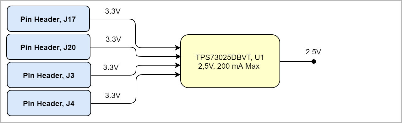 Image Added Image Added |
|
Power-On Sequence
There is no specific power-on sequence. After power on, the module and carrier will be powered on.
| Scroll Title |
|---|
| anchor | Figure_PWR_VMCPS |
|---|
| title | Voltage Monitor CircuitPower Sequency |
|---|
|
| Scroll Ignore |
|---|
| draw.io Diagram |
|---|
| border | false |
|---|
| viewerToolbar | true |
|---|
| |
|---|
| fitWindow | false |
|---|
| diagramDisplayName | |
|---|
| lbox | true |
|---|
| revision | 3 |
|---|
| diagramName | TEBA0714_PWR_PS |
|---|
| simpleViewer | false |
|---|
| width | |
|---|
| links | auto |
|---|
| tbstyle | hidden |
|---|
| diagramWidth | 640 |
|---|
|
|
| Scroll Only |
|---|
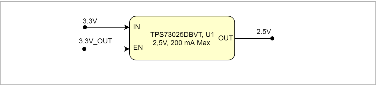 Image Added Image Added | Create DrawIO object here: Attention if you copy from other page, objects are only linked. | | Scroll Only |
|---|
| image link to the generate DrawIO PNG file of this page. This is a workaround until scroll pdf export bug is fixed |
|
Power Rails
| Scroll Title |
|---|
| anchor | Table_PWR_PR |
|---|
| title | Module power rails. |
|---|
|
| Scroll Table Layout |
|---|
| orientation | portrait |
|---|
| sortDirection | ASC |
|---|
| repeatTableHeaders |
|---|
|
| default | style | widths |
|---|
| sortByColumn | 1 |
|---|
| sortEnabled | false |
|---|
| cellHighlighting | true |
|---|
| Power Rail Name | B2B Connector JM1 Pin | B2B Connector JM2 Pin | B2B Connector JM3 Pin | Direction | Notes |
|---|
Bank Voltages
| default |
|---|
| style | |
|---|
| widths | |
|---|
| sortByColumn | 1 |
|---|
| sortEnabled | false |
|---|
| cellHighlighting | true |
|---|
|
| Power Rail Name | B2B , JM1 Pin | B2B JM2 Pin | Pin Header J17 | Pin Header J20 | Pin Header J3 | Pin Header J4 | Direction | Notes |
|---|
| 3.3V | 99,97 | - | 5, 46 | 5, 46 | 5 | 5 | Input |
| | 1.8V | - | 18 | - | - | - | - | Input | Comes from Module | | 3.3V_OUT | 83 | 54 | - | - | - | 6 | Output |
| | VCCIO34 | 61 | - | - | 45 | - | - | Output | Variable voltage level | | V_CFG | 53 | - | - | - | - | - | Input | Variable voltage level |
|
| Scroll Title |
|---|
| anchor | Table_PWR_BV |
|---|
| title | Zynq SoC bank voltages. |
|---|
|
| Scroll Table Layout |
|---|
|
| orientation | portrait |
|---|
| sortDirection | ASC |
|---|
| repeatTableHeaders | default |
|---|
style | widths | | sortByColumn | 1 |
|---|
| sortEnabled | false |
|---|
| cellHighlighting | true |
|---|
Board to Board Connectors
| Page properties |
|---|
|
- This section is optional and only for modules.
- use "include page" macro and link to the general B2B connector page of the module series,For example: 6 x 6 SoM LSHM B2B Connectors
PD: | 6 x 6 SoM LSHM B2B Connectors |
|---|
|
PD: | 6 x 6 SoM LSHM B2B Connectors |
|---|
|
|
? x ? modules use two or three Samtec Micro Tiger Eye ConnectorTEBA0714 carrier use two Samtec Razor Beam LSHM Connectors on the bottom side.
3 x REF-??????? (compatible to ????????), (?? pins, ?? per row)
| Include Page |
|---|
| 4 x 5 SoM LSHM B2B Connectors |
|---|
| 4 x 5 SoM LSHM B2B Connectors |
|---|
|
...
Technical Specifications
Absolute Maximum Ratings
| Scroll Title |
|---|
| anchor | Table_TS_AMR |
|---|
| title | PS absolute maximum ratings |
|---|
|
| Scroll Table Layout |
|---|
| orientation | portrait |
|---|
| sortDirection | ASC |
|---|
| repeatTableHeaders | default |
|---|
| style | |
|---|
| widths | |
|---|
| sortByColumn | 1 |
|---|
| sortEnabled | false |
|---|
| cellHighlighting | true |
|---|
|
| Symbols | Description | Min | Max | Unit |
|---|
|
|---|
| VIN | Input Supply Voltage | -0.3 | 6 |
V | VV | | T_STR | Storage Temperature | -40 | 125 | °C |
V | V | V | V
|
Recommended Operating Conditions
...
| Scroll Title |
|---|
| anchor | Table_TS_ROC |
|---|
| title | Recommended operating conditions. |
|---|
|
| Scroll Table Layout |
|---|
| orientation | portrait |
|---|
| sortDirection | ASC |
|---|
| repeatTableHeaders | default |
|---|
| style | |
|---|
| widths | |
|---|
| sortByColumn | 1 |
|---|
| sortEnabled | false |
|---|
| cellHighlighting | true |
|---|
|
|
| Parameter | Min | Max | Units | Reference Document |
|---|
V | See ???? datasheets. | V | See Xilinx ???? datasheet. | V | See Xilinx ???? datasheet. | V | See Xilinx ???? datasheet. | V | See Xilinx ???? datasheet. | V | See Xilinx ???? datasheet. | V | See Xilinx ???? datasheet. | °C | See Xilinx ???? datasheet. | °C | See Xilinx ???? datasheet. | | Parameter | Min | Max | Units | Reference Document |
|---|
| VIN | 3.135 | 3.465 | V | 3.3V Nominal Power Supply |
| T_OPR | -40 | 85 | °C |
|
Physical Dimensions
- Module size: ?? 46 mm × ?? 75 mm. Please download the assembly diagram for exact numbers.
- Mating height with standard connectors: ? 8 mm.
PCB thickness: ?? 1.64 mm.
| Page properties |
|---|
|
In 'Physical Dimension' section, top and bottom view of module must be inserted, information regarding physical dimensions can be obtained through webpage for product in Shop.Trenz, (Download> Documents> Assembly part) for every SoM. For Example: for Module TE0728, Physical Dimension information can be captured by snipping tools from the link below: https://www.trenz-electronic.de/fileadmin/docs/Trenz_Electronic/Modules_and_Module_Carriers/5.2x7.6/TE0745/REV02/Documents/AD-TE0745-02-30-1I.PDF
|
| Scroll Title |
|---|
| anchor | Figure_TS_PD |
|---|
| title | Physical Dimension |
|---|
|
| Scroll Ignore |
|---|
| draw.io Diagram |
|---|
| border | false |
|---|
| viewerToolbar | true |
|---|
| |
|---|
| fitWindow | false |
|---|
| diagramDisplayName | |
|---|
| lbox | true |
|---|
| revision | 1 |
|---|
| diagramName | TEBA0714 |
|---|
|
|
|
| Scroll Title |
|---|
| anchor | Figure |
|---|
| title | Physical Dimension |
|---|
| simpleViewer | false |
|---|
| width | |
|---|
| links | auto |
|---|
| tbstyle | hidden |
|---|
| diagramWidth | 641 |
|---|
|
| | Scroll Ignore |
|---|
| Create DrawIO object here: Attention if you copy from other page, objects are only linked. |
| Scroll Only |
|---|
| scroll-pdf | true |
|---|
| scroll-office | true |
|---|
| scroll-chm | true |
|---|
| scroll-docbook | true |
|---|
| scroll-eclipsehelp | true |
|---|
| scroll-epub | true |
|---|
| scroll-html | true |
|---|
| true |
|---|
| scroll-html | true |
|---|
| 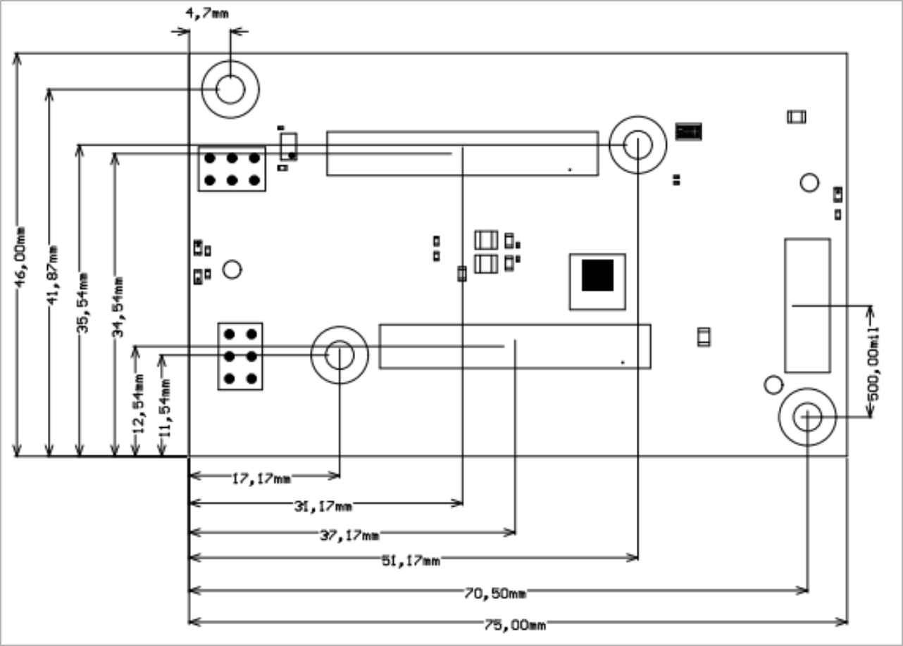 Image Addedimage link to the generate DrawIO PNG file of this page. This is a workaround until scroll pdf export bug is fixed Image Addedimage link to the generate DrawIO PNG file of this page. This is a workaround until scroll pdf export bug is fixed |
|
Currently Offered Variants
| Scroll Title |
|---|
| anchor | Table_VCP_SO |
|---|
| title | Trenz Electronic Shop Overview |
|---|
|
| Scroll Table Layout |
|---|
| orientation | portrait |
|---|
| sortDirection | ASC |
|---|
| repeatTableHeaders | default |
|---|
| style | |
|---|
| widths | |
|---|
| sortByColumn | 1 |
|---|
| sortEnabled | false |
|---|
| cellHighlighting | true |
|---|
|
|
Revision History
Hardware Revision History
| Scroll Title |
|---|
| anchor | Table_RH_HRH |
|---|
| title | Hardware Revision History |
|---|
|
| Scroll Table Layout |
|---|
| orientation | portrait |
|---|
| sortDirection | ASC |
|---|
| repeatTableHeaders | default |
|---|
| style | |
|---|
| widths | |
|---|
| sortByColumn | 1 |
|---|
| sortEnabled | false |
|---|
| cellHighlighting | true |
|---|
|
| Date | Revision | Changes | Documentation Link |
|---|
| 2016-06-15 | 01 | | REV01 |
|
Hardware revision number can be found on the PCB board together with the module model number separated by the dash..
| Scroll Title |
|---|
| anchor | Figure_RV_HRN |
|---|
| title | Board hardware revision number. |
|---|
|
| Scroll Ignore |
|---|
| draw.io Diagram |
|---|
| border | true |
|---|
| viewerToolbar | true |
|---|
| |
|---|
| fitWindow | false |
|---|
| diagramName |
|---|
|
|
|
| Scroll Title |
|---|
anchor |
| title | Board hardware revision number. |
|---|
| simpleViewer | false |
|---|
| width | |
|---|
| diagramWidth | 146 |
|---|
| revision | 1 |
|---|
|
|
| Scroll Only |
|---|
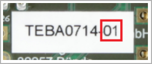 Image Added Image Added |
| Scroll Ignore |
|---|
Create DrawIO object here: Attention if you copy from other page, objects are only linked. |
| Scroll Only |
|---|
| image link to the generate DrawIO PNG file of this page. This is a workaround until scroll pdf export bug is fixed |
|
Document Change History
| Page properties |
|---|
|
- Note this list must be only updated, if the document is online on public doc!
- It's semi automatically, so do following
- Add new row below first
- Copy "Page Information Macro(date)" Macro-Preview, Metadata Version number, Author Name and description to the empty row. Important Revision number must be the same as the Wiki document revision number Update Metadata = "Page Information Macro (current-version)" Preview+1 and add Author and change description. --> this point is will be deleted on newer pdf export template
- Metadata is only used of compatibility of older exports
|
...
| Scroll Title |
|---|
| anchor | Table_RH_DCH |
|---|
| title | Document change history. |
|---|
|
| Scroll Table Layout |
|---|
| orientation | portrait |
|---|
| sortDirection | ASC |
|---|
| repeatTableHeaders | default |
|---|
| style | |
|---|
| widths | |
|---|
| sortByColumn | 1 |
|---|
| sortEnabled | false |
|---|
| cellHighlighting | true |
|---|
|
| Date | Revision | Contributor | Description |
|---|
| Page info |
|---|
| infoType | Modified date |
|---|
| dateFormat | yyyy-MM-dd |
|---|
| type | Flat |
|---|
|
| | Page info |
|---|
| infoType | Current version |
|---|
| prefix | v. |
|---|
| type | Flat |
|---|
| showVersions | false |
|---|
|
| | Page info |
|---|
| infoType | Modified by |
|---|
| type | Flat |
|---|
| showVersions | false |
|---|
|
| - change listInitial Release
| | -- | all | | Page info |
|---|
| infoType | Modified users |
|---|
| type | Flat |
|---|
| showVersions | false |
|---|
|
| |
|
Disclaimer
| Include Page |
|---|
| IN:Legal Notices |
|---|
| IN:Legal Notices |
|---|
|
...