Page History
...
| HTML |
|---|
<!--
Link to the base folder of the module (remove de/ or en/ from the URL): for example:
https://shop.trenz-electronic.de/Download/?path=Trenz_Electronic/Modules_and_Module_Carriers/4x5/4x5_Carriers/TE0703/
--> |
| Scroll Ignore |
|---|
| Scroll pdf ignore | |
|---|---|
Table of Contents
|
Overview
The Trenz Electronic TE0782 TE0783 is a high-performance, industrial-grade SoM (System on Module) with industrial temperature range based on Xilinx Zynq-7000 SoC (XC7Z035, XC7Z045 or XC7Z100).
...
| HTML |
|---|
<!-- Use short link the Wiki Ressource page: for example: http://trenz.org/te0782TE0783-info List of available short links: https://wiki.trenz-electronic.de/display/CON/Redirects --> |
...
| Scroll Only (inline) |
|---|
Refer to http://trenz.org/te0782te0783-info for the current online version of this manual and other available documentation. |
Key Features
- Xilinx Zynq-7000 XC7Z035, XC7Z045 or XC7Z100 -7000 XC7Z045-2FFG900I SoC
- Rugged for shock and high vibration
- Large number of configurable I/Os are provided via rugged high-speed stacking strips
- Dual ARM Cortex-A9 MPCore
- 1 GByte RAM (32-Bit 32bit wide DDR3) connected to PS
- 2 GByte RAM (64bit wide DDR3) connected to PL
- 32 MByte QSPI Flash memory
- 2 x Hi-Speed USB2 ULPI transceiver PHY
- 2 x Gigabit (10/100/1000 Mbps) Ethernet transceiver PHY
- 4 GByte eMMC (optional up to 64 GByte)
- Lattice MachXO2 HC 4000 System Controller CPLD
- 40 GPIO's available to user on B2B connector
- 2 x MAC-address EEPROMsEEPROM
- Serial user EEPROMOptional 2x 64 MByte HyperFLASH or 2x 8 MByte HyperRAM (max 2x 32 MByte HyperRAM)
- Temperature compensated RTC (real-time clock)
- Si5338A programmable quad PLL clock generator for GTX transceiver clocks
- Plug-on module with 3 x 160-pin high-speed strips
- 16 GTX high-performance transceiver
- 2x 4x GT transceiver clock inputs
- 254 166 FPGA I/O's (125 83 LVDS pairs)
- On-board high-efficiency switch-mode DC-DC converters
- System management
- eFUSE bit-stream encryption
- AES bit-stream encryption
- Evenly-spread supply pins for good signal integrity
- User LED
...
| Scroll Title | ||||||||||||||||||||||||||||||||
|---|---|---|---|---|---|---|---|---|---|---|---|---|---|---|---|---|---|---|---|---|---|---|---|---|---|---|---|---|---|---|---|---|
| ||||||||||||||||||||||||||||||||
|
Main Components
| Scroll Title | |||||||||||||||||||||||||||||||||
|---|---|---|---|---|---|---|---|---|---|---|---|---|---|---|---|---|---|---|---|---|---|---|---|---|---|---|---|---|---|---|---|---|---|
| |||||||||||||||||||||||||||||||||
|
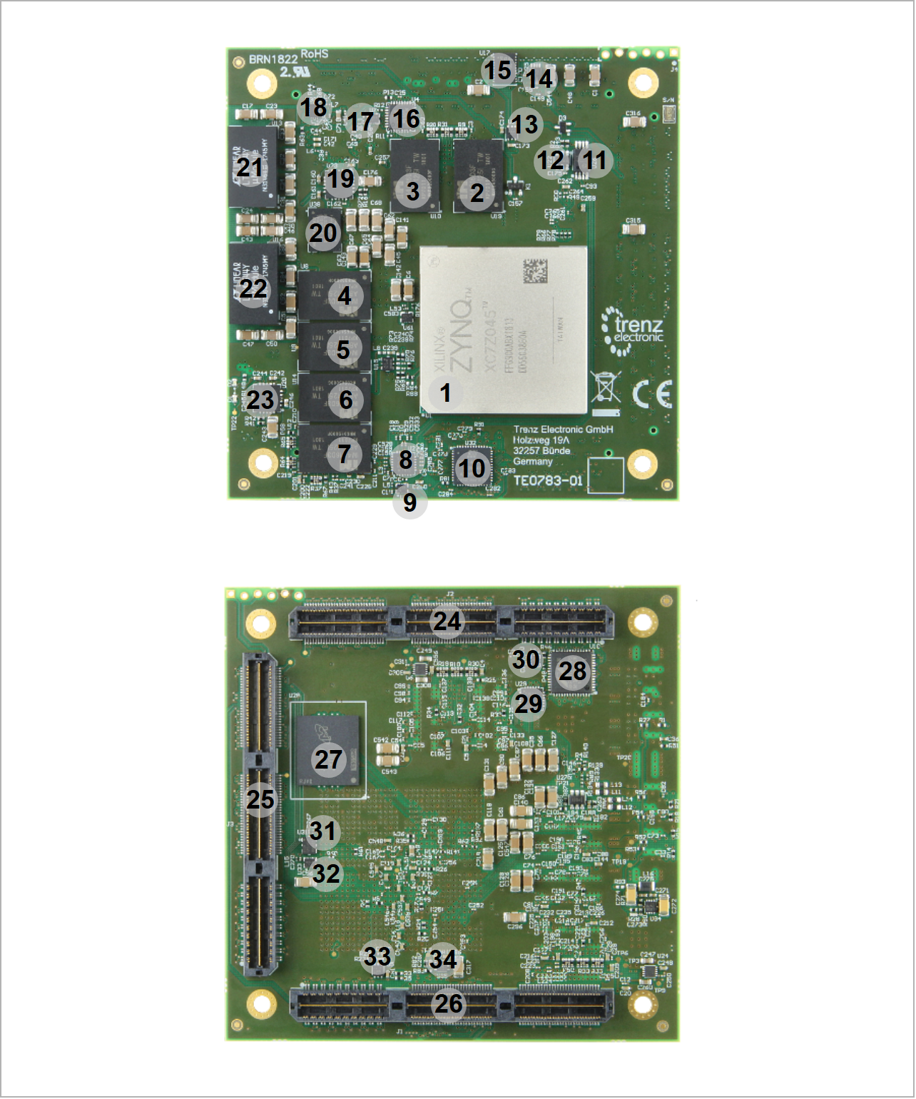
- Xilinx Zynq-7000 SoC, U1
- 4Gbit DDR3L SDRAM, U19
- 4Gbit DDR3L SDRAM, U10
- 4Gbit DDR3L SDRAM, U8
- 4Gbit DDR3L SDRAM, U9
- 4Gbit DDR3L SDRAM, U14
- 4Gbit DDR3L SDRAM, U12
- SI5338A programmable quad PLL clock generator, U2
- SiTime SiT8008 25.000000 MHz oscillator, U3
- Lattice Semiconductor MachXO2 4000HC CPLD, U32
- Xilinx Zynq UltraScale+ MPSoC, U1
- Lattice Semiconductor MachXO2 1200HC CPLD, U14
- 4Gbit DDR3L SDRAM, U19
- 4Gbit DDR3L SDRAM, U10
- I²C voltage translator, U25
- Intersil ISL12020MIRZ Real Time Clock, U17
- Microchip USB3320C USB PHY transceiver, U4
- Microchip USB3320C USB PHY transceiver, U8
- SiTime SiT8008 52.000000 MHz oscillator, U7
- 32 MByte QSPI Flash memory, U38
- SiTime SiT8008 33.333333 MHz oscillator, U61
- SI5338A programmable quad PLL clock generator, U2
- SiTime SiT8008 25.000000 MHz oscillator, U3
- TPS74801 LDO @1.5V, U23
- LT quad 4A PowerSoC DC-DC converter (@1.0V), U13
- LT quad 4A PowerSoC DC-DC converter (@3.3V, @1,8V, @1.2V_MGT, @1.0V_MGT), U16
- Samtec ASP-122952-01 160-pin stacking strip (2 rows a 80 positions), J2
- Samtec ASP-122952-01 160-pin stacking strip (2 rows a 80 positions), J3
- Samtec ASP-122952-01 160-pin stacking strip (2 rows a 80 positions), J1
- Marvell Alaska 88E1512 Gigabit Ethernet PHY, 20
- Marvell Alaska 88E1512 Gigabit Ethernet PHY, U18
- Micron Technology 4 GByte eMMC, U15
- Microchip 128Kbit I²C EEPROM, U26
- Microchip 2Kbit I²C MAC EEPROM, U24
- Microchip 2Kbit I²C MAC EEPROM, U22
- TPS51206 DDR reference voltage and termination regulator, U6
- TPS799 LDO @1.8V_MGT, U5
- U22
- TPS780180300 LDO @1.8V backup battery voltage, U21
- TCA9406DCUR I²C voltage level shifter, U25
- Intersil ISL12020MIRZ Real Time Clock, U17
- Microchip USB3320C USB PHY transceiver, U4
- SiTime SiT8008 52SiTime SiT8008 25.000000 MHz oscillator, U11
Initial Delivery State
...
24AA025E48 EEPROM's
...
User content not programmed
...
SPI Flash OTP Area
...
Empty, not programmed
...
Except serial number programmed by flash vendor
...
SPI Flash Quad Enable bit
...
Programmed
...
SPI Flash main array
...
demo design
...
eFUSE USER
...
Not programmed
...
-
...
eFUSE Security
...
Not programmed
...
Table 1: Initial delivery state of programmable devices on the module
Boot Process
4 of the 7 boot mode strapping pins (MIO2 ... MIO8) of the Xilinx Zynq-7000 SoC device are hardware programmed on the board, 3 of them are set be the SC CPLD firmware. They are evaluated by the Zynq device soon after the 'PS_POR' signal is deasserted to begin the boot process (see section "Boot Mode Pin Settings" of Xilinx manual UG585).
The TE0782 board is programmed in the SC CPLD firmware to boot initially from the on-board QSPI Flash memory U38. See section Bootmode in the TE0782 SC CPLD reference Wiki page.
The JTAG interface of the module is provided for storing the data to the QSPI Flash memory through the Zynq-7000 device.
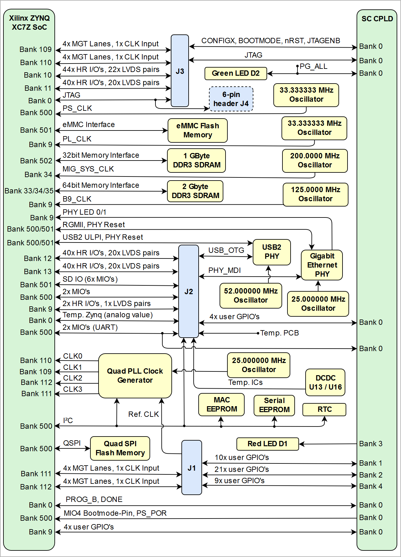
Signals, Interfaces and Pins
Board to Board (B2B) I/Os
Zynq-7000 SoC's I/O banks signals connected to the B2B connectors:
...
B2B Connector
...
I/O Signal Count
...
10
...
HR
...
J3
...
44
...
User
...
11
...
HR
...
J3
...
40
...
User
...
HR
...
J2
...
40
...
User
...
13
...
HR
...
J2
...
40
...
User
...
33
...
HP
...
J1
...
48
...
User
...
Table 2: General overview of board to board I/O signals
For detailed information about the pin-out, please refer to the Pin-out table.
MGT Lanes
The Xilinx Zynq-7000 SoC used on the TE0782 module has 16 MGT transceiver lanes. All of them are wired directly to B2B connectors J1 and J3. MGT (Multi Gigabit Transceiver) lane consists of one transmit and one receive (TX/RX) differential pairs, four signals total per one MGT lane with data transmission rates up to 12.5Gb/s per lane (Xilinx GTX transceiver). Following table lists lane number, FPGA bank number, transceiver type, signal schematic name, board-to-board pin connection and FPGA pins connection:
...
- MGT_RX0_P
- MGT_RX0_N
- MGT_TX0_P
- MGT_TX0_N
...
- J3-32
- J3-30
- J3-31
- J3-29
...
- MGTXRXP0_109
- MGTXRXN0_109
- MGTXTXP0_109
- MGTXTXN0_109
...
- MGT_RX1_P
- MGT_RX1_N
- MGT_TX1_P
- MGT_TX1_N
...
- J3-28
- J3-26
- J3-27
- J3-25
...
- MGTXRXP1_109
- MGTXRXN1_109
- MGTXTXP1_109
- MGTXTXN1_109
...
- MGT_RX2_P
- MGT_RX2_N
- MGT_TX2_P
- MGT_TX2_N
...
- J3-24
- J3-22
- J3-23
- J3-21
...
- MGTXRXP2_109
- MGTXRXN2_109
- MGTXTXP2_109
- MGTXTXN2_109
...
- MGT_RX3_P
- MGT_RX3_N
- MGT_TX3_P
- MGT_TX3_N
...
- J3-20
- J3-18
- J3-19
- J3-17
...
- MGTXRXP3_109
- MGTXRXN3_109
- MGTXTXP3_109
- MGTXTXN3_109
...
- MGT_RX4_P
- MGT_RX4_N
- MGT_TX4_P
- MGT_TX4_N
...
- J3-16
- J3-14
- J3-15
- J3-13
...
- MGTXRXP0_110
- MGTXRXN0_110
- MGTXTXP0_110
- MGTXTXN0_110
...
- MGT_RX5_P
- MGT_RX5_N
- MGT_TX5_P
- MGT_TX5_N
...
- J3-12
- J3-10
- J3-11
- J3-9
...
- MGTXRXP1_110
- MGTXRXN1_110
- MGTXTXP1_110
- MGTXTXN1_110
...
- MGT_RX6_P
- MGT_RX6_N
- MGT_TX6_P
- MGT_TX6_N
...
- J3-8
- J3-6
- J3-7
- J3-5
...
- MGTXRXP2_110
- MGTXRXN2_110
- MGTXTXP2_110
- MGTXTXN2_110
...
- MGT_RX7_P
- MGT_RX7_N
- MGT_TX7_P
- MGT_TX7_N
...
- J3-4
- J3-2
- J3-3
- J3-1
...
- MGTXRXP3_110
- MGTXRXN3_110
- MGTXTXP3_110
- MGTXTXN3_110
...
- MGT_RX8_P
- MGT_RX8_N
- MGT_TX8_P
- MGT_TX8_N
...
- J3-1
- J3-3
- J3-2
- J3-4
...
- MGTXRXP0_111
- MGTXRXN0_111
- MGTXTXP0_111
- MGTXTXN0_111
...
- MGT_RX9_P
- MGT_RX9_N
- MGT_TX9_P
- MGT_TX9_N
...
- J3-5
- J3-7
- J3-6
- J3-8
...
- MGTXRXP1_111
- MGTXRXN1_111
- MGTXTXP1_111
- MGTXTXN1_111
...
- MGT_RX10_P
- MGT_RX10_N
- MGT_TX10_P
- MGT_TX10_N
...
- J3-9
- J3-11
- J3-10
- J3-12
...
- MGTXRXP2_111
- MGTXRXN2_111
- MGTXTXP2_111
- MGTXTXN2_111
...
- MGT_RX11_P
- MGT_RX11_N
- MGT_TX11_P
- MGT_TX11_N
...
- J3-13
- J3-15
- J3-14
- J3-16
...
- MGTXRXP3_111
- MGTXRXN3_111
- MGTXTXP3_111
- MGTXTXN3_111
...
- MGT_RX12_P
- MGT_RX12_N
- MGT_TX12_P
- MGT_TX12_N
...
- J3-17
- J3-19
- J3-18
- J3-20
...
- MGTXRXP0_112
- MGTXRXN0_112
- MGTXTXP0_112
- MGTXTXN0_112
...
- MGT_RX13_P
- MGT_RX13_N
- MGT_TX13_P
- MGT_TX13_N
...
- J3-21
- J3-23
- J3-22
- J3-24
...
- MGTXRXP1_112
- MGTXRXN1_112
- MGTXTXP1_112
- MGTXTXN1_112
...
- MGT_RX14_P
- MGT_RX14_N
- MGT_TX14_P
- MGT_TX14_N
...
- J3-25
- J3-27
- J3-26
- J3-28
...
- MGTXRXP2_112
- MGTXRXN2_112
- MGTXTXP2_112
- MGTXTXN2_112
...
- MGT_RX15_P
- MGT_RX15_N
- MGT_TX15_P
- MGT_TX15_N
...
- J3-29
- J3-31
- J3-30
- J3-32
...
- MGTXRXP3_112
- MGTXRXN3_112
- MGTXTXP3_112
- MGTXTXN3_112
Table 3: MGT lanes
There are 2 clock sources for the GTX transceivers. MGT_CLK1 and MGT_CLK4 are connected directly to B2B connector J3 and J1, so the clock can be provided by the carrier board. Clocks MGT_CLK0, MGT_CLK3, MGT_CLK5 and MGT_CLK6 are provided by the on-board clock generator (U2). As there are no capacitive coupling of the data and clock lines that are connected to the connectors, these may be required on the user’s PCB depending on the application.
...
Table 4: MGT reference clock sources
JTAG Interface
JTAG access to the Xilinx Zynq-7000 is provided through B2B connector J3.
...
JTAG Signal
...
B2B Connector Pin
...
Table 5: Zynq JTAG interface signals
JTAG access to the LCMXO2-1200HC System Controller CPLD U14 is provided through B2B connector J3.
...
JTAG Signal
...
B2B Connector Pin
...
Pin J3-136 'JTAGENB' of B2B connector J3 is used to access the JTAG interface of the SC CPLD. Set high to program the System Controller CPLD via JTAG interaface.
System Controller CPLD I/O Pins
Special purpose pins are connected to System Controller CPLD and have following default configuration:
...
Bootmode Pins
currently configured in SC CPLD firmare to boot from QSPI Flash
...
reset USB2 PHYs
U4 and U8
...
Table 7: System Controller CPLD special purpose pins.
See also TE0782 CPLD reference Wiki page.
Default PS MIO Mapping
...
Table 8: Zynq PS MIO mapping
Gigabit Ethernet
...
- U7
- 74AVCH4T245 voltage level tranlator, U30
- TPS74801RGW LDO @1.5V, U23
- 32 MByte QSPI Flash memory, U38
- LT quad 4A PowerSoC DC-DC converter (@1.0V), U13
- LT quad 4A PowerSoC DC-DC converter (@3.3V, @1,8V, @1.2V_MGT, @1.0V_MGT), U16
- TPS74801RGW LDO @1.5V_PL, U20
- Samtec ASP-122952-01 160-pin stacking strip (2 rows a 80 positions), J2
- Samtec ASP-122952-01 160-pin stacking strip (2 rows a 80 positions), J3
- Samtec ASP-122952-01 160-pin stacking strip (2 rows a 80 positions), J1
- Micron Technology 4 GByte eMMC, U28
- Marvell Alaska 88E1512 Gigabit Ethernet PHY, U18
- Texas Instruments TXS02612RTWR SDIO Port Expander, U29
- SiTime SiT8008 25.000000 MHz oscillator, U11
- DSC1123CI2 Low-Jitter Precision LVDS Oscillator, U31
- SiTime SiT8008 33.333333 MHz oscillator, U33
- TPS799 LDO @1.8V_MGT, U5
- TPS799 LDO @VCCAUX_IO (1.8V), U35
Initial Delivery State
| Storage device name | Content | Notes |
|---|---|---|
| 24LC128-I/ST EEPROM | not programmed | User content |
24AA025E48 EEPROM | User content not programmed | Valid MAC Address from manufacturer |
| Si5338A OTP Area | not programmed | - |
| eMMC Flash Memory | Empty, not programmed | Except serial number programmed by flash vendor |
SPI Flash OTP Area | Empty, not programmed | Except serial number programmed by flash vendor |
SPI Flash Quad Enable bit | Programmed | - |
SPI Flash main array | demo design | - |
eFUSE USER | Not programmed | - |
eFUSE Security | Not programmed | - |
Table 1: Initial delivery state of programmable devices on the module
Boot Process
6 of the 7 boot mode strapping pins (MIO2 ... MIO8) of the Xilinx Zynq-7000 SoC device are hardware programmed on the board, 1 of them is set by the SC CPLD firmware. The boot strapping pins are evaluated by the Zynq device soon after the 'PS_POR' signal is deasserted to begin the boot process (see section "Boot Mode Pin Settings" of Xilinx manual UG585).
The TE0783 boot mode is selected by the pin 'CPLD_GPIO3' of the SC CPLD, which is connected to B2B pin J2-16 to either boot from the on-board QSPI Flash memory U38 or SD IO interface. See section Bootmode in the TE0783 SC CPLD reference Wiki page.
The JTAG interface of the module is provided for storing the data to the QSPI Flash memory through the Zynq-7000 device.
Signals, Interfaces and Pins
Board to Board (B2B) I/Os
Zynq-7000 SoC's I/O banks signals connected to the B2B connectors:
| Bank | Type | B2B Connector | I/O Signal Count | Differential | Voltage | Notes |
|---|---|---|---|---|---|---|
| 9 | HR | J2 | 2 | 1 | 3.3V | fixed bank voltage to 3.3V |
10 | HR | J3 | 44 | 22 | User | Max voltage 3.3V |
11 | HR | J3 | 40 | 20 | User | Max voltage 3.3V |
| 12 | HR | J2 | 40 | 20 | User | Max voltage 3.3V |
13 | HR | J2 | 40 | 20 | User | Max voltage 3.3V |
Table 2: General overview of board to board I/O signals
For detailed information about the pin-out, please refer to the Pin-out table.
MGT Lanes
The Xilinx Zynq-7000 SoC used on the TE0783 module has 16 MGT transceiver lanes. All of them are wired directly to B2B connectors J1 and J3. MGT (Multi Gigabit Transceiver) lane consists of one transmit and one receive (TX/RX) differential pairs, four signals total per one MGT lane with data transmission rates up to 12.5Gb/s per lane (Xilinx GTX transceiver). Following table lists lane number, FPGA bank number, transceiver type, signal schematic name, board-to-board pin connection and FPGA pins connection:
| Bank | Type | Lane | Signal Name | B2B Pin | FPGA Pin |
|---|---|---|---|---|---|
| 109 | GTX | 0 |
|
|
|
| 1 |
|
|
| ||
| 2 |
|
|
| ||
| 3 |
|
|
| ||
| 110 | GTX | 0 |
|
|
|
| 1 |
|
|
| ||
| 2 |
|
|
| ||
| 3 |
|
|
| ||
| 111 | GTX | 0 |
|
|
|
| 1 |
|
|
| ||
| 2 |
|
|
| ||
| 3 |
|
|
| ||
| 112 | GTX | 0 |
|
|
|
| 1 |
|
|
| ||
| 2 |
|
|
| ||
| 3 |
|
|
|
Table 3: MGT lanes
There are 2 clock sources for the GTX transceivers. MGT_CLK1, MGT_CLK2, MGT_CLK4 and MGT_CLK7 are connected directly to B2B connector J3 and J1, so the clock can be provided by the carrier board. Clocks MGT_CLK0, MGT_CLK3, MGT_CLK5 and MGT_CLK6 are provided by the on-board clock generator (U2). As there are no capacitive coupling of the data and clock lines that are connected to the connectors, these may be required on the user’s PCB depending on the application.
| Bank | Type | Clock signal | Source | FPGA Pin | Notes |
|---|---|---|---|---|---|
| 109 | GTX | MGT_CLK3_P | U2, CLK3A | MGTREFCLK1P_109, AF10 | Supplied by on-board Si5338A |
| MGT_CLK3_N | U2, CLK3B | MGTREFCLK1N_109, AF9 | |||
| MGT_CLK2_P | J3-38 | MGTREFCLK0P_109, AD10 | Supplied by B2B connector J3 | ||
| MGT_CLK2_N | J3-40 | MGTREFCLK0N_109, AD9 | |||
| 110 | GTX | MGT_CLK0_P | U2, CLK2A | MGTREFCLK0P_110, AA8 | Supplied by on-board Si5338A |
| MGT_CLK0_N | U2, CLK2B | MGTREFCLK0N_110, AA7 | |||
| MGT_CLK1_N | J3-39 | MGTREFCLK1P_110, AC8 | Supplied by B2B connector J3 | ||
| MGT_CLK1_P | J3-37 | MGTREFCLK1N_110, AA7 | |||
| 111 | GTX | MGT_CLK4_N | J1-40 | MGTREFCLK0P_111, U8 | Supplied by B2B connector J1 |
| MGT_CLK4_P | J1-38 | MGTREFCLK0N_111, U7 | |||
| MGT_CLK5_P | U2, CLK1A | MGTREFCLK1P_111, W8 | Supplied by on-board Si5338A | ||
| MGT_CLK5_N | U2, CLK1B | MGTREFCLK1N_111, W7 | |||
| 112 | GTX | MGT_CLK6_P | U2, CLK0A | MGTREFCLK0P_112, N8 | Supplied by on-board Si5338A |
| MGT_CLK6_N | U2, CLK0B | MGTREFCLK0N_112, N7 | |||
| MGT_CLK7_P | J1-37 | MGTREFCLK1P_112, R8 | Supplied by B2B connector J1 | ||
| MGT_CLK7_N | J1-39 | MGTREFCLK1N_112, R7 |
Table 4: MGT reference clock sources
JTAG Interface
JTAG access to the Xilinx Zynq-7000 is provided through B2B connector J3.
JTAG Signal | B2B Connector Pin |
|---|---|
| TMS | J3-142 |
| TDI | J3-147 |
| TDO | J3-148 |
| TCK | J3-141 |
Table 5: Zynq JTAG interface signals
JTAG access to the LCMXO2-1200HC System Controller CPLD U14 is provided through B2B connector J3.
JTAG Signal | B2B Connector Pin |
|---|---|
| M_TMS | J3-82 |
| M_TDI | J3-87 |
| M_TDO | J3-88 |
| M_TCK | J3-81 |
Table 6: System Controller CPLD JTAG interface signals
Pin J3-136 'JTAGENB' of B2B connector J3 is used to access the JTAG interface of the SC CPLD. Set high to program the System Controller CPLD via JTAG interaface.
System Controller CPLD I/O Pins
Special purpose pins are connected to System Controller CPLD (U32) and have following default configuration:
| Pin Name | Direction | Function | Default Configuration |
|---|---|---|---|
| EXT_IO1 ... EXT_IO40 | in / out | user GPIO on B2B | see current CPLD firmware |
| BOOTMODE | in | in | signal forwarded to MIO9 and currently used as UART RX line |
| CONFIGX | in | out | signal forwarded to MIO8 and currently used as UART TX line |
| NRST_IN | in | nRESET input | external Board Reset |
| M_TDO | out | CPLD JTAG interface | - |
| M_TDI | in | ||
| M_TCK | in | ||
| M_TMS | in | ||
| JTAGENB | in | enable JTAG | pull high for programming SC CPLD firmware |
| ETH1_RESET | out | reset GbE PHY U18 | see current SC CPLD firmware |
| OTG-RST | out | reset USB2 PHYs U4 and U8 | see current SC CPLD firmware |
| DONE | in | Zynq control signal | PL configuration completed |
| PROG_B | out | PL configuration reset signal | |
| PS_POR | out | PS power-on reset | |
| BM2/MIO4 | out | Bootmode Pin: SD or QSPI | |
| MIO14 | in | user MIO pins | currently used as UART interface |
| MIO15 | out | ||
| LED2 | out | Red LED D1 status signal | see current CPLD firmware |
| CPLD_GPIO0 ... CPLD_GPIO3 | in / out | CPLD_GPIO3 used for Boot Mode | see current CPLD firmware |
| FPGA_CPLD1 ... FPGA_CPLD4 | in /out | user GPIO to FPGA bank 9 | see current SC CPLD firmware |
| EN_1V | out | Power control | enable signal DCDC U13 '1V' |
| PG_ALL | in | power good signal all voltages powered up properly → Green LED D2 lights up. |
Table 7: System Controller CPLD special purpose pins.
See also TE0783 CPLD reference Wiki page.
Default PS MIO Mapping
| MIO | Function | Connected to |
|---|---|---|
| 0 | USB2 PHY Reset | voltage level translator U30 → USB2 PHY U4 |
| 1 | QSPI0 | SPI Flash-CS |
| 2 | QSPI0 | SPI Flash-DQ0 |
| 3 | QSPI0 | SPI Flash-DQ1 |
| 4 | QSPI0 | SPI Flash-DQ2 |
| 5 | QSPI0 | SPI Flash-DQ3 |
| 6 | QSPI0 | SPI Flash-SCK |
| 7 | GbE PHY Reset | voltage level translator U30 → GbE PHY U18 |
| 8 | not used | 3.3V pull-up for bootmode pin strapping |
| 9 | not connected | - |
| 10 | SCL | I²C clock line |
| 11 | SDA | I²C data line |
| 12 | - | availabe on B2B pin J-22 |
| 13 | - | availabe on B2B pin J-26 |
| 14 | UART RX | input, muxed to B2B by the SC CPLD |
| 15 | UART TX | output, muxed to B2B by the SC CPLD |
| 16..27 | ETH0 | Ethernet RGMII PHY |
| 28..39 | USB0 | USB0 ULPI PHY |
| 40...45 | SD IO | available on B2B connector J2 with 3.3V VCCIO |
| 46...51 | eMMC | connected to on board eMMC Flash memory U28 |
| 52 | ETH0 MDC | - |
| 53 | ETH0 MDIO | - |
Table 8: Zynq PS MIO mapping
Gigabit Ethernet
The TE0783 is equipped with one Marvell Alaska 88E1512 Gigabit Ethernet PHYs (U18). The transceiver PHY is connected to the Zynq PS Ethernet GEM0. The I/O Voltage is fixed at 1.8V for HSTL signaling. The reference clock input of the PHYs is supplied from an on board 25MHz oscillator (U11).
GbE PHY connection:
| PHY PIN | Zynq PS / PL | Notes |
|---|---|---|
| MDC/MDIO | MIO52, MIO53 | - |
| LED0 | Bank 9, Pin AC18 | - |
| LED1 | Bank 9, Pin AC19 | - |
| Interrupt | - | not connected |
| CLK125 | - | 125 MHz clock output not connected |
| CONFIG |
ETH1 PHY connection:
...
Table 9: General overview of the Gigabit Ethernet1 PHY signals
ETH2 PHY connection:
| - | When pin connected to GND, PHY Address is strapped to 0x00 by default | |
| RESETn |
| MIO7 | ETH1_RESET33 (MIO7) → voltage level translator U30 → ETH1_RESET |
| RGMII | MIO16..MIO27 |
| - | |
| MDI |
| - | on B2B J2 connector |
Table 109: General overview of the Gigabit Ethernet2 Ethernet1 PHY signals
USB Interface
The TE0782 TE0783 is equipped with two one USB PHY 's USB3320 from Microchip (U4 (USB0) and U8 (USB1)). The ULPI interface of USB0 the USB PHY is connected to the Zynq PS USB0, ULPI interface of USB1 to Zynq PS USB1. The I/O Voltage is fixed at 1.8V.
The reference clock input of both the PHY 's is supplied from an on board 52MHz oscillator (U7).
USB0 USB2 PHY connection:
| PHY Pin | Zynq PS / PL |
|---|
| B2B Connector J2 | Notes | |
|---|---|---|
| ULPI | MIO28..39 |
| - | Zynq USB0 MIO pins are connected to the PHY | |
| REFCLK |
| - | - | 52MHz from on board oscillator (U7) | |
| REFSEL[0..2] |
| - | - | 000 GND, select 52MHz reference Clock | |
| RESETB | MIO0 |
| - | OTG |
| -RESET33 → voltage level translator U30 → OTG-RESET | |
| CLKOUT | MIO36 |
| - | Connected to 1.8V selects reference clock operation mode | |
| DP,DM |
| - | USB1_D_P, USB1_D_N | USB Data lines | |
| CPEN | - |
| VBUS1_V_EN | External USB power switch active high enable signal |
| VBUS | - |
| USB1_VBUS | Connect to USB VBUS via a series resistor. Check reference schematic. |
| ID | - |
| OTG1_ID | For an A-Device connect to ground, for a B-Device left floating |
Table 1110: General overview of the Gigabit Ethernet2 PHY signals
USB1 PHY connection:
...
Table 12: General overview of the Gigabit Ethernet2 PHY signals
I2C Interface
The on-board I2C components are connected to bank 35 pins L15 (I2C_SDA) and L14 (I2C_SCL).
I2C addresses for on-board components:
...
Table 13: Address table of the I2C bus slave devices
Pin Definitions
Pins with names ending with _VRN and _VRP are connected to Zynq PL HP bank special purpose pins VRN/VRP and can be routed to DCI calibration resistors on the baseboard. Otherwise they are usable as general purpose I/Os.
Bank 35 has 100 ohm DCI calibration resistors installed, it is also possible to "borrow" the DCI calibration from bank 35 for banks 34 and 33. For more detailed information about the DCI check Xilinx documentation.
On-board Peripherals
System Controller CPLD
The System Controller CPLD (U14) is provided by Lattice Semiconductor LCMXO2-1200HC (MachXO2 product family). It is the central system management unit with module specific firmware installed to monitor and control various signals of the FPGA, on-board peripherals, I/O interfaces and module as a whole.
See also TE0782 CPLD reference Wiki page.
eMMC Flash Memory
eMMC Flash memory device (U15) is connected to the Zynq PS MIO bank 500 pins MIO10..MIO15. eMMC chips MTFC4GMVEA-4M IT (Flash NAND-IC 2x 16 Gbit) is used with 4 GByte of memory density.
DDR4 Memory
By default TE0782-02 module has two 16-bit wide IM (Intelligent Memory) IM4G16D3FABG-125I DDR3L SDRAM (DDR3-1600 Speedgrade) chips arranged into 32-bit wide memory bus providing total of 1 GBytes of on-board RAM.
Quad SPI Flash Memory
Two quad SPI compatible serial bus flash memory for FPGA configuration file storage is provided by Spansion S25FL256SAGBHI20 with 256 Mbit (32 MByte) memory density. After configuration completes the remaining free memory can be used for application data storage. All four SPI data lines are connected to the FPGA allowing x1, x2 or x4 data bus widths to be used. The maximum data transfer rate depends on the bus width and clock frequency.
Gigabit Ethernet PHYs
On-board Gigabit Ethernet PHYs (U18, U20) are provided by Marvell Alaska 88E1512. The Ethernet PHYs' RGMII interfaces are connected to the Zynq's PS MIO bank 501 and to PL bank 9. I/O voltage is fixed at 1.8V for HSTL signaling. The reference clock input of both PHYs is supplied from an on-board 25.000000 MHz oscillator (U11).
High-speed USB ULPI PHYs
Hi-speed USB ULPI PHYs (U4. U8) are provided with USB3320 from Microchip. The ULPI interfaces are connected to the Zynq PS USB0 and USB1 via MIO28..51, bank 501 (see also section USB interface). The I/O voltage is fixed at 1.8V and PHY reference clock input is supplied from the on-board 52.000000 MHz oscillator (U7).
MAC Address EEPROMs
Two Microchip 24AA025E48 serial EEPROMs (U22, U24) contain globally unique 48-bit node address, which are compatible with EUI-48(TM) specification. The devices are organized as two blocks of 128 x 8 Kbit memory. One of the blocks stores the 48-bit node address and is write protected, the other block is available for application use. The MAC address EEPROMS areaccessible over I2C bus (see also section I²C interface).
Configuration EEPROM
The TE0782 board contains one EEPROM (U26) for configuration and general user purposes. The EEPROMs is provided by Microchip 24LC128-I/ST with 128 KBit memory density, the EEPROM is areaccessible over I2C bus (see also section I²C interface).
Programmable Clock Generator
There is a Silicon Labs I2C programmable clock generator Si5338A (U2) chip on-board. It's output frequencies can be programmed using the I2C bus address 0x70 or 0x71. Default address is 0x70, IN4/I2C_LSB pin must be set to high for address 0x71.
A 25.000000 MHz oscillator (U3) is connected to the pin IN3 and is used to generate the output clocks. The output voltage of the oscillator is provided by the 1.8V power rail, thus making output frequency available as soon as 1.8V is present. All 4 of the Si5338 clock outputs are connected to the MGT banks of the Zynq device. It is possible to use the clocks connected to the GTR bank in the user's logic design. This is achieved by instantiating a IBUFDSGTE buffer in the design.
Once running, the frequency and other parameters can be changed by programming the device using the I2C bus connected between the FPGA (master) and clock generator (slave). For this, proper I2C bus logic has to be implemented in FPGA.
...
External clock signal supply from B2B connector J3, pins J3-38 / J3-40
...
IN3
...
25.000000 MHz
...
Fixed input clock signal from reference clock generator SiT8008BI-73-18S-25.000000E (U3)
...
IN5
...
-
...
Not connected
...
IN6
...
-
...
-
...
reference clock 0 of Bank 112 GTX
...
CLK1 A/B
...
reference clock 1 of Bank 111 GTX
...
CLK2 A/B
...
-
...
reference clock 0 of Bank 110 GTX
...
Table 14: General overview of the on-board quad clock generator I/O signals
Oscillators
The module has following reference clock signals provided by on-board oscillators and external source from carrier board:
...
Table 15: Reference clock signals
On-board LEDs
...
Table 16: On-board LEDs
Power and Power-on Sequence
Power Supply
Power supply with minimum current capability of 3A for system startup is recommended.
Power Consumption
...
Table 17: Power consumption
* TBD - To Be Determined soon with reference design setup.
Single 3.3V power supply with minimum current capability of 4A for system startup is recommended.
For the lowest power consumption and highest efficiency of the on-board DC-DC regulators it is recommended to power the module from one single 3.3V supply. All input power supplies should have a nominal value of 3.3V. Although the input power supplies can be powered up in any order, it is recommended to power them up simultaneously.
| Warning |
|---|
| To avoid any damage to the module, check for stabilized on-board voltages should be carried out (i.e. power good and enable signals) before powering up any Zynq's I/O bank voltages VCCO_x. All I/Os should be tri-stated during power-on sequence. |
Power Distribution Dependencies
...
| anchor | Figure_3 |
|---|---|
| title | Figure 3: TE0782-02 Power Distribution Diagram |
...
I2C Interface
The on-board I2C components are connected to PS MIO bank 500 pins MIO10 ('MIO10_SCL') and MIO11 ('MIO11_SDA').
I2C addresses for on-board components:
| Device | IC | Designator | I2C-Address | Notes |
|---|---|---|---|---|
| EEPROM | 24LC128-I/ST | U26 | 0x53 | user data |
| EEPROM | 24AA025E48T-I/OT | U22 | 0x50 | MAC address EEPROM |
| RTC | ISL12020MIRZ | U17 | 0x6F | Temperature compensated real time clock |
| Battery backed RAM | ISL12020MIRZ | U17 | 0x57 | Integrated in RTC |
| PLL | SI5338A-B-GMR | U2 | 0x70 | - |
Table 11: Address table of the I2C bus slave devices
On-board Peripherals
System Controller CPLD
The System Controller CPLD (U32) is provided by Lattice Semiconductor LCMXO2-4000HC (MachXO2 product family). It is the central system management unit with module specific firmware installed to monitor and control various signals of the FPGA, on-board peripherals, I/O interfaces and module as a whole.
See also TE0783 CPLD reference Wiki page.
eMMC Flash Memory
eMMC Flash memory device (U28) is connected to the Zynq PS MIO bank 501 pins MIO46..MIO51. eMMC chips MTFC4GMVEA-4M IT (Flash NAND-IC 2x 16 Gbit) is used with 4 GByte of memory density.
DDR3L Memory
By default TE0783-01 module has two 16bit wide IM (Intelligent Memory) IM4G16D3FABG-125I DDR3L SDRAM (DDR3-1600 Speedgrade) connected to the PS DDR memory bank 502, the chips are arranged into 32bit wide memory bus providing total of 1 GBytes of on-board RAM.
Another 4 chips are arranged into 64bit wide memory bus prodivding total of 2 GByte on-board RAM connected to the PL HP banks 34, 35 and 36.
Quad SPI Flash Memory
One quad SPI compatible serial bus Flash memory (U38) for FPGA configuration file storage is provided by Spansion S25FL256SAGBHI20 with 256 Mbit (32 MByte) memory density. After configuration completes the remaining free memory can be used for application data storage. All four SPI data lines are connected to the FPGA allowing x1, x2 or x4 data bus widths to be used. The maximum data transfer rate depends on the bus width and clock frequency.
Gigabit Ethernet PHY
On-board Gigabit Ethernet PHY (U18) is provided by Marvell Alaska 88E1512. The Ethernet PHY's RGMII interface is connected to the Zynq's PS MIO bank 501. I/O voltage is fixed at 1.8V for HSTL signaling. The reference clock input of the PHY is supplied from an on-board 25.000000 MHz oscillator (U11).
High-speed USB2 ULPI PHY
Hi-speed USB ULPI PHY (U4) is provided with USB3320 from Microchip. The ULPI interface is connected to the Zynq PS USB0 bank 501 (see also section USB interface). The I/O voltage is fixed at 1.8V and PHY reference clock input is supplied from the on-board 52.000000 MHz oscillator (U7).
MAC Address EEPROM
A Microchip 24AA025E48 serial EEPROM (U22) contain globally unique 48-bit node address, which are compatible with EUI-48(TM) specification. The device is organized as two blocks of 128 x 8 Kbit memory. One of the blocks stores the 48-bit node address and is write protected, the other block is available for application use. The MAC address EEPROM is accessible over I2C bus (see also section I²C interface).
Configuration EEPROM
The TE0783 board contains one EEPROM (U26) for configuration and general user purposes. The EEPROMs is provided by Microchip 24LC128-I/ST with 128 KBit memory density, the EEPROM is areaccessible over I2C bus (see also section I²C interface).
Programmable Clock Generator
There is a Silicon Labs I2C programmable clock generator Si5338A (U2) chip on-board. It's output frequencies can be programmed using the I2C bus address 0x70 or 0x71. Default address is 0x70, IN4/I2C_LSB pin must be set to high for address 0x71.
A 25.000000 MHz oscillator (U3) is connected to the pin IN3 and is used to generate the output clocks. The output voltage of the oscillator is provided by the 1.8V power rail, thus making output frequency available as soon as 1.8V is present. All 4 of the Si5338 clock outputs are connected to the MGT banks of the Zynq device. It is possible to use the clocks connected to the GTR bank in the user's logic design. This is achieved by instantiating a IBUFDSGTE buffer in the design.
Once running, the frequency and other parameters can be changed by programming the device using the I2C bus connected between the FPGA (master) and clock generator (slave). For this, proper I2C bus logic has to be implemented in FPGA.
| Signal | Frequency | Notes |
|---|---|---|
| IN1/IN2 | user | External clock signal supply from B2B connector J3, pins J3-38 / J3-40 |
IN3 | 25.000000 MHz | Fixed input clock signal from reference clock generator SiT8008BI-73-18S-25.000000E (U3) |
| IN4 | - | LSB of the default I2C address, wired to ground mean address is 0x70 |
IN5 | - | Not connected |
IN6 | - | Wired to ground |
| CLK0 A/B | - | reference clock 0 of Bank 112 GTX |
CLK1 A/B | - | reference clock 1 of Bank 111 GTX |
CLK2 A/B | - | reference clock 0 of Bank 110 GTX |
| CLK3 A/B | - | reference clock 1 of Bank 109 GTX |
Table 12: General overview of the on-board quad clock generator I/O signals
Oscillators
The module has following reference clock signals provided by on-board oscillators and external source from carrier board:
| Clock Source | Schematic Name | Frequency | Clock Destination |
|---|---|---|---|
| SiTime SiT8008AI oscillator, U61 | PS_CLK | 33.333333 MHz | Zynq SoC U1, pin A22 |
| SiTime SiT8008AI oscillator, U33 | PL_CLK | 33.333333 MHz | Zynq SoC U1, pin AA18 |
| Microchip DSC1123 oscillator, U15 | MIG_SYS_CLK_P / MIG_SYS_CLK_N | 200.0000 MHz | Zynq SoC U1, pins H9, G9 |
| SiTime SiT8008BI oscillator, U3 | - | 25.000000 MHz | Quad PLL clock generator U2, pin 3 |
| Microchip DSC1123 oscillator, U31 | B9_CLK_P, B9_CLK_N | 125.0000 MHz | Zynq SoC U1, pins AD18, AD19 |
| SiTime SiT8008AI oscillator, U7 | - | 52.000000 MHz | USB2 PHYs U4 and U8, pin 26 |
| SiTime SiT8008BI oscillator, U11 | - | 25.000000 MHz | GbE PHYs U18 and U20, pin 34 |
Table 13: Reference clock signals
On-board LEDs
| LED | Color | Connected to | Description and Notes |
|---|---|---|---|
| D1 | Red | System Controller CPLD U32, bank 0 | Indicates power-up sequence completed. |
| D2 | Green | System Controller CPLD U32, bank 2 | Exact function is defined by SC CPLD firmware. |
Table 14: On-board LEDs
Power and Power-on Sequence
Power Supply
Power supply with minimum current capability of 4A for system startup is recommended.
Power Consumption
| Power Input | Typical Current |
|---|---|
| VIN | TBD* |
| C3.3V | TBD* |
Table 15: Power consumption
* TBD - To Be Determined soon with reference design setup.
| Warning |
|---|
| To avoid any damage to the module, check for stabilized on-board voltages should be carried out (i.e. power good and enable signals) before powering up any Zynq's I/O bank voltages VCCO_x. All I/Os should be tri-stated during power-on sequence. |
Power Distribution Dependencies
The Trenz TE0783 SoM is equipped with two quad DC-DC voltage regulators to generate required on-board voltage levels 1V, 3.3V, 1.8V, 1.2V_MGT, 1V_MGT. Additional voltage regulators are used to generate voltages 3.3V_SB, 1.5V, VTT, VTTREF for PS and PL memory bank, 1.8V_MGT and VCCAUX_IO.
There are following dependencies how the initial voltages of the power rails on the B2B connectors are distributed to the on-board DC-DC converters, which power up further DC-DC converters and the particular on-board voltages:
| Scroll Title | ||||||||||||||||||||||||||||||||
|---|---|---|---|---|---|---|---|---|---|---|---|---|---|---|---|---|---|---|---|---|---|---|---|---|---|---|---|---|---|---|---|---|
| ||||||||||||||||||||||||||||||||
|
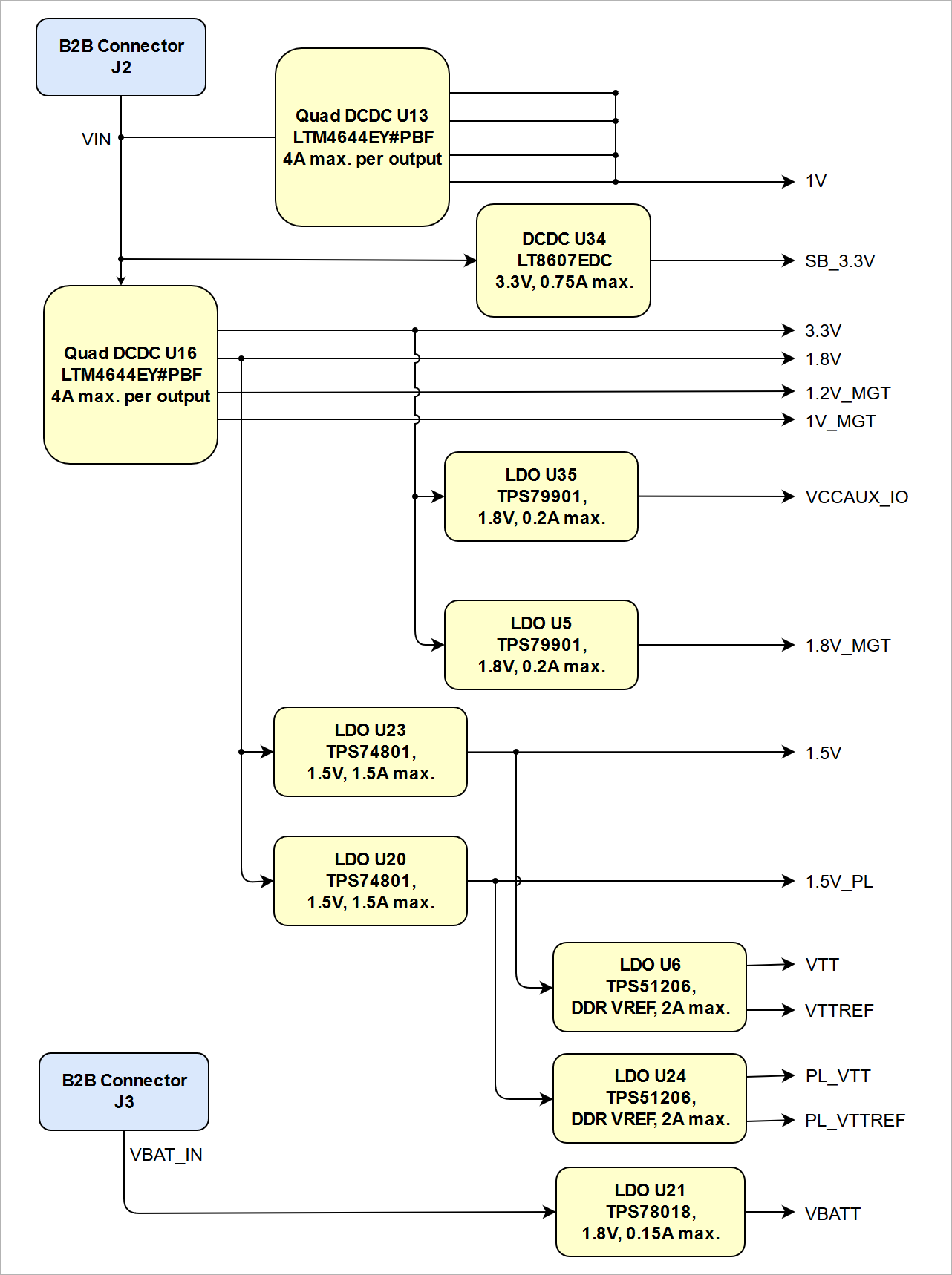
See also Xilinx datasheet DS191 for additional information. User should also check related base board documentation when intending base board design for TE0783 module.
Power-On Sequence
Power-on sequence is handled by the System Controller CPLD using "Power good"-signals from the voltage regulators:
| Scroll Title | ||||||||||||||||||||||||||||||||
|---|---|---|---|---|---|---|---|---|---|---|---|---|---|---|---|---|---|---|---|---|---|---|---|---|---|---|---|---|---|---|---|---|
| ||||||||||||||||||||||||||||||||
|
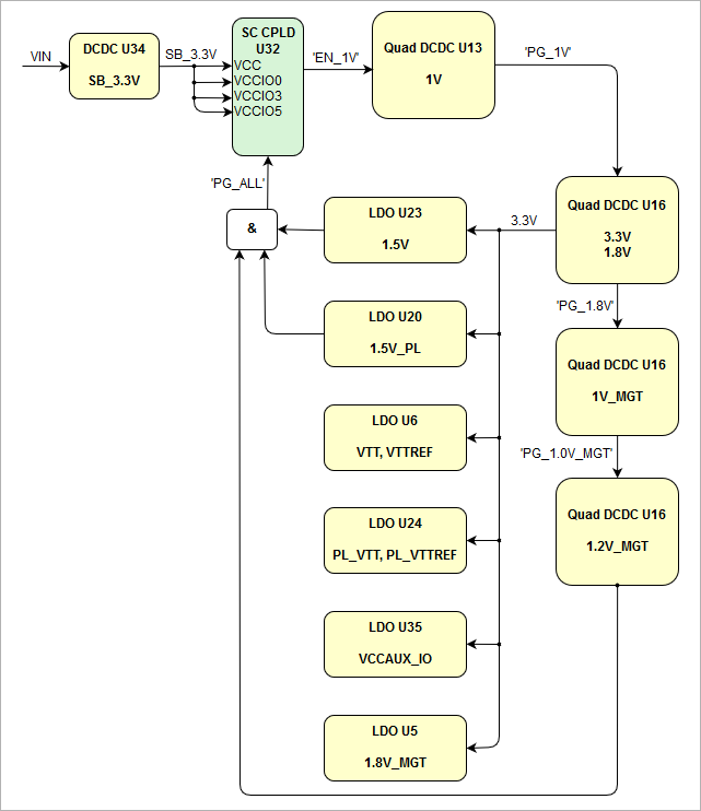
Voltage Monitor Circuit
The voltages '1V' and '3.3V' are monitored by the voltage monitor circuit U27, which generates the PS_POR reset signal if monitored voltages have transient interruptions
Power-On Sequence
The TE0820 SoM meets the recommended criteria to power up the Xilinx Zynq chip properly by keeping a specific sequence of enabling the on-board DC-DC converters dedicated to the particular functional units of the Zynq chip and powering up the on-board voltages.
Following diagram clarifies the sequence of enabling the particular on-board voltages, which will power-up in descending order as listed in the blocks of the diagram:
| Scroll Title | ||||
|---|---|---|---|---|
| ||||
|
...
It is important that all carrier board I/Os are 3-stated at power-on until System Controller CPLD sets PGOOD signal high (B2B connector JM1, pin 30), or 3.3V is present on B2B connector JM2 pins 10 and 12, indicating that all on-module voltages have become stable and module is properly powered up.
...
|

Power Rails
| Power Rail Name on B2B Connector | J1 Pins | J2 Pins | J3 Pins | Direction | Notes |
|---|---|---|---|---|---|
| VIN | - | 165, 166, 167, 168 | - | Input | external power supply voltage |
| C3.3V | - | 147, 148 | - | Input |
| Normally leave unconnected | |||||
| 3.3V | - | 111, 112, 123, 124, 135 136 169, 170, 171, 172 | - | Output | internal 3.3V voltage level |
| 1.8V | 169, 170, |
| 171, 172 | - | - | Output | internal 1.8V voltage level |
| EXT_IO_VCC | 99, 100 | - | - |
| Input |
| SC CPLD bank 1, 2 and 4 voltage | |||||
| VCCIO_10 | - | - | 99, 100 | Input | high range I/O bank voltage |
| VCCIO_11 | - | - | 159, 160 | Input | high range I/O bank voltage |
| VCCIO_12 | - | 159, 160 | - | Input | high range I/O bank voltage |
| VCCIO_13 | - | 99, 100 | - | Input | high range |
| I/O bank voltage | |||||
| VBAT_IN | - | - | 124 | Input | backup battery voltage |
Table 1816: Module power rails
Bank Voltages
| Bank | Schematic Name | Voltage | Range | Notes |
|---|---|---|---|---|
| 0 | - | 3.3 V | - | FPGA configuration |
| 502 | - | 1.5 V | - | DDR3-RAM port |
| 109 / 110 / 111 / 112 | - | 1.2 V | - | MGT |
| 500 |
| - | 3.3 V | - | PS MIO banks | |
| 501 | - | 1.8V | - | PS MIO banks |
| 9 (HR) | - |
| 3. |
| 3 V |
| - | - | |||
| 10 (HR) | VCCIO_10 | user | 1.2V to 3.3V | - |
| 11 (HR) | VCCIO_11 | user | 1.2V to 3.3V | - |
| 12 (HR) | VCCIO_12 | user | 1.2V to 3.3V | - |
| 13 (HR) | VCCIO_13 | user | 1.2V to 3.3V | - |
| 33 (HP) |
| 1.5V_PL | 1. |
| 5 V | - | 64bit DDR3L SD-RAM |
| 34 (HP) |
| 1.5V_PL | 1. |
| 5 V | - |
| 35 (HP) |
| 1. |
| 5V_PL | 1. |
| 5 V | - |
Table 17Table 19: Module I/O bank voltages
...
Board to Board Connectors
| Include Page | ||||
|---|---|---|---|---|
|
Variants Currently In Production
Technical Specifications
Absolute Maximum Ratings
Parameter | Min | Max | Units | Notes |
|---|---|---|---|---|
VIN supply voltage | -0.3 | 15 | V | LTM4644 datasheet |
| VBAT supply voltage | -0.3 |
| 6 | V |
| TPS780180 datasheet | ||||
| PS I/O supply voltage, VCCO_PSIO | -0.5 | 3.6 | V | Xilinx document DS191 |
| PS I/O input voltage | -0.4 | VCCO_PSIO + 0.55 | V | Xilinx document DS191 |
| HP I/O bank supply voltage, VCCO | -0.5 | 2.0 | V | Xilinx document DS191 |
| HP I/O bank input voltage | -0.55 | VCCO + 0.55 | V | Xilinx document DS191 |
| HR I/O bank supply voltage, VCCO | -0.5 | 3.6 | V | Xilinx document DS191 |
| HR I/O bank input voltage | -0.55 | VCCO + 0.55 |
| V | Xilinx document DS191 | |||
| Differential input voltage | -0.4 | 2.625 | V | Xilinx document DS191 |
| MGT reference clocks absolute input voltage | -0.5 | 1.32 | V | Xilinx document DS191 |
| MGT absolute input voltage | -0.5 | 1.26 | V | Xilinx document DS191 |
Voltage on SC CPLD pins | -0.5 | 3.75 | V | Lattice Semiconductor MachXO2 datasheet |
Storage temperature | -40 | +85 | °C | See |
| eMMC MTFC4GACAJCN datasheet |
Table 2018: Module absolute maximum ratings
Recommended Operating Conditions
| Parameter | Min | Max | Units | Notes |
|---|---|---|---|---|
| VIN supply voltage | 11.4 |
| 12.6 | V |
| 12V nominal power supply voltage |
| VBAT supply voltage |
| 2. |
| 2 |
| 5. |
| 5 | V |
| TPS780180 datasheet | ||||
| PS I/O supply voltage, VCCO_PSIO | 1.710 | 3.465 | V | Xilinx document DS191 |
| PS I/O input voltage | –0.20 | VCCO_PSIO + 0.20 | V | Xilinx document DS191 |
| HP I/O banks supply voltage, VCCO | 1.14 | 1.89 | V | Xilinx document DS191 |
| HP I/O banks input voltage | -0.20 | VCCO + 0.20 | V | Xilinx document DS191 |
| HR I/O banks supply voltage, VCCO | 1.14 | 3.465 | V | Xilinx document DS191 |
| HR I/O banks input voltage | -0.20 | VCCO + 0.20 | V | Xilinx document DS191 |
| Differential input voltage | -0.2 | 2.625 | V | Xilinx document DS191 |
| Voltage on SC CPLD pins | -0.3 | 3.6 | V | Lattice Semiconductor MachXO2 datasheet |
| Operating Temperature Range | -40 | 85 | °C | Xilinx document DS191, industrial grade Zynq temperarure range |
Table 2119: Recommended operating conditions
...
| Scroll Title | ||||
|---|---|---|---|---|
| ||||
|
Revision History
Hardware Revision History
| Date | Revision | Notes | PCN Link | Documentation Link |
|---|---|---|---|---|
| - |
| 01 | first production release | - |
| TE0783-01 |
Table 20Table 22: Hardware revision history table
...
| Scroll Title | ||||
|---|---|---|---|---|
| ||||
|
Document Change History
| HTML |
|---|
<!-- Generate new entry: 1.add new row below first 2.Copy "Page Information Macro(date)" Macro-Preview, Metadata Version number, Author Name and description to the empty row. Important Revision number must be the same as the Wiki document revision number 3.Update Metadata = "Page Information Macro (current-version)" Preview+1 and add Author and change description. --> |
Date | Revision | Contributors | Description | ||||||||||||||||||||||||||
|---|---|---|---|---|---|---|---|---|---|---|---|---|---|---|---|---|---|---|---|---|---|---|---|---|---|---|---|---|---|
|
|
|
| ||||||||||||||||||||||||||
| 2018-08-07 | v.18 | Ali Naseri |
| ||||||||||||||||||||||||||
| -- | all |
|
|
Table 21Table 23: Document change history
Disclaimer
| Include Page | ||||
|---|---|---|---|---|
|
Overview
Content Tools