Page History
...
...
...
| Scroll pdf ignore | |
|---|---|
Table of Contents
|
Overview
...
...
...
...
...
...
...
...
...
...
|
Main Components
| Page properties | ||||
|---|---|---|---|---|
| ||||
Notes :
|
| Scroll Title | |||||||||||||||||
|---|---|---|---|---|---|---|---|---|---|---|---|---|---|---|---|---|---|
| |||||||||||||||||
|
...
...
|
- ...
- ...
- ...
Initial Delivery State
| Page properties | ||||
|---|---|---|---|---|
| ||||
Notes : Only components like EEPROM, QSPI flash can be initialized by default at manufacture. If there is no components which might have initial data ( possible on carrier) you must keep the table empty |
...
| anchor | Table_OV_IDS |
|---|---|
| title | Initial delivery state of programmable devices on the module |
...
Storage device name
...
Content
...
Notes
...
Configuration Signals
| Page properties | ||||
|---|---|---|---|---|
| ||||
|
...
...
...
MODE Signal State
...
Signals, Interfaces and Pins
| Page properties | ||||
|---|---|---|---|---|
| ||||
Notes :
|
Board to Board (B2B) I/Os
FPGA bank number and number of I/O signals connected to the B2B connector:
...
| anchor | Table_SIP_B2B |
|---|---|
| title | General PL I/O to B2B connectors information |
...
JTAG Interface
JTAG access to the TEB0835 SoM through B2B connector JM2.
...
...
SPI_CS , SPI_DQ0... SPI_DQ3
SPI_SCK
...
| anchor | Table_SIP_MIOs |
|---|---|
| title | MIOs pins |
...
...
B2B Connector
...
MIO Pins
...
| hidden | true |
|---|---|
| id | Comments |
you must fill the table below with group of MIOs which are connected to a specific components or peripherals, you do not have to specify pins in B2B, Just mention which B2B is connected to MIOs. The rest is clear in the Schematic.
Example:
...
...
...
...
...
| hidden | true |
|---|---|
| id | Comments |
you must fill the table below with group of Test Point which are indicated as TP in a schematic. If there is no Test Point remarked in the schematic, delet the Test Point section.
Example:
...
| anchor | Table_SIP_TPs |
|---|---|
| title | Test Points Information |
...
On-board Peripherals
| Page properties | ||||
|---|---|---|---|---|
| ||||
Notes :
|
...
| hidden | true |
|---|---|
| id | Comments |
Notes :
...
...
...
...
Quad SPI Flash Memory
| Page properties | ||||
|---|---|---|---|---|
| ||||
Notes : Minimum and Maximum density of quad SPI flash must be mentioned for other assembly options. |
...
| anchor | Table_OBP_SPI |
|---|---|
| title | Quad SPI interface MIOs and pins |
...
...
...
...
...
...
...
...
...
...
...
| anchor | Table_OBP_EEP |
|---|---|
| title | I2C EEPROM interface MIOs and pins |
...
...
...
...
...
...
LEDs
...
| anchor | Table_OBP_LED |
|---|---|
| title | On-board LEDs |
...
DDR3 SDRAM
| Page properties | ||||
|---|---|---|---|---|
| ||||
Notes : Minimum and Maximum density of DDR3 SDRAM must be mentioned for other assembly options. (pay attention to supported address length for DDR3) |
The TE???? SoM has ??? GByte volatile DDR3 SDRAM IC for storing user application code and data.
- Part number:
- Supply voltage:
- Speed:
- NOR Flash
- Temperature:
Ethernet
...
...
...
...
...
CAN Transceiver
...
| anchor | Table_OBP_CAN |
|---|---|
| title | CAN Tranciever interface MIOs |
...
| anchor | Table_OBP_CLK |
|---|---|
| title | Osillators |
...
Programmable Clock Generator
There is a programmable clock generator on-board (U??) provided in order to generate variable clocks for the module. Programming can be done using I2C via PIN header J??. The I2C Address is 0x??.
...
| anchor | Table_OBP_PCLK |
|---|---|
| title | Programmable Clock Generator Inputs and Outputs |
| Scroll Table Layout | ||||||||||||
|---|---|---|---|---|---|---|---|---|---|---|---|---|
|
...
IN0
...
XAXB
...
Power and Power-On Sequence
...
| hidden | true |
|---|---|
| id | Comments |
In 'Power and Power-on Sequence' section there are three important digrams which must be drawn:
- Power on-sequence
- Power distribution
- Voltage monitoring circuit
| Note |
|---|
For more information regarding how to draw diagram, Please refer to "Diagram Drawing Guidline" . |
Power Supply
Power supply with minimum current capability of xx A for system startup is recommended.
Power Consumption
...
| anchor | Table_PWR_PC |
|---|---|
| title | Power Consumption |
...
...
* TBD - To Be Determined
Power Distribution Dependencies
...
| anchor | Figure_PWR_PD |
|---|---|
| title | Power Distribution |
...
| Scroll Only |
|---|
|
...
...
...
...
...
Voltage Monitor Circuit
...
| anchor | Figure_PWR_VMC |
|---|---|
| title | Voltage Monitor Circuit |
| Scroll Ignore |
|---|
Create DrawIO object here: Attention if you copy from other page, objects are only linked. |
| Scroll Only |
|---|
image link to the generate DrawIO PNG file of this page. This is a workaround until scroll pdf export bug is fixed |
Power Rails
...
| anchor | Table_PWR_PR |
|---|---|
| title | Module power rails. |
...
B2B Connector
JM1 Pin
...
B2B Connector
JM2 Pin
...
B2B Connector
JM3 Pin
...
Bank Voltages
...
Create DrawIO object here: Attention if you copy from other page, objects are only linked.
| Scroll Only |
|---|
image link to the generate DrawIO PNG file of this page. This is a workaround until scroll pdf export bug is fixed |
...
...
...
...
...
...
...
| hidden | true |
|---|---|
| id | Comments |
...
use "include page" macro and link to the general B2B connector page of the module series,
...
? x ? modules use two or three Samtec Micro Tiger Eye Connector on the bottom side.
3 x REF-??????? (compatible to ????????), (?? pins, ?? per row)
Operating Temperature: -??°C ~ ??°C
Current Rating: ??A per ContactNumber of Positions: ??
Number of Rows: ??
Technical Specifications
Absolute Maximum Ratings
...
| anchor | Table_TS_AMR |
|---|---|
| title | PS absolute maximum ratings |
...
...
Recommended Operating Conditions
...
...
...
...
...
...
...
...
...
Physical Dimensions
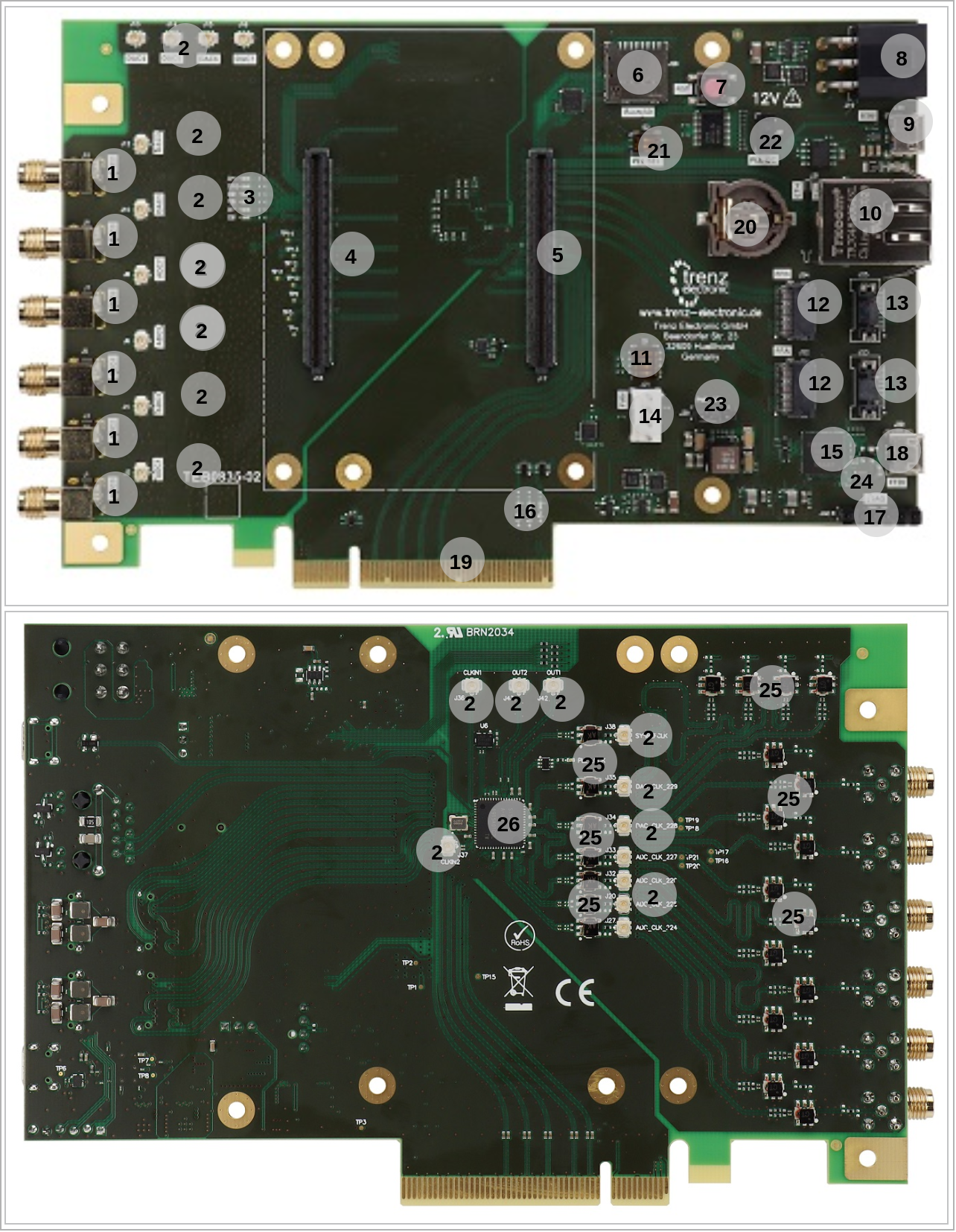
Module size: ?? mm × ?? mm. Please download the assembly diagram for exact numbers.
Mating height with standard connectors: ? mm.
PCB thickness: ?? mm.
...
| hidden | true |
|---|---|
| id | Comments |
In 'Physical Dimension' section, top and bottom view of module must be inserted, information regarding physical dimensions can be obtained through webpage for product in Shop.Trenz, (Download> Documents> Assembly part) for every SoM.
For Example: for Module TE0728, Physical Dimension information can be captured by snipping tools from the link below:
| Note |
|---|
For more information regarding how to draw diagram, Please refer to "Diagram Drawing Guidline" . |
|
Pin Header 1x3
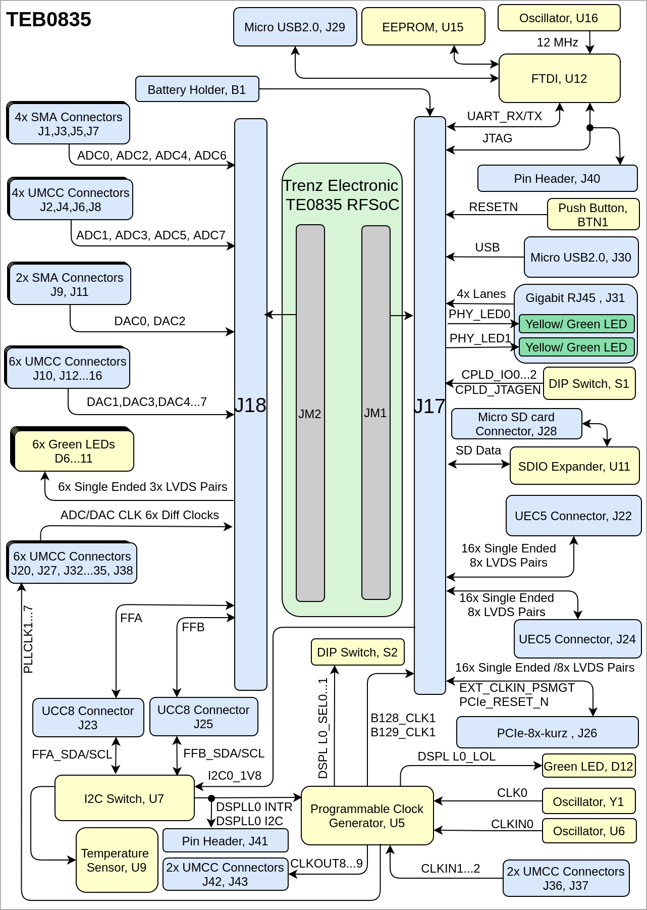
There is a 1x3 Pin Header J41, it provides access to I2C signals which are connected to I2C Switch, U7.
| Scroll Title | ||||||||||||||||||||||||||||||||||
|---|---|---|---|---|---|---|---|---|---|---|---|---|---|---|---|---|---|---|---|---|---|---|---|---|---|---|---|---|---|---|---|---|---|---|
| ||||||||||||||||||||||||||||||||||
|
Jumper
There is a Jumper J39 provided for setting the DCDC_EN between two signal level as the following.
| Scroll Title | ||||||||||||||||||||||||||||||||||
|---|---|---|---|---|---|---|---|---|---|---|---|---|---|---|---|---|---|---|---|---|---|---|---|---|---|---|---|---|---|---|---|---|---|---|
| ||||||||||||||||||||||||||||||||||
|
I2C Addresses
| Scroll Title | ||||||||||||||||||||||||||||||
|---|---|---|---|---|---|---|---|---|---|---|---|---|---|---|---|---|---|---|---|---|---|---|---|---|---|---|---|---|---|---|
| ||||||||||||||||||||||||||||||
|
Test Points
| Page properties | ||||||||
|---|---|---|---|---|---|---|---|---|
| ||||||||
you must fill the table below with group of Test Point which are indicated as TP in a schematic. If there is no Test Point remarked in the schematic, delet the Test Point section. Example:
|
| Scroll Title | ||||||||||||||||||||||||||||||||||||||||||||||||||||||||||||||||||||||||||||||||||||||||||||||||||||||
|---|---|---|---|---|---|---|---|---|---|---|---|---|---|---|---|---|---|---|---|---|---|---|---|---|---|---|---|---|---|---|---|---|---|---|---|---|---|---|---|---|---|---|---|---|---|---|---|---|---|---|---|---|---|---|---|---|---|---|---|---|---|---|---|---|---|---|---|---|---|---|---|---|---|---|---|---|---|---|---|---|---|---|---|---|---|---|---|---|---|---|---|---|---|---|---|---|---|---|---|---|---|---|
| ||||||||||||||||||||||||||||||||||||||||||||||||||||||||||||||||||||||||||||||||||||||||||||||||||||||
|
On-board Peripherals
| Page properties | ||||
|---|---|---|---|---|
| ||||
Notes :
|
| Page properties | ||||
|---|---|---|---|---|
| ||||
Notes : In the on-board peripheral table "chip/Interface" must be linked to the corresponding chapter or subsection |
| Scroll Title | |||||||||||||||||||||||||||||||||||||||||||||
|---|---|---|---|---|---|---|---|---|---|---|---|---|---|---|---|---|---|---|---|---|---|---|---|---|---|---|---|---|---|---|---|---|---|---|---|---|---|---|---|---|---|---|---|---|---|
| |||||||||||||||||||||||||||||||||||||||||||||
|
EEPROM
There is an EEPROM U15 provided in order to store the FTDI configuration.
| Scroll Title | ||||||||||||||||||||||||||||||||||
|---|---|---|---|---|---|---|---|---|---|---|---|---|---|---|---|---|---|---|---|---|---|---|---|---|---|---|---|---|---|---|---|---|---|---|
| ||||||||||||||||||||||||||||||||||
|
DIP Switch
There are two DIP Switches S1, S2 provided for boot mode and manual input select of programmable clock generator. For more information please refer to Configuration Signal Section
| Scroll Title | |||||||||||||||||||||||||||||||||||||||||||||||||
|---|---|---|---|---|---|---|---|---|---|---|---|---|---|---|---|---|---|---|---|---|---|---|---|---|---|---|---|---|---|---|---|---|---|---|---|---|---|---|---|---|---|---|---|---|---|---|---|---|---|
| |||||||||||||||||||||||||||||||||||||||||||||||||
|
Temperature Sensor
There is a temperature sensor IC U9 provided to capture the temperature and provides an alert when cooling is needed. the temperature IC is connected to I2C bus at address 0x4C.
| Scroll Title | ||||||||||||||||||||||||||||||||||||||||||||||||||||||
|---|---|---|---|---|---|---|---|---|---|---|---|---|---|---|---|---|---|---|---|---|---|---|---|---|---|---|---|---|---|---|---|---|---|---|---|---|---|---|---|---|---|---|---|---|---|---|---|---|---|---|---|---|---|---|
| ||||||||||||||||||||||||||||||||||||||||||||||||||||||
|
FTDI
The FTDI chip U12 converts signals from USB2 to a variety of standard serial and parallel interfaces. Refer to the FTDI data sheet to get information about the capacity of the FT2232H chip. FTDI FT2232H chip is used in MPPSE mode for JTAG, 2 I/O's of Channel B are routed to B2B J17 and must be used as UART.
The configuration of FTDI FT2232H chip is pre-programmed on the EEPROM U15.
| Scroll Title | |||||||||||||||||||||||||||||||||||||||||||||||
|---|---|---|---|---|---|---|---|---|---|---|---|---|---|---|---|---|---|---|---|---|---|---|---|---|---|---|---|---|---|---|---|---|---|---|---|---|---|---|---|---|---|---|---|---|---|---|---|
| |||||||||||||||||||||||||||||||||||||||||||||||
|
Push Button
| Scroll Title | ||||||||||||||||||||||||||
|---|---|---|---|---|---|---|---|---|---|---|---|---|---|---|---|---|---|---|---|---|---|---|---|---|---|---|
| ||||||||||||||||||||||||||
|
LEDs
| Scroll Title | ||||||||||||||||||||||||||||||||||||||||||||||||
|---|---|---|---|---|---|---|---|---|---|---|---|---|---|---|---|---|---|---|---|---|---|---|---|---|---|---|---|---|---|---|---|---|---|---|---|---|---|---|---|---|---|---|---|---|---|---|---|---|
| ||||||||||||||||||||||||||||||||||||||||||||||||
|
Clock Sources
| Scroll Title | ||||||||||||||||||||||||||||||||||||||
|---|---|---|---|---|---|---|---|---|---|---|---|---|---|---|---|---|---|---|---|---|---|---|---|---|---|---|---|---|---|---|---|---|---|---|---|---|---|---|
| ||||||||||||||||||||||||||||||||||||||
|
Programmable Clock Generator
There is a programmable clock generator on-board (U5) provided in order to generate variable clocks for the module. The I2C Address is 0x68.
| Scroll Title | |||||||||||||||||||||||||||||||||||||||||||||||||||||||||||||||||||||||||||||||||||||||||||||||||||||||||||||||||||||||||||||||||||||||||||
|---|---|---|---|---|---|---|---|---|---|---|---|---|---|---|---|---|---|---|---|---|---|---|---|---|---|---|---|---|---|---|---|---|---|---|---|---|---|---|---|---|---|---|---|---|---|---|---|---|---|---|---|---|---|---|---|---|---|---|---|---|---|---|---|---|---|---|---|---|---|---|---|---|---|---|---|---|---|---|---|---|---|---|---|---|---|---|---|---|---|---|---|---|---|---|---|---|---|---|---|---|---|---|---|---|---|---|---|---|---|---|---|---|---|---|---|---|---|---|---|---|---|---|---|---|---|---|---|---|---|---|---|---|---|---|---|---|---|---|---|
| |||||||||||||||||||||||||||||||||||||||||||||||||||||||||||||||||||||||||||||||||||||||||||||||||||||||||||||||||||||||||||||||||||||||||||
|
Power and Power-On Sequence
| Page properties | ||||
|---|---|---|---|---|
| ||||
In 'Power and Power-on Sequence' section there are three important digrams which must be drawn:
|
Power Supply
Power supply with minimum current capability of 3 A for system startup is recommended.
Power Consumption
| Scroll Title | ||||||||||||||||||||||
|---|---|---|---|---|---|---|---|---|---|---|---|---|---|---|---|---|---|---|---|---|---|---|
| ||||||||||||||||||||||
|
* TBD - To Be Determined
Power Distribution Dependencies
| Scroll Title | ||||||||||||||||||||||||||||||||
|---|---|---|---|---|---|---|---|---|---|---|---|---|---|---|---|---|---|---|---|---|---|---|---|---|---|---|---|---|---|---|---|---|
| ||||||||||||||||||||||||||||||||
|
Power-On Sequence
| Scroll Title | ||||||||||||||||||||||||||||
|---|---|---|---|---|---|---|---|---|---|---|---|---|---|---|---|---|---|---|---|---|---|---|---|---|---|---|---|---|
| ||||||||||||||||||||||||||||
|
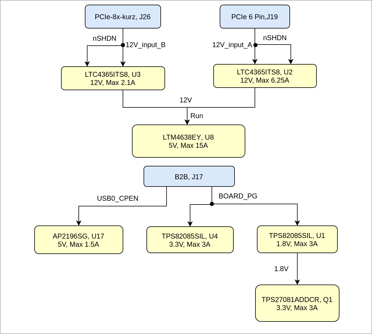
Power Rails
| Scroll Title | ||||||||||||||||||||||||||||||||||||||
|---|---|---|---|---|---|---|---|---|---|---|---|---|---|---|---|---|---|---|---|---|---|---|---|---|---|---|---|---|---|---|---|---|---|---|---|---|---|---|
| ||||||||||||||||||||||||||||||||||||||
|
Board to Board Connectors
| Page properties | ||||||
|---|---|---|---|---|---|---|
| ||||||
|
| Include Page | ||||
|---|---|---|---|---|
|
Technical Specifications
Absolute Maximum Ratings
| Scroll Title | |||||||||||||||||||||||||||||||||||||||||||
|---|---|---|---|---|---|---|---|---|---|---|---|---|---|---|---|---|---|---|---|---|---|---|---|---|---|---|---|---|---|---|---|---|---|---|---|---|---|---|---|---|---|---|---|
| |||||||||||||||||||||||||||||||||||||||||||
|
Recommended Operating Conditions
Operating temperature range depends also on customer design and cooling solution. Please contact us for options.
| Scroll Title | |||||||||||||||||||||||||||||||||||||||||||
|---|---|---|---|---|---|---|---|---|---|---|---|---|---|---|---|---|---|---|---|---|---|---|---|---|---|---|---|---|---|---|---|---|---|---|---|---|---|---|---|---|---|---|---|
| |||||||||||||||||||||||||||||||||||||||||||
|
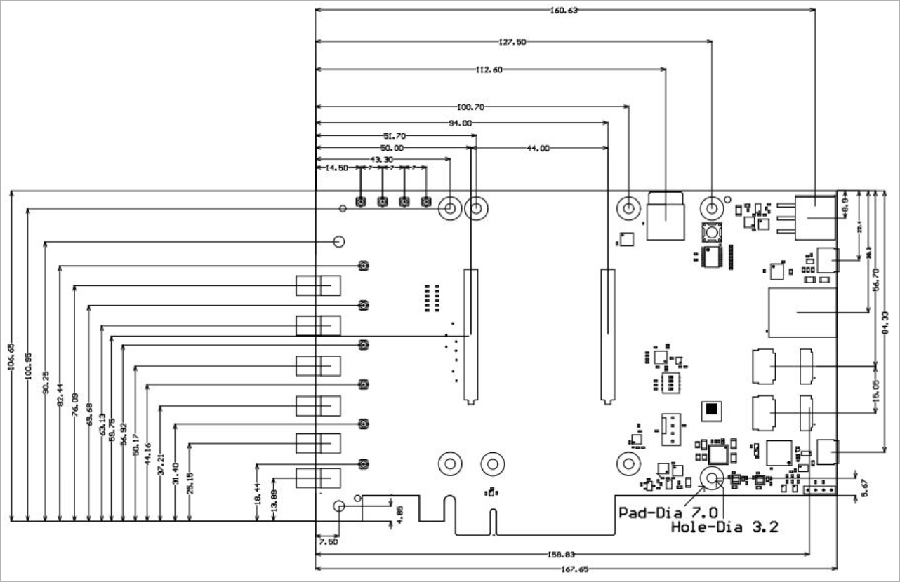
Physical Dimensions
Module size: 106.6 mm × 167.7 mm. Please download the assembly diagram for exact numbers.
Mating height with standard connectors: 5 mm.
PCB thickness: 1.5 mm.
| Page properties | ||||
|---|---|---|---|---|
| ||||
In 'Physical Dimension' section, top and bottom view of module must be inserted, information regarding physical dimensions can be obtained through webpage for product in Shop.Trenz, (Download> Documents> Assembly part) for every SoM. For Example: for Module TE0728, Physical Dimension information can be captured by snipping tools from the link below:
|
| Scroll Title | |||||||||||||||||||||||||||||||||||||||||||||||
|---|---|---|---|---|---|---|---|---|---|---|---|---|---|---|---|---|---|---|---|---|---|---|---|---|---|---|---|---|---|---|---|---|---|---|---|---|---|---|---|---|---|---|---|---|---|---|---|
| |||||||||||||||||||||||||||||||||||||||||||||||
|
Currently Offered Variants
| Page properties | ||||
|---|---|---|---|---|
| ||||
Set correct link to the shop page overview table of the product on English and German. Example for TE0728: ENG Page: https://shop.trenz-electronic.de/en/Products/Trenz-Electronic/TE07XX-Zynq-SoC/TE0728-Zynq-SoC/ DEU Page: https: |
...
| anchor | Figure_TS_PD |
|---|---|
| title | Physical Dimension |
...
| Scroll Only | ||||||||||||||
|---|---|---|---|---|---|---|---|---|---|---|---|---|---|---|
| ||||||||||||||
|
Currently Offered Variants
...
| hidden | true |
|---|---|
| id | Comments |
Set correct link to the shop page overview table of the product on English and German.
Example for TE0728:
...
...
...
...
...
...
For Baseboards or modules, where no overview page is available (and revision number is coded in the direct link) use shop search link, e.g. TE0706:
ENG Page: https://shop.trenz-electronic.de/en/search?sSearch=TE0706
...
...
...
...
...
...
...
...
Revision History
Hardware Revision History
| Page properties | ||||
|---|---|---|---|---|
| ||||
Set correct links to download arrier, e.g. TE0706 REV02: TE0706-02 -> https://shop.trenz-electronic.de/Download/?path=Trenz_Electronic/Modules_and_Module_Carriers/4x5/4x5_Carriers/TE0706/REV02/Documents Note:
|
...
| anchor | Table_RH_HRH |
|---|---|
| title | Hardware Revision History |
...
...
...
...
|
Document Change History
| Page properties | ||||
|---|---|---|---|---|
| ||||
|
| Scroll Title | |||||||||||||||||||||||||||||||||||||||||||||||||||
|---|---|---|---|---|---|---|---|---|---|---|---|---|---|---|---|---|---|---|---|---|---|---|---|---|---|---|---|---|---|---|---|---|---|---|---|---|---|---|---|---|---|---|---|---|---|---|---|---|---|---|---|
| |||||||||||||||||||||||||||||||||||||||||||||||||||
|
...
Overview
Content Tools