Page History
| Custom_table_size_100 |
|---|
| Page properties | ||||||||||||||||||||||||||||||||||||
|---|---|---|---|---|---|---|---|---|---|---|---|---|---|---|---|---|---|---|---|---|---|---|---|---|---|---|---|---|---|---|---|---|---|---|---|---|
| ||||||||||||||||||||||||||||||||||||
Template Change history:
|
| Page properties | ||||||||||||||||||||||||||||||||||||||||||||
|---|---|---|---|---|---|---|---|---|---|---|---|---|---|---|---|---|---|---|---|---|---|---|---|---|---|---|---|---|---|---|---|---|---|---|---|---|---|---|---|---|---|---|---|---|
| ||||||||||||||||||||||||||||||||||||||||||||
Important General Note:
|
| Page properties | ||||
|---|---|---|---|---|
| ||||
----------------------------------------------------------------------- |
| Page properties | ||||
|---|---|---|---|---|
| ||||
Note for Download Link of the Scroll ignore macro:
|
| Scroll Ignore |
|---|
Overview
The Trenz Electronic AM0010 module is an industrialgrade module based on AMD Xilinx.
Refer to http://trenz.org/AM0010am0010-info for the current online version of this manual and other available documentation.
| Page properties | ||||
|---|---|---|---|---|
| ||||
Notes :
|
Key Features
| Page properties | ||||
|---|---|---|---|---|
| ||||
Note: → See examples fro different types <Series Name> TRM Template section examples#%3CSeriesName%3ETRMTemplatesectionexamples-KeyFeatures |
| Excerpt |
|---|
|
Block Diagram
| Page properties | ||||||
|---|---|---|---|---|---|---|
| ||||||
add drawIO object in Scroll Ignore section and add reference image in Scroll Only.
|
| Scroll Title | ||||||||||||||||||||||||||||
|---|---|---|---|---|---|---|---|---|---|---|---|---|---|---|---|---|---|---|---|---|---|---|---|---|---|---|---|---|
| ||||||||||||||||||||||||||||
|
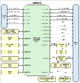
Main Components
| Page properties | ||||
|---|---|---|---|---|
| ||||
Notes :
|
| Scroll Title | ||||||||||||||||||||||||||||
|---|---|---|---|---|---|---|---|---|---|---|---|---|---|---|---|---|---|---|---|---|---|---|---|---|---|---|---|---|
| ||||||||||||||||||||||||||||
|
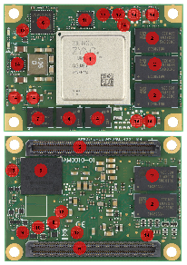
- FPGA, U1
- DDR4, U2, U3, U9, U12, U14
- eMMC, U17
- Quad SPI Flash, U6, U7
- Connector, J5, J6
- Ethernet Transceiver, U8
- HyperFlash, U16
- EEPROM, U15
- OPTIGA Trust M, U27
- CryptoAuthentication, U24
- USB Transceiver, U10
- Oscillator, U13, U14, U30, U31, U32
- Analog Multiplexer, U38
- Power Supply, U5, U11, U18, U19, U20, U21, U22, U23, U28
Initial Delivery State
| Page properties | ||||
|---|---|---|---|---|
| ||||
|
| Scroll Title | ||||||||||||||||||||||||||||||||||||
|---|---|---|---|---|---|---|---|---|---|---|---|---|---|---|---|---|---|---|---|---|---|---|---|---|---|---|---|---|---|---|---|---|---|---|---|---|
| ||||||||||||||||||||||||||||||||||||
|
Signals, Interfaces and Pins
| Page properties | ||||
|---|---|---|---|---|
| ||||
For subsection examples see: <Series Name> TRM Template section examples#%3CSeriesName%3ETRMTemplatesectionexamples-Signals,InterfacesandPins
|
Connectors
| Scroll Title | |||||||||||||||||||||||||||||||||||||||||||||||||||||||||||||||||||||||||||||||||||||||||||||||||||||||
|---|---|---|---|---|---|---|---|---|---|---|---|---|---|---|---|---|---|---|---|---|---|---|---|---|---|---|---|---|---|---|---|---|---|---|---|---|---|---|---|---|---|---|---|---|---|---|---|---|---|---|---|---|---|---|---|---|---|---|---|---|---|---|---|---|---|---|---|---|---|---|---|---|---|---|---|---|---|---|---|---|---|---|---|---|---|---|---|---|---|---|---|---|---|---|---|---|---|---|---|---|---|---|---|
| |||||||||||||||||||||||||||||||||||||||||||||||||||||||||||||||||||||||||||||||||||||||||||||||||||||||
1) IO CNT depends on assembly variant. E.g. the MGTs are not available for all FPGAs |
Test Points
| Page properties | ||||||||
|---|---|---|---|---|---|---|---|---|
| ||||||||
you must fill the table below with group of Test Point which are indicated as TP in a schematic. If there is no Test Point remarked in the schematic, delet the Test Point section. Example:
|
| Scroll Title | ||||||||||||||||||||||||||||||||||||||||||||||||||||||||||||||||||||||||||||||||||||
|---|---|---|---|---|---|---|---|---|---|---|---|---|---|---|---|---|---|---|---|---|---|---|---|---|---|---|---|---|---|---|---|---|---|---|---|---|---|---|---|---|---|---|---|---|---|---|---|---|---|---|---|---|---|---|---|---|---|---|---|---|---|---|---|---|---|---|---|---|---|---|---|---|---|---|---|---|---|---|---|---|---|---|---|---|
| ||||||||||||||||||||||||||||||||||||||||||||||||||||||||||||||||||||||||||||||||||||
|
On-board Peripherals
| Page properties | ||||||||
|---|---|---|---|---|---|---|---|---|
| ||||||||
Notes : In the on-board peripheral table "chip/Interface" must be linked to the corresponding chapter or subsection by assigning advance link using: #NameOfTheSection Example:
|
| Scroll Title | ||||||||||||||||||||||||||||||||||||||||||||||||||||||||||||||||||||||||||||||||||
|---|---|---|---|---|---|---|---|---|---|---|---|---|---|---|---|---|---|---|---|---|---|---|---|---|---|---|---|---|---|---|---|---|---|---|---|---|---|---|---|---|---|---|---|---|---|---|---|---|---|---|---|---|---|---|---|---|---|---|---|---|---|---|---|---|---|---|---|---|---|---|---|---|---|---|---|---|---|---|---|---|---|---|
| ||||||||||||||||||||||||||||||||||||||||||||||||||||||||||||||||||||||||||||||||||
|
| Page properties | ||||
|---|---|---|---|---|
| ||||
For example subsections see: <Series Name> TRM Template section examples#%3CSeriesName%3ETRMTemplatesectionexamples-On-boardPeripherals |
Configuration and System Control Signals
| Page properties | ||||
|---|---|---|---|---|
| ||||
|
| Scroll Title | ||||||||||||||||||||||||||||||||||||||||||||||||||||||||||||||||||||||||||||||||||
|---|---|---|---|---|---|---|---|---|---|---|---|---|---|---|---|---|---|---|---|---|---|---|---|---|---|---|---|---|---|---|---|---|---|---|---|---|---|---|---|---|---|---|---|---|---|---|---|---|---|---|---|---|---|---|---|---|---|---|---|---|---|---|---|---|---|---|---|---|---|---|---|---|---|---|---|---|---|---|---|---|---|---|
| ||||||||||||||||||||||||||||||||||||||||||||||||||||||||||||||||||||||||||||||||||
1) Direction:
1) Direction:
2) See UG1085 for additional information. 3) See Recommended Operating Conditions. |
Power and Power-On Sequence
| Page properties | ||||
|---|---|---|---|---|
| ||||
Enter the default value for power supply and startup of the module here.
Link to Schematics, for power images or more details |
Power Rails
| Page properties | ||||
|---|---|---|---|---|
| ||||
List of all Powerrails which are accessible by the customer
|
| Scroll Title | ||||||||||||||||||||||||||||||||||||||||||||||||||||||||||||||
|---|---|---|---|---|---|---|---|---|---|---|---|---|---|---|---|---|---|---|---|---|---|---|---|---|---|---|---|---|---|---|---|---|---|---|---|---|---|---|---|---|---|---|---|---|---|---|---|---|---|---|---|---|---|---|---|---|---|---|---|---|---|---|
| ||||||||||||||||||||||||||||||||||||||||||||||||||||||||||||||
1) Direction:
|
Recommended Power up Sequencing
| Page properties | ||||
|---|---|---|---|---|
| ||||
List baseboard design hints for final baseboard development. |
| Scroll Title | |||||||||||||||||||||||||||||||||||||||||||||||||||||||||||||||||||||||||||||||||||||||||||||||||||||||||||||||||||||||||||||||||||||||||||||||||||||||||||||||
|---|---|---|---|---|---|---|---|---|---|---|---|---|---|---|---|---|---|---|---|---|---|---|---|---|---|---|---|---|---|---|---|---|---|---|---|---|---|---|---|---|---|---|---|---|---|---|---|---|---|---|---|---|---|---|---|---|---|---|---|---|---|---|---|---|---|---|---|---|---|---|---|---|---|---|---|---|---|---|---|---|---|---|---|---|---|---|---|---|---|---|---|---|---|---|---|---|---|---|---|---|---|---|---|---|---|---|---|---|---|---|---|---|---|---|---|---|---|---|---|---|---|---|---|---|---|---|---|---|---|---|---|---|---|---|---|---|---|---|---|---|---|---|---|---|---|---|---|---|---|---|---|---|---|---|---|---|---|---|---|
| |||||||||||||||||||||||||||||||||||||||||||||||||||||||||||||||||||||||||||||||||||||||||||||||||||||||||||||||||||||||||||||||||||||||||||||||||||||||||||||||
Priority | Net name | Voltage Range | Pull-up/down | Description | Notes | Pin | Preparation | TDI/TCK/TDO/TMS | V_IO_CFG | - | JTAG interface. | J6.D51, J6.D52, J6.D54, J6.D55 | Preparation | MODE0...3 | V_IO_CFG | - | Boot mode setup. Do not float. | Hardwiring possible. Consider debug options. Boot Mode options are descriped in AMD Xilinx documentation. J6.C54, J6.C55, J6.C56, J6.C57 | Preparation | DX_P / DX_N | - | - | MPSoC temperature measurement. J6.D56, J6.D57 | 1 | V_BAT | -
see table "Module Power Rails" |
(on module)
(Do not tie "PWR_EN" to VDD directly. | This signal could be tied to GND within this module.) J6.D58 |
4 | 3.3V / 1.8V | - | - | Module generated voltages. | see table "Module Power Rails" | 5
(on module)
J6.D59 | 6 | V_IO_W01 / V_IO_W45 / V_IO_X01 / V_IO_W3 / V_IO_X3 / V_IO_CFG
see table "Module Power Rails" |
7 | DONE | V_IO_CFG | PU, V_IO_CFG | (on module) PL configuration monitoring. | This signal states the PL configuration according to AMD Xilinx documentation. | J6.C53 | 7 | PS_SRST# | V_IO_CFG | PU, V_IO_CFG Module reset. | This signal initiate a system reset according to AMD Xilins documentation. | J6.C58 | 8 | PS_POR# | V_IO_CFG | PU,
Power-on reset. | Needs to held at zero until all PS power supplies meet voltage requirements and the PS_CLK reference is within specification. When deasserted the PS begins the boot process. | J6.C59 | 8 | RST_M2C# | V_IO_CFG | PU, 3.3 V Baseboard peripheral reset. | This signals resets module peripheral and can / should be used for baseboard peripheral reset. | J6.B58
1) (optional) 2) (on module) 3) See DS925 for additional information. |
Board to Board Connectors
| Page properties | ||||||
|---|---|---|---|---|---|---|
| ||||||
|
| Include Page | ||||
|---|---|---|---|---|
|
Technical Specifications
Absolute Maximum Ratings *)
| Scroll Title | |||||||||||||||||||||||||||||||||||||||||||||||||||||||||||||||
|---|---|---|---|---|---|---|---|---|---|---|---|---|---|---|---|---|---|---|---|---|---|---|---|---|---|---|---|---|---|---|---|---|---|---|---|---|---|---|---|---|---|---|---|---|---|---|---|---|---|---|---|---|---|---|---|---|---|---|---|---|---|---|---|
| |||||||||||||||||||||||||||||||||||||||||||||||||||||||||||||||
1) It is possible to use a resistor instead of the LDO but then, consider the different min (-0.500 V) / max (2.000 V) values. |
*) Stresses beyond those listed under Absolute Maximum Ratings may cause permanent damage to the device. These are stress ratings only, which do not imply functional operation of the device at these
or any other conditions beyond those indicated under Recommended Operating Condition. Exposure to absolute-maximum rated conditions for extended periods may affect device reliability.
Recommended Operating Conditions
This TRM is generic for all variants. Temperature range can be differ depending on the assembly version. Voltage range is mostly the same during variants (exceptions are possible, depending on custom request)
Operating temperature range depends also on customer design and cooling solution. Please contact us for options.
- Variants of modules are described here: Article Number Information
- Modules with commercial temperature grade are equipped with components that cover at least the range of 0°C to 75°C
- Modules with extended temperature grade are equipped with components that cover at least the range of 0°C to 85°C
- Modules with industrial temperature grade are equipped with components that cover at least the range of -40°C to 85°C
- The actual operating temperature range will depend on the FPGA / SoC design / usage and cooling and other variables.
| Scroll Title | |||||||||||||||||||||||||||||||||||||||||||||||||||||||||||||||
|---|---|---|---|---|---|---|---|---|---|---|---|---|---|---|---|---|---|---|---|---|---|---|---|---|---|---|---|---|---|---|---|---|---|---|---|---|---|---|---|---|---|---|---|---|---|---|---|---|---|---|---|---|---|---|---|---|---|---|---|---|---|---|---|
| |||||||||||||||||||||||||||||||||||||||||||||||||||||||||||||||
1) Using a resistor instead of the LDO is possible which leads to different min (1.2 V) / max (1.89 V) values. |
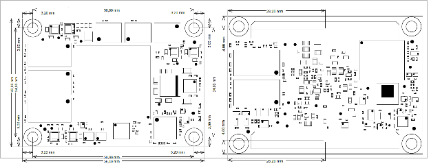
Physical Dimensions
Module size: 56.4 mm × 40 mm. Please download the assembly diagram for exact numbers.
Mating height with standard connectors: 5 mm.
PCB thickness: 2 mm.
| Page properties | ||||
|---|---|---|---|---|
| ||||
In 'Physical Dimension' section, top and bottom view of module must be inserted, information regarding physical dimensions can be obtained through webpage for product in Shop.Trenz, (Download> Documents> Assembly part) for every SoM. For Example: for Module TE0728, Physical Dimension information can be captured by snipping tools from the link below:
|
| Scroll Title | |||||||||||||||||||||||||||||||||||||||||
|---|---|---|---|---|---|---|---|---|---|---|---|---|---|---|---|---|---|---|---|---|---|---|---|---|---|---|---|---|---|---|---|---|---|---|---|---|---|---|---|---|---|
| |||||||||||||||||||||||||||||||||||||||||
|
Currently Offered Variants
| Page properties | ||||
|---|---|---|---|---|
| ||||
Set correct link to the shop page overview table of the product on English and German. Example for TE0706: ENG Page: https://shop.trenz-electronic.de/en/search?sSearch=TE0706 DEU Page: https://shop.trenz-electronic.de/de/search?sSearch=TE0706 |
| Scroll Title | ||||||||||||||||||||||
|---|---|---|---|---|---|---|---|---|---|---|---|---|---|---|---|---|---|---|---|---|---|---|
| ||||||||||||||||||||||
| ||||||||||||||||||||||
Revision History
Hardware Revision History
| Page properties | ||||||||
|---|---|---|---|---|---|---|---|---|
| ||||||||
Set correct links to download Carrier, e.g. TE0706 REV02: TE0706-02 -> https://shop.trenz-electronic.de/Download/?path=Trenz_Electronic/Modules_and_Module_Carriers/4x5/4x5_Carriers/TE0706/REV02/Documents Note:
|
| Scroll Title | |||||||||||||||||||||||||||||||||||||||||||||
|---|---|---|---|---|---|---|---|---|---|---|---|---|---|---|---|---|---|---|---|---|---|---|---|---|---|---|---|---|---|---|---|---|---|---|---|---|---|---|---|---|---|---|---|---|---|
| |||||||||||||||||||||||||||||||||||||||||||||
|

| Scroll Title | ||||||||||||||||||||||||||
|---|---|---|---|---|---|---|---|---|---|---|---|---|---|---|---|---|---|---|---|---|---|---|---|---|---|---|
| ||||||||||||||||||||||||||
|
Hardware revision number can be found on the PCB board together with the module model number separated by the dash.
Document Change History
| Page properties | ||||
|---|---|---|---|---|
| ||||
|
| Scroll Title | ||||||||||||||||||||||||||||||||||||||||||||||||||||||||||||||||||||
|---|---|---|---|---|---|---|---|---|---|---|---|---|---|---|---|---|---|---|---|---|---|---|---|---|---|---|---|---|---|---|---|---|---|---|---|---|---|---|---|---|---|---|---|---|---|---|---|---|---|---|---|---|---|---|---|---|---|---|---|---|---|---|---|---|---|---|---|---|
| ||||||||||||||||||||||||||||||||||||||||||||||||||||||||||||||||||||
|
Disclaimer
| Include Page | ||||
|---|---|---|---|---|
|
| Scroll Only | ||
|---|---|---|
|
| Scroll pdf ignore | ||||||
|---|---|---|---|---|---|---|
|
Overview
Content Tools