...
| Page properties |
|---|
|
Note for Download Link of the Scroll ignore macro: |
| Scroll pdf ignore |
|---|
Table of Contents |
Overview
The carrier board TEB0745 was especially designed and developed for the use of Trenz Electronic module TE0745.
...
Key Features
- Module: Form factor 20 cm x 23,1 cm
- Trenz Electronic Module TE0745
- Temperature: -40 to 85 °C
- On Board: TE0745 Module Socket (3 x Samtec connectors) over ARKZ950/2 connecting
- terminal
- 1 x EMI Network Filter
- 3 x Variable Step Down Regulator Module (VDRM) with head sink
- 2 x Synchronous Buck Regulator
- 2 x Button (User / Reset)
- 2 x LED (Green)
- Interfaces:
- 1 x XMOD (TE0790) Pin Header (JTAG / UART)
- 1 x Pin Header (JTAG)
- 1 x microSD connector
- 1 x RJ45 Ethernet connector
- 1 x USB Host Connector
- 8 x SFP-Connector
- 6 x Pin Header 50 pol. (FPGA Bank I/O's and Power)
- 6 x Pin Header 12 pol. (FPGA Bank I/O's and Power)
- 1 x battery holder
- 2 x DIP Switch Array (VCC_HR_B / Modi)
- 2 x Button (User / Reset)
- 2 x LED (Green)Dimension: 200 mm x 231 mm
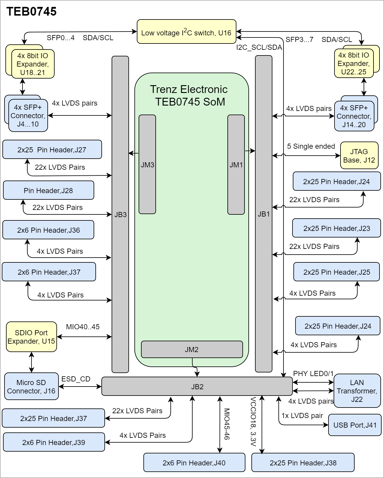
Block Diagram
| Page properties |
|---|
|
add drawIO object here.
|
...
| Scroll Title |
|---|
| anchor | Figure_OV_BD |
|---|
| title | TEB0745 block diagram |
|---|
|
| Scroll Ignore |
|---|
| draw.io Diagram |
|---|
| border | false |
|---|
| viewerToolbar | true |
|---|
| |
|---|
| fitWindow | false |
|---|
| diagramDisplayName | |
|---|
| lbox | true |
|---|
| revision | 1221 |
|---|
| diagramName | TEB0745_OV_BD |
|---|
| simpleViewer | false |
|---|
| width | |
|---|
| links | auto |
|---|
| tbstyle | hidden |
|---|
| diagramWidth | 640 |
|---|
|
|
| Scroll Only |
|---|
|
|
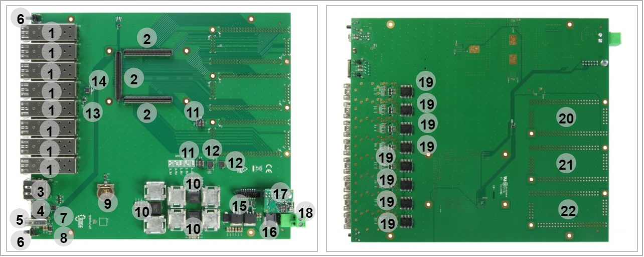
Main Components
| Page properties |
|---|
|
Notes : - Picture of the PCB (top and bottom side) with labels of important components
- Add List below
|
...
| Scroll Title |
|---|
| anchor | Figure_OV_BD |
|---|
| title | TExxxx TEB0745 main components |
|---|
|
| Scroll Ignore |
|---|
| draw.io Diagram |
|---|
| border | false |
|---|
| viewerToolbar | true |
|---|
| |
|---|
| fitWindow | false |
|---|
| diagramDisplayName | |
|---|
| lbox | true |
|---|
| revision | 56 |
|---|
| diagramName | TEB0745_Figure_OV_MC |
|---|
| simpleViewer | false |
|---|
| width | |
|---|
| links | auto |
|---|
| tbstyle | hidden |
|---|
| diagramWidth | 641642 |
|---|
|
|
| Scroll Only |
|---|
|
|
- SFP+ Connector, J4 J6 J8 J10 J13 J15 J18 J20
- Board to Board Connector (B2B), J1 J2 J3
- RJ45 Gigabit Ethernet connector, J22
- SD card connector, J16
- USB connector, J41
- Push Button, S2 S3
- SDIO port expander, U15
- Power distribution switch, U4
- Battery holder, B1
- Mag I3C power, U26 U12 U5
- Push bottun switch, S1 S4
- Buck regulator, U6 U7
- I2C EEPROM, U33
- Low voltage chanel I2C switch, U16
- Overvoltage, undervoltage, reversesupply protection controller, U13
- EMI suppression filter, U29
- JTAG interface, J12
- Power jack, J31
- 8bit IO expandor for I2C bus, U18 U25
- Pin Headers J23...26 (Not Assembled)
- Pin Headers J27-J28-J32-J36 (Not Assembled)
- Pin Headers J37...40 (Not Assembled)
Initial Delivery State
| Page properties |
|---|
|
Notes : Only components like EEPROM, QSPI flash and DDR3 can be initialized by default at manufacture. If there is no components which might have initial data ( possible on carrier) you must keep the table empty |
...
| Scroll Title |
|---|
| anchor | Table_OV_IDS |
|---|
| title | Initial delivery state of programmable devices on the module |
|---|
|
| Scroll Table Layout |
|---|
| orientation | portrait |
|---|
| sortDirection | ASC |
|---|
| repeatTableHeaders | default |
|---|
| style | |
|---|
| widths | |
|---|
| sortByColumn | 1 |
|---|
| sortEnabled | false |
|---|
| cellHighlighting | true |
|---|
|
Storage device name | Content | Notes |
|---|
| EEPROMNot Programmed | EUI-64 number programmed | Can be used for MAC |
|
Configuration Signals
| Page properties |
|---|
|
- Overview of Boot Mode, Reset, Enables.
|
...
| Scroll Title |
|---|
| anchor | Table_OV_BP |
|---|
| title | Boot process. |
|---|
|
| Scroll Table Layout |
|---|
| orientation | portrait |
|---|
| sortDirection | ASC |
|---|
| repeatTableHeaders | default |
|---|
| style | |
|---|
| widths | |
|---|
| sortByColumn | 1 |
|---|
| sortEnabled | false |
|---|
| cellHighlighting | true |
|---|
|
MODE Signal State | ConnectConnected to | B2B | Status | Boot Mode |
|---|
BOOTMODE | S1 | J2-133 | Open | QSPI | | Short | SD Card |
|
...
| Scroll Title |
|---|
| anchor | Table_OV_RST |
|---|
| title | Reset process. |
|---|
|
| Scroll Table Layout |
|---|
| orientation | portrait |
|---|
| sortDirection | ASC |
|---|
| repeatTableHeaders | default |
|---|
| style | |
|---|
| widths | |
|---|
| sortByColumn | 1 |
|---|
| sortEnabled | false |
|---|
| cellHighlighting | true |
|---|
|
SignalPS_SRST | J2-152 | PS Reset | | RST_IN_N | Push Button, S2 | J2-131 |
General
|
Signals, Interfaces and Pins
| Page properties |
|---|
|
Notes : - For carrier or stand-alone boards use subsection for every connector type (add designator on description, not on the subsection title), for example:
- For modules which needs carrier use only classes and refer to B2B connector if more than one is used, for example
|
Board to Board (B2B) I/Os
FPGA bank number and number of I/O signals connected to the B2B connector:
| Scroll Title |
|---|
| anchor | Table_SIP_B2B |
|---|
| title | General PL I/O to B2B connectors information |
|---|
|
| Scroll Table Layout |
|---|
| orientation | portrait |
|---|
| sortDirection | ASC |
|---|
| repeatTableHeaders | default |
|---|
| style | |
|---|
| widths | |
|---|
| sortByColumn | 1 |
|---|
| sortEnabled | false |
|---|
| cellHighlighting | true |
|---|
|
onnected | B2B Connector | Interfaces | Number of I/O | Notes |
|---|
J1
| User I/O | 48 singel ended, 24 Differential 2 singel ended | Connected to Bank 13 | 48 singel ended, 24 Differential 2 singel ended |
C| Connected to Bank 12 | | JTAG Interface | 5 single ended | TCK, TDI, TMS, TDO, JTAG_EN | | SFP+ Connector | 8 Diff | SPF4....7_RX_N/P , SPF4....7_TX_N/P | J2
| Ethernet PHY | 4 Differential |
| | 2 single ended | PHY_LED0...1 | | USB | 1 Differential | OTG_N/P | | Control Signals | 3 single ended | PS_SRST, BOOTMODE, RST_IN_N | | Power Control Signal | 2 single ended | PWR_PS_OK, PWR_PL_OK | | I2C Bus | 2 single ended | I2C_SDA, I2C_SCL | | User I/O | 4 single ended | MIO12...15 | J3
| User I/O | 6 Single ended | MIO46...51 | | SD Card Connector | 6 Single ended | SD_CLK, SD_CMD, SD_DAT0...3 (MIO40...45) | | SFP+ Connector | 8 Differential |
SPF0| SPF0....3_RX_N/P , SPF0....3_TX_N/P |
|
...
JTAG access to the TEB0745 SoM is available through B2B connector JB1 and JB2. JTAG_EN is connected to J1-138, JTAG_EN can be activated through DIP Switch S1-B2.
| Scroll Title |
|---|
| anchor | Table_SIP_JTG |
|---|
| title | JTAG pins connection |
|---|
|
| Scroll Table Layout |
|---|
| orientation | portrait |
|---|
| sortDirection | ASC |
|---|
| repeatTableHeaders | default |
|---|
| style | |
|---|
| widths | |
|---|
| sortByColumn | 1 |
|---|
| sortEnabled | false |
|---|
| cellHighlighting | true |
|---|
|
| Designator | Connected to | B2B Pin | XMOD Header JB1 | Note |
|---|
| A | MIO15 | J2-129 | JB1-3 | UART |
Txd - input| TX - Input to the module | | B | MIO14 | J2-127 | JB1-7 | UART |
Rxd | RX - Output of the module | | C | TCK | J1-143 | JB1-4 | JTAG interface signal | | D | TDO | J1-145 | JB1-8 | JTAG interface signal | | F | TDI | J1-142 | JB1-10 | JTAG interface signal | | H | TMS | J1-144 | JB1-12 | JTAG interface signal | | G | RST_IN_N | J2-131 | JB1-11 | RESET will be connected to Push Button on JTAG Programmer |
|
...
There is a DIP switch, S2, on TE0790 adapter which must be set as following.
| Scroll Title |
|---|
| anchor | Table_OBPSIP_I2CXmod_RTCDIP |
|---|
| title | I2C Address for RTC Xmod Adapter DIP-Switch Setting Description |
|---|
|
| Scroll Table Layout |
|---|
| orientation | portrait |
|---|
| sortDirection | ASC |
|---|
| repeatTableHeaders | default |
|---|
| style | |
|---|
| widths | |
|---|
| sortByColumn | 1 |
|---|
| sortEnabled | false |
|---|
| cellHighlighting | true |
|---|
|
|
| I2C Device | I2C Address | Designator | Notes |
|---|
| I2C_EXP | 0x72 | U16 | SFP 0-9 |
EEPROM | 0x51 | U33 | I/O EXP | 0x20...27 | U18...25 |
On-board Peripherals
| Page properties |
|---|
|
Notes : - add subsection for every component which is important for design, for example:
- Two 100 Mbit Ethernet Transciever PHY
- USB PHY
- Programmable Clock Generator
- Oscillators
- eMMCs
- RTC
- FTDI
- ...
- DIP-Switches
- Buttons
- LEDs
|
SD Card Socket
Power supply voltage for SD card holder is 3.3V.
...
| anchor | Table_OBP_SPI |
|---|
| title | Quad SPI interface MIOs and pins |
|---|
...
RJ45 Connector
Etherneth Socket is connected to Board to Board (B2B) JM2.
...
| anchor | Table_OBP_RJ45 |
|---|
| title | LAN Transformer |
|---|
...
| DIP Switch,S2 | Default | Description |
|---|
| 1 | ON | Update Mode JTAG access to SC CPLD only | | 2 | OFF | Must be always in OFF state. | | 3 | OFF | VIO is supplied from Module | | 4 | ON | 3.3V from XMOD |
|
SFP+ Connectors
The TEB0745 is equipped with 8 SFP+ Connectors,
| Scroll Title |
|---|
| anchor | Table_OBP_SFP |
|---|
| title | SFP Connectors |
|---|
|
| Scroll Table Layout |
|---|
| orientation | portrait |
|---|
| sortDirection | ASC |
|---|
| repeatTableHeaders | default |
|---|
| style | |
|---|
| widths | |
|---|
| sortByColumn | 1 |
|---|
| sortEnabled | false |
|---|
| cellHighlighting | true |
|---|
|
| Pin | Connected to | Notes |
|---|
| SFP+ , J4 | SFP+, J6 | SFP+, J8 | SFP+, J10 | SFP+, J13 | SFP+, J15 | SFP+, J18 | SFP+, J20 |
|---|
| TD+ | B2B, J3 | B2B, J3 | B2B, J3 | B2B, J3 | B2B, J1 | B2B, J1 | B2B, J1 | B2B, J1 | GT | | TD- | B2B, J3 | B2B, J3 | B2B, J3 | B2B, J3 | B2B, J1 | B2B, J1 | B2B, J1 | B2B, J1 | GT | | RD+ | B2B, J3 | B2B, J3 | B2B, J3 | B2B, J3 | B2B, J1 | B2B, J1 | B2B, J1 | B2B, J1 | GT | | RD- | B2B, J3 | B2B, J3 | B2B, J3 | B2B, J3 | B2B, J1 | B2B, J1 | B2B, J1 | B2B, J1 | GT | | TX FAULT | IO Exp, U18 | IO Exp, U19 | IO Exp, U20 | IO Exp, U21 | IO Exp, U22 | IO Exp, U23 | IO Exp, U24 | IO Exp, U25 | SFP_CTRL | | TX DISABLE | IO Exp, U18 | IO Exp, U19 | IO Exp, U20 | IO Exp, U21 | IO Exp, U22 | IO Exp, U23 | IO Exp, U24 | IO Exp, U25 | SFP_CTRL | | MOD-DEF2 | IO Exp, U18 | IO Exp, U19 | IO Exp, U20 | IO Exp, U21 | IO Exp, U22 | IO Exp, U23 | IO Exp, U24 | IO Exp, U25 | SFP_CTRL | | MOD-DEF1 | IO Exp, U18 | IO Exp, U19 | IO Exp, U20 | IO Exp, U21 | IO Exp, U22 | IO Exp, U23 | IO Exp, U24 | IO Exp, U25 | SFP_CTRL | | MOD-DEF0 | IO Exp, U18 | IO Exp, U19 | IO Exp, U20 | IO Exp, U21 | IO Exp, U22 | IO Exp, U23 | IO Exp, U24 | IO Exp, U25 | SFP_CTRL | | RS0 | IO Exp, U18 | IO Exp, U19 | IO Exp, U20 | IO Exp, U21 | IO Exp, U22 | IO Exp, U23 | IO Exp, U24 | IO Exp, U25 | SFP_CTRL | | LOS | IO Exp, U18 | IO Exp, U19 | IO Exp, U20 | IO Exp, U21 | IO Exp, U22 | IO Exp, U23 | IO Exp, U24 | IO Exp, U25 | SFP_CTRL | | RS1 | IO Exp, U18 | IO Exp, U19 | IO Exp, U20 | IO Exp, U21 | IO Exp, U22 | IO Exp, U23 | IO Exp, U24 | IO Exp, U25 | SFP_CTRL |
|
SD Card Socket
Power supply voltage for SD card holder is 3.3V.
| Scroll Title |
|---|
| anchor | Table_OBP_SDcard |
|---|
| title | SD card interface MIOs and pins |
|---|
|
|
...
EEPROM
...
| anchor | Table_OBP_EEP |
|---|
| title | I2C EEPROM interface MIOs and pins |
|---|
...
DIP Switches
There are two DIP Switches S1,S4.
| Scroll Title |
|---|
| anchor | Table_OBP_DIP |
|---|
| title | DIP Switch S1 |
|---|
|
| scroll-tablelayout |
|---|
| orientation | portrait |
|---|
| sortDirection | ASC |
|---|
| repeatTableHeaders | default |
|---|
| style | |
|---|
| widths | |
|---|
| sortByColumn | 1 |
|---|
| sortEnabled | false |
|---|
| cellHighlighting | true |
|---|
|
DesignatorNoteS1ABootMode| J2-133 | S1B | JTAG_EN | J1-148 | S1C | - | S1D | PS_SW | J2-123| J3-150 |
| | SD_CMD | MIO41 | J3-152 |
| | SD_DAT0 | MIO42 | J3-154 |
| | SD_DAT1 | MIO43 | J3-156 |
| | SD_DAT2 | MIO44 | J3-158 |
| | SD_DAT3 | MIO45 | J3-160 |
|
|
RJ45 Connector
Ethernet Socket is connected to Board to Board (B2B) JM2.
| Scroll Title |
|---|
| anchor | Table_OBP_DIPRJ45 |
|---|
| title | DIP Switch S4LAN Transformer |
|---|
|
| Scroll Table Layout |
|---|
| orientation | portrait |
|---|
| sortDirection | ASC |
|---|
| repeatTableHeaders | default |
|---|
| style | |
|---|
| widths | |
|---|
| sortByColumn | 1 |
|---|
| sortEnabled | false |
|---|
| cellHighlighting | true |
|---|
|
DesignatorConnected to| B2B | Note | | S4A | VADJ_VS2 | - | Connected to 5 V | | S4B | VADJ_VS1 | - | Connected to 5 V | S4C | VADJ_VS0 | Connected to 5 V | | S4D | - | - | - | |
Push Button
...
| Notes |
|---|
| PHY_MDIO0_P | J2-120 |
| | PHY_MDIO_N | J2-122 |
| | PHY_MDIO1_P | J2-126 |
| | PHY_MDIO1_N | J2-128 |
| | PHY_MDIO2_P | J2-132 |
| | PHY_MDIO2_N | J2-134 |
| | PHY_MDIO3_P | J2-138 |
| | PHY_MDIO3_N | J2-140 |
| | PHY_LED0 | J2-144 |
| | PHY_LED1 | J2-146 |
|
|
Test Points
| Scroll Title |
|---|
| anchor | Table_OBPSIP_Push_ButtonTestPoint |
|---|
| title | On-board push button =sTest Points Information |
|---|
|
| Scroll Table Layout |
|---|
| orientation | portrait |
|---|
| sortDirection | ASC |
|---|
| repeatTableHeaders | default |
|---|
| style | |
|---|
| widths | |
|---|
| sortByColumn | 1 |
|---|
| sortEnabled | false |
|---|
| cellHighlighting | true |
|---|
|
DesignatorConnected toActive Level| Note | S3 | USR_BTN | J3-153 | Active high | | S2 | RST_IN_N | J2-131 | Active high | General Reset | |
LEDs
...
| anchor | Table_OBP_LED |
|---|
| title | On-board LEDs |
|---|
| TP 1 | 5V | - |
| | TP 2 | VBAT_IN | J1-146 |
| | TP 3 | VCCIO18V | J2- J3 |
| | TP 4 | VCC_HR_B | J1 |
| | TP 5-9 | GND | - |
| | TP 10 | PS_1.8V | J2 |
| | TP 11 | VCC_HR_B | J1 |
| | TP 12 | 3.3V | J1- J2 |
| | TP 13 | - | - |
| | TP 14 | - | - |
| | TP 15 | PWR_PL_OK | J2- 135 |
| | TP 16 | PWR_PS_OK | J2-139 |
| | TP 17 | 24V_FUSED | - |
| | TP 18 | 3.3V_SFP | - |
|
|
On-board Peripherals
...
| Page properties |
|---|
| In 'Power and Power-on Sequence' section there are three important digrams which must be drawn:
- Power on-sequence
- Power distribution
- Voltage monitoring circuit
Power Supply
Power supply with minimum current capability of xx A for system startup is recommended.
Power Consumption
Notes : - add subsection for every component which is important for design, for example:
- Two 100 Mbit Ethernet Transciever PHY
- USB PHY
- Programmable Clock Generator
- Oscillators
- eMMCs
- RTC
- FTDI
- ...
- DIP-Switches
- Buttons
- LEDs
|
| Page properties |
|---|
|
Notes : In the on-board peripheral table "chip/Interface" must be linked to the corresponding chapter or subsection |
| Scroll Title |
|---|
| anchor | Table_OBP |
|---|
| title | On board peripherals |
|---|
|
| Scroll Title |
|---|
| anchor | Table_PWR_PC |
|---|
| title | Power Consumption |
|---|
|
| Scroll Table Layout |
|---|
| orientation | portrait |
|---|
| sortDirection | ASC |
|---|
| repeatTableHeaders | default | style |
|---|
| widths | sortByColumn | 1 |
|---|
| sortEnabled | false |
|---|
| cellHighlighting | true |
|---|
|
|
| Power Input Pin | Typical Current |
|---|
| VIN | TBD* |
* TBD - To Be Determined
Power Distribution Dependencies
EEPROM
| scrollscroll-title |
|---|
| anchor | FigureTable_PWROBP_PDEEP |
|---|
| title | Power DistributionI2C EEPROM interface MIOs and pins |
|---|
|
| ignoredrawioborderfalseviewerToolbartruefitWindowfalsediagramDisplayNamelboxtruerevision6 |
| diagramName | TEB0745_PWR_PD |
|---|
| simpleViewer | false |
|---|
width | | links | auto |
|---|
| tbstyle | hidden |
|---|
| diagramWidth | 641 |
|---|
| Scroll Only |
|---|
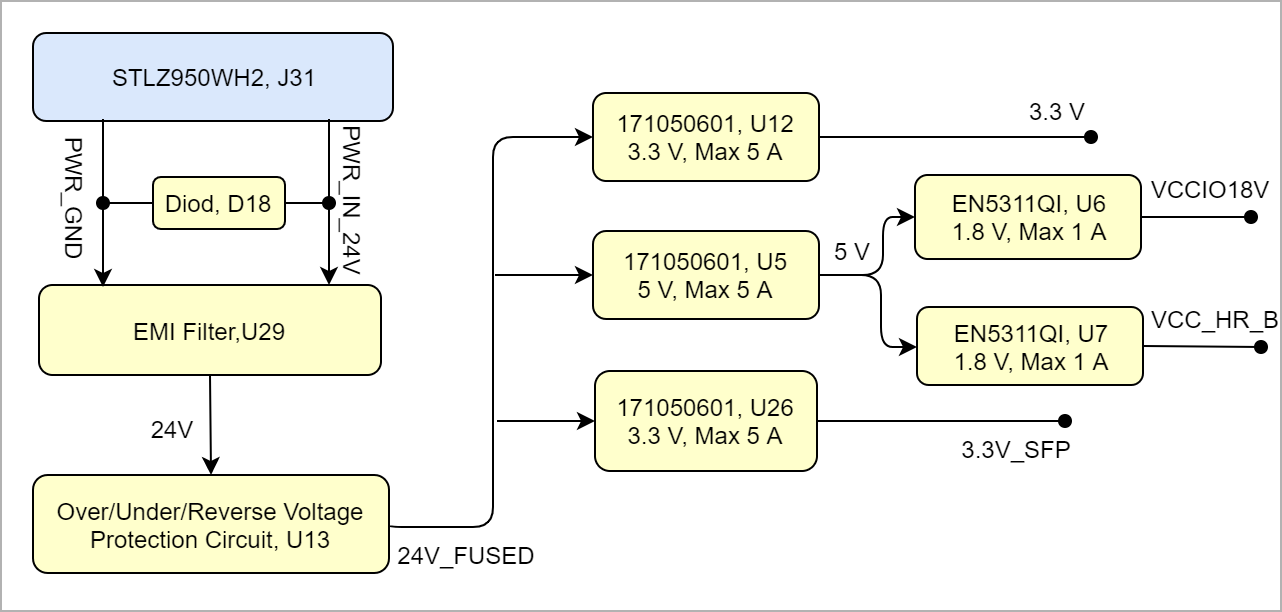 Image Removed Image Removed
|
Power-On Sequence
| MIO Pin | Schematic | B2B | Notes |
|---|
| MIO10 | I2C_SCL | J2-119 |
| | MIO11 | I2C_SDA | J2-121 |
|
|
| Scroll Title |
|---|
| anchor | FigureTable_OBP_PWRI2C_PSEEPROM |
|---|
| title | Power SequencyI2C address for EEPROM |
|---|
|
| ignoredrawiobordertrueviewerToolbartruefitWindowfalse |
| diagramName | TEB0745_PWR_PS |
|---|
simpleViewer | widthdiagramWidth641 | | revision | 3 |
|---|
| Scroll Only |
|---|
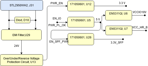 Image Removed Image Removed
|
...
| I2C Device | Designator | I2C Address | Notes |
|---|
| EEPROM | U33 | 0x51 |
|
|
DIP Switches
There are two DIP Switches S1,S4.
| Scroll Title |
|---|
| anchor | FigureTable_PWROBP_VMCDIP |
|---|
| title | Voltage Monitor CircuitDIP Switch S1 |
|---|
|
| ignore |
Create DrawIO object here: Attention if you copy from other page, objects are only linked. |
| Scroll Only |
|---|
image link to the generate DrawIO PNG file of this page. This is a workaround until scroll pdf export bug is fixed |
Power Rails
| tablelayout |
|---|
| orientation | portrait |
|---|
| sortDirection | ASC |
|---|
| repeatTableHeaders | default |
|---|
|
|
| Scroll Title |
|---|
| anchor | Table_PWR_PR |
|---|
| title | Module power rails. |
|---|
|
| Scroll Table Layout |
|---|
| orientation | portrait |
|---|
| sortDirection | ASC |
|---|
| repeatTableHeaders | default |
|---|
| style | |
|---|
| widths | |
|---|
| sortByColumn | 1 |
|---|
| sortEnabled | false |
|---|
| cellHighlighting | true |
|---|
|
|
| Power Rail Name | VCC / VCCIO | Direction | Notes |
|---|
| JB1 | 3.3V | IN | PL_VIN |
| VCC_HR_B | IN | VCCIO_12, VCCIO_13 |
| JB2 | VCCIO18V | IN | VCCIO_34, VCCIO_35 |
| PS_1.8V | OUT | PWR_OUT |
| 3.3V | IN | PS_3.3V |
JB3 | VCCIO18V | IN | PWR_IN_VCCIO_33 |
Bank Voltages
| Designator | Connected to | B2B | Note |
|---|
| S1-A | BootMode | J2-133 |
| | S1-B | JTAG_EN | J1-148 |
| | S1-C | - |
|
| | S1-D | PS_SW | J2-123 |
|
|
VCC_HR_B voltage can be selected using DIP Switch S4 .
| Scroll Title |
|---|
| anchor | Table_OBP_DIP |
|---|
| title | DIP Switch S4 |
|---|
|
| Scroll Title |
|---|
| anchor | Table_PWR_BV |
|---|
| title | Zynq SoC bank voltages. |
|---|
|
| Scroll Table Layout |
|---|
| orientation | portrait |
|---|
| sortDirection | ASC |
|---|
| repeatTableHeaders | default |
|---|
| style | |
|---|
| widths | |
|---|
| sortByColumn | 1 |
|---|
| sortEnabled | false |
|---|
| cellHighlighting | true |
|---|
|
| Schematic Name | | Notes |
|---|
|
...
...
| S4-1 | S4-2 | S4-3 | S4-4 | Power VCC_HR_B | Notes |
|---|
| OFF | OFF | OFF | N.C. | 1,8V |
| | OFF | OFF | ON | N.C. | 1,5V |
| | OFF | ON | OFF | N.C. | 3,3V |
| | OFF | ON | ON | N.C. | 2,5V |
| | ON | OFF | OFF | N.C. | 0,8V |
| | ON | OFF | ON | N.C. | Do not use |
| | ON | ON | OFF | N.C. | 1,25V |
| | ON | ON | ON | N.C. | 1,2V |
|
|
I2C Switch
There is a I2C Switch on the TEB0745 which can be used in order to controll the SPF+ Connectors.
use "include page" macro and link to the general B2B connector page of the module series,
...
? x ? modules use two or three Samtec Micro Tiger Eye Connector on the bottom side.
3 x REF-??????? (compatible to ????????), (?? pins, ?? per row)
Operating Temperature: -??°C ~ ??°C
Current Rating: ??A per ContactNumber of Positions: ??
Number of Rows: ??
Technical Specifications
Absolute Maximum Ratings
...
| anchor | Table_TS_AMR |
|---|
| title | PS absolute maximum ratings |
|---|
...
Recommended Operating Conditions
Operating temperature range depends also on customer design and cooling solution. Please contact us for options.
| Scroll Title |
|---|
| anchor | Table_TSOBP_ROCI2CSW |
|---|
| title | Recommended operating conditions.I2C Switch |
|---|
|
| Scroll Table Layout |
|---|
| orientation | portrait |
|---|
| sortDirection | ASC |
|---|
| repeatTableHeaders | default |
|---|
| style | |
|---|
| widths | |
|---|
| sortByColumn | 1 |
|---|
| sortEnabled | false |
|---|
| cellHighlighting | true |
|---|
|
ParameterMinMaxUnits| Reference Document | V | See ???? datasheets. | V | See Xilinx ???? datasheet. | V | See Xilinx ???? datasheet. | V | See Xilinx ???? datasheet. | V | See Xilinx ???? datasheet. | V | See Xilinx ???? datasheet. | V | See Xilinx ???? datasheet. | °C | See Xilinx ???? datasheet. | °C | See Xilinx ???? datasheet. | |
Physical Dimensions
Module size: ?? mm × ?? mm. Please download the assembly diagram for exact numbers.
Mating height with standard connectors: ? mm.
PCB thickness: ?? mm.
| VCC | 3.3V |
|
| | SCL | I2C_SCL | B2B, J2 |
| | SDA | I2C_SDA | B2B, J2 |
| | nRESET | I2C_RST | Voltage Translator, U34 |
| | A0 | GND | Low | I2C address is 0x72 | | A1 | 3.3V | High | I2C address is 0x72 | | A2 | GND | Low | I2C address is 0x72 | | SD0/ SC0 | SFP0_SDA / SFP0_SDA | SFP+ Connector, J4 |
| | SD1/ SC1 | SFP1_SDA / SFP1_SDA | SFP+ Connector, J6 |
| | SD2/ SC2 | SFP2_SDA / SFP2_SDA | SFP+ Connector, J8 |
| | SD3/ SC3 | SFP3_SDA / SFP3_SDA | SFP+ Connector, J10 |
| | SD4/ SC4 | SFP4_SDA / SFP4_SDA | SFP+ Connector, J13 |
| | SD5/ SC5 | SFP5_SDA / SFP5_SDA | SFP+ Connector, J15 |
| | SD6/ SC6 | SFP6_SDA / SFP6_SDA | SFP+ Connector, J18 |
| | SD7/ SC7 | SFP7_SDA / SFP7_SDA | SFP+ Connector, J20 |
|
| Page properties |
|---|
|
In 'Physical Dimension' section, top and button view of moduloe must be insterted, information regarding physical dimention can be obtained through webpage for product in Shop.Trenz, (Download> Documents> Assembly part)for every SoM. For Example: for Module TE0728, Physical Dimension information can be captured by snipping tools from the link below: https://www.trenz-electronic.de/fileadmin/docs/Trenz_Electronic/Modules_and_Module_Carriers/5.2x7.6/TE0745/REV02/Documents/AD-TE0745-02-30-1I.PDF | Note |
|---|
For more information regarding how to draw diagram, Please refer to "Diagram Drawing Guidline" .
|
| Scroll Title |
|---|
| anchor | FigureTable_TSOBP_PDI2CSWADD |
|---|
| title | Physical DimensionI2C Address of I2C Switch |
|---|
|
| title |
| anchor | Figure_TS_PD |
|---|
| title | Physical dimensions drawing |
|---|
|
| draw.io Diagram |
|---|
| border | false |
|---|
| viewerToolbar | true |
|---|
| fitWindow | false |
|---|
diagramDisplayName | | lbox | true |
|---|
| revision | 1 |
|---|
| diagramName | TEB0745_PD |
|---|
| simpleViewer | false |
|---|
width | | links | auto |
|---|
| tbstyle | hidden |
|---|
| diagramWidth | 641 |
|---|
| Scroll Only |
|---|
| scroll-pdf | true |
|---|
| scroll-office | true |
|---|
| scroll-chm | true |
|---|
| scroll-docbook | true |
|---|
| scroll-eclipsehelp | true |
|---|
| scroll-epub | true |
|---|
| scroll-html | true |
|---|
|
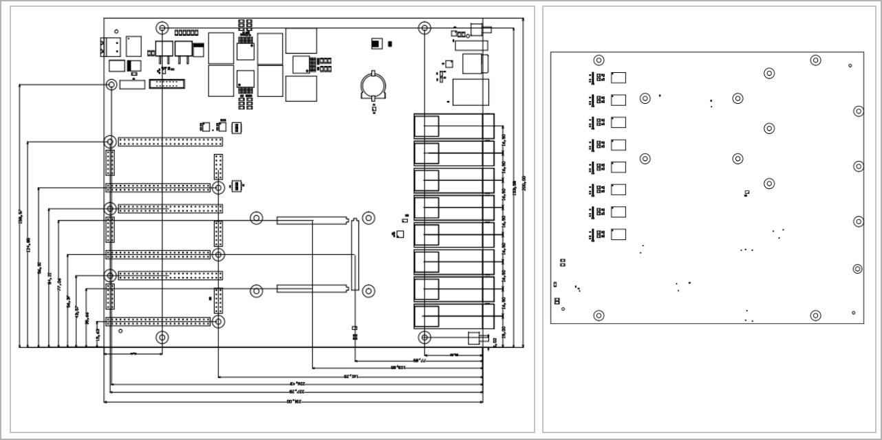 Image Removed Image Removed
|
Currently Offered Variants
...
| anchor | Table_VCP_SO |
|---|
| title | Trenz Electronic Shop Overview |
|---|
| orientation | portrait |
|---|
| sortDirection | ASC |
|---|
| repeatTableHeaders | default |
|---|
| style | |
|---|
| widths | |
|---|
| sortByColumn | 1 |
|---|
| sortEnabled | false |
|---|
| cellHighlighting | true |
|---|
|
| I2C Device | Designator | I2C Address | Notes |
|---|
| I2C Device | U16 | 0x72 |
|
|
IO Expanders
The TEB0745 is equipped with 8 I/O Expanders.
| Scroll Title |
|---|
| anchor | Table_OBP_IOEXP |
|---|
| title | IO Expander Information |
|---|
|
| Scroll Table Layout |
|---|
| orientation | portrait |
|---|
| sortDirection | ASC |
|---|
| repeatTableHeaders | default |
|---|
| style | |
|---|
| widths | |
|---|
| sortByColumn | 1 |
|---|
| sortEnabled | false |
|---|
| cellHighlighting | true |
|---|
|
| Scroll Title |
|---|
| anchor | Table_OBP_SFP |
|---|
| title | SFP Connectors |
|---|
| | Scroll Table Layout |
|---|
| orientation | portrait |
|---|
| sortDirection | ASC |
|---|
| repeatTableHeaders | default |
|---|
| style | |
|---|
| widths | |
|---|
| sortByColumn | 1 |
|---|
| sortEnabled | false |
|---|
| cellHighlighting | true |
|---|
|
| Pin | Connected to | Notes |
|---|
| IO Exp, U18 | IO Exp, U19 | IO Exp, U20 | IO Exp, U21 | IO Exp, U22 | IO Exp, U23 | IO Exp, U24 | IO Exp, U25 |
|---|
| nINT | Not Connected | Not Connected | Not Connected | Not Connected | Not Connected | Not Connected | Not Connected | Not Connected |
| | SCL | I2C Switch, U16 B2B, J2 | I2C Switch, U16 B2B, J2 | I2C Switch, U16 B2B, J2 | I2C Switch, U16 B2B, J2 | I2C Switch, U16 B2B, J2 | I2C Switch, U16 B2B, J2 | I2C Switch, U16 B2B, J2 | I2C Switch, U16 B2B, J2 |
| | SDA | I2C Switch, U16 B2B, J2 | I2C Switch, U16 B2B, J2 | I2C Switch, U16 B2B, J2 | I2C Switch, U16 B2B, J2 | I2C Switch, U16 B2B, J2 | I2C Switch, U16 B2B, J2 | I2C Switch, U16 B2B, J2 | I2C Switch, U16 B2B, J2 |
| | A0 | GND | 3.3V | GND | 3.3V | GND | 3.3V | GND | 3.3V |
| | A1 | GND | GND | 3.3V | 3.3V | GND | GND | 3.3V | 3.3V |
| | A2 | GND | GND | GND | GND | 3.3V | 3.3V | 3.3V | 3.3V |
| | VCC | 3.3V | 3.3V | 3.3V | 3.3V | 3.3V | 3.3V | 3.3V | 3.3V |
| | P0...P7 | SFP+, J4 | SFP+, J6 | SFP+, J8 | SFP+, J10 | SFP+, J13 | SFP+, J15 | SFP+, J18 | SFP+, J20 |
|
|
|
In the following table you can find I2C addresses of I/O Expanders which would be designated by pins A0,A1 and A2.
| Scroll Title |
|---|
| anchor | Table_OBP_IOEXPADD |
|---|
| title | I2C Addresses of I/O Expanders |
|---|
|
| Scroll Table Layout |
|---|
| orientation | portrait |
|---|
| sortDirection | ASC |
|---|
| repeatTableHeaders | default |
|---|
| style | |
|---|
| widths | |
|---|
| sortByColumn | 1 |
|---|
| sortEnabled | false |
|---|
| cellHighlighting | true |
|---|
|
| I2C Device | Designator | I2C Address | Notes |
|---|
| I/O Expander | U18 | 0x20 |
| | U19 | 0x21 |
| | U20 | 0x22 |
| | U21 | 0x23 |
| | U22 | 0x24 |
| | U23 | 0x25 |
| | U24 | 0x26 |
| | U25 | 0x27 |
|
|
Push Buttons
There are two push buttons S2, S3.
| Scroll Title |
|---|
| anchor | Table_OBP_Push_Button |
|---|
| title | On-board push button =s |
|---|
|
| Scroll Table Layout |
|---|
| orientation | portrait |
|---|
| sortDirection | ASC |
|---|
| repeatTableHeaders | default |
|---|
| style | |
|---|
| widths | |
|---|
| sortByColumn | 1 |
|---|
| sortEnabled | false |
|---|
| cellHighlighting | true |
|---|
|
| Designator | Connected to | B2B | Active Level | Note |
|---|
| S3 | USR_BTN | J3-153 | Active high |
| | S2 | RST_IN_N | J2-131 | Active high | General Reset |
|
LEDs
| Scroll Title |
|---|
| anchor | Table_OBP_LED |
|---|
| title | On-board LEDs |
|---|
|
| Scroll Table Layout |
|---|
| orientation | portrait |
|---|
| sortDirection | ASC |
|---|
| repeatTableHeaders | default |
|---|
| style | |
|---|
| widths | |
|---|
| sortByColumn | 1 |
|---|
| sortEnabled | false |
|---|
| cellHighlighting | true |
|---|
|
| Designator | Color | B2B | Connected to | Active Level | Note |
|---|
| D1 | Green | J3-149 | MIO48 | Active High | LED1 | | D5 | Green | J3-151 | MIO49 | Active High | LED2 |
|
Power and Power-On Sequence
| Page properties |
|---|
|
In 'Power and Power-on Sequence' section there are three important digrams which must be drawn: - Power on-sequence
- Power distribution
- Voltage monitoring circuit
|
Power Supply
Power supply with minimum current capability of 2.5 A for system startup is recommended.
Power Consumption
| Scroll Title |
|---|
| anchor | Table_PWR_PC |
|---|
| title | Power Consumption |
|---|
|
| Scroll Table Layout |
|---|
| orientation | portrait |
|---|
| sortDirection | ASC |
|---|
| repeatTableHeaders | default |
|---|
| style | |
|---|
| widths | |
|---|
| sortByColumn | 1 |
|---|
| sortEnabled | false |
|---|
| cellHighlighting | true |
|---|
|
| Power Input Voltage | Typical Current |
|---|
| 24V | TBD* | | VBAT | TBD* |
|
* TBD - To Be Determined
Power Distribution Dependencies
| Scroll Title |
|---|
| anchor | Figure_PWR_PD |
|---|
| title | Power Distribution |
|---|
|
| Scroll Ignore |
|---|
| draw.io Diagram |
|---|
| border | false |
|---|
| viewerToolbar | true |
|---|
| |
|---|
| fitWindow | false |
|---|
| diagramDisplayName | |
|---|
| lbox | true |
|---|
| revision | 10 |
|---|
| diagramName | TEB0745_PWR_PD |
|---|
| simpleViewer | false |
|---|
| width | |
|---|
| links | auto |
|---|
| tbstyle | hidden |
|---|
| diagramWidth | 641 |
|---|
|
|
| Scroll Only |
|---|
Image Added |
|
Power-On Sequence
| Scroll Title |
|---|
| anchor | Figure_PWR_PS |
|---|
| title | Power Sequency |
|---|
|
| Scroll Ignore |
|---|
| draw.io Diagram |
|---|
| border | false |
|---|
| viewerToolbar | true |
|---|
| |
|---|
| fitWindow | false |
|---|
| diagramDisplayName | |
|---|
| lbox | true |
|---|
| revision | 10 |
|---|
| diagramName | TEB0745_PWR_PS |
|---|
| simpleViewer | false |
|---|
| width | 640 |
|---|
| links | auto |
|---|
| tbstyle | hidden |
|---|
| diagramWidth | 630 |
|---|
|
|
| Scroll Only |
|---|
Image Added |
|
Power Rails
| Scroll Title |
|---|
| anchor | Table_PWR_PR |
|---|
| title | Module power rails. |
|---|
|
| Scroll Table Layout |
|---|
| orientation | portrait |
|---|
| sortDirection | ASC |
|---|
| repeatTableHeaders | default |
|---|
| style | |
|---|
| widths | |
|---|
| sortByColumn | 1 |
|---|
| sortEnabled | false |
|---|
| cellHighlighting | true |
|---|
|
| Power Rail Name | B2B Connector JM1 Pin | B2B Connector JM2 Pin | B2B Connector JM3 Pin | Direction | Notes |
|---|
| 3.3V | 147, 149, 151, 153,
155, 157, 159 | 154, 156, 158,160 | - | Output | PL_VIN | | VCCIO12 | 54, 55 | - | - | Output | high range bank I/O voltage | | VCCIO13 | 112, 113 | - | - | Output | high range bank I/O voltage | | VCCIO33 | - | - | 115, 120 | Output | high performance bank I/O voltage | | VCCIO34 | - | 29, 30 | - | Output | high performance bank I/O voltage | | VCCIO35 | - | 87, 88 | - | Output | high performance bank I/O voltage | | VBAT_IN | 146 | - | - | Output | RTC (battery-backed) supply voltage | | PS_1.8V | - | 130 | - | Input | internal 1.8V voltage level (Process System) |
|
Board to Board Connectors
| Page properties |
|---|
|
- This section is optional and only for modules.
use "include page" macro and link to the general B2B connector page of the module series, For example: 6 x 6 SoM LSHM B2B Connectors
|
| Include Page |
|---|
| 5.2 x 7.6 SoM ST5 and SS5 B2B Connectors |
|---|
| 5.2 x 7.6 SoM ST5 and SS5 B2B Connectors |
|---|
|
Technical Specifications
Absolute Maximum Ratings
| Scroll Title |
|---|
| anchor | Table_TS_AMR |
|---|
| title | PS absolute maximum ratings |
|---|
|
| Scroll Table Layout |
|---|
| orientation | portrait |
|---|
| sortDirection | ASC |
|---|
| repeatTableHeaders | default |
|---|
| style | |
|---|
| widths | |
|---|
| sortByColumn | 1 |
|---|
| sortEnabled | false |
|---|
| cellHighlighting | true |
|---|
|
| Symbols | Min | Max | Unit | Note |
|---|
| VIN Supply Voltage | 0 | 24 | V |
| | Storage Temperatur | -25 | +85 | °C |
|
|
Recommended Operating Conditions
Operating temperature range depends also on customer design and cooling solution.
| Scroll Title |
|---|
| anchor | Table_TS_ROC |
|---|
| title | Recommended operating conditions. |
|---|
|
| Scroll Table Layout |
|---|
| orientation | portrait |
|---|
| sortDirection | ASC |
|---|
| repeatTableHeaders | default |
|---|
| style | |
|---|
| widths | |
|---|
| sortByColumn | 1 |
|---|
| sortEnabled | false |
|---|
| cellHighlighting | true |
|---|
|
| Parameter | Min | Max | Units | Reference Document |
|---|
| VIN Supply Voltage | 20 | 25.4 | V | See LTC4365ITS8 Datasheet | | Operating Temperatur | -40 | +85 | °C |
|
|
Physical Dimensions
Module size: 200 mm x 231 mm. Please download the assembly diagram for exact numbers.
Mating height with standard connectors: 3.5 mm.
- PCB thickness: 1.6 mm.
| Page properties |
|---|
|
In 'Physical Dimension' section, top and button view of moduloe must be insterted, information regarding physical dimention can be obtained through webpage for product in Shop.Trenz, (Download> Documents> Assembly part)for every SoM. For Example: for Module TE0728, Physical Dimension information can be captured by snipping tools from the link below: https://www.trenz-electronic.de/fileadmin/docs/Trenz_Electronic/Modules_and_Module_Carriers/5.2x7.6/TE0745/REV02/Documents/AD-TE0745-02-30-1I.PDF
|
| Scroll Title |
|---|
| anchor | Figure_TS_PD |
|---|
| title | Physical dimensions drawing |
|---|
|
| draw.io Diagram |
|---|
| border | false |
|---|
| viewerToolbar | true |
|---|
| |
|---|
| fitWindow | false |
|---|
| diagramDisplayName | |
|---|
| lbox | true |
|---|
| revision | 2 |
|---|
| diagramName | TEB0745_PD |
|---|
| simpleViewer | false |
|---|
| width | |
|---|
| links | auto |
|---|
| tbstyle | hidden |
|---|
| diagramWidth | 641 |
|---|
|
| Scroll Only |
|---|
| scroll-pdf | true |
|---|
| scroll-office | true |
|---|
| scroll-chm | true |
|---|
| scroll-docbook | true |
|---|
| scroll-eclipsehelp | true |
|---|
| scroll-epub | true |
|---|
| scroll-html | true |
|---|
| Image Added |
|
Currently Offered Variants
| Scroll Title |
|---|
| anchor | Table_VCP_SO |
|---|
| title | Trenz Electronic Shop Overview |
|---|
|
| Scroll Table Layout |
|---|
| orientation | portrait |
|---|
| sortDirection | ASC |
|---|
| repeatTableHeaders | default |
|---|
| style | |
|---|
| widths | |
|---|
| sortByColumn | 1 |
|---|
| sortEnabled | false |
|---|
| cellHighlighting | true |
|---|
|
|
Revision History
Hardware Revision History
| Scroll Title |
|---|
| anchor | Table_RH_HRH |
|---|
| title | Hardware Revision History |
|---|
|
| Scroll Table Layout |
|---|
| orientation | portrait |
|---|
| sortDirection | ASC |
|---|
| repeatTableHeaders | default |
|---|
| style | |
|---|
| widths | |
|---|
| sortByColumn | 1 |
|---|
| sortEnabled | false |
|---|
| cellHighlighting | true |
|---|
|
| Date | Revision | Changes | Documentation Link |
|---|
| 2018-12-06 | 02a | - Resistors R14 and R15 was replaced by 953R (was 5K1)
- Resistor R5 was replaced by 5K1, R8 by 953R (was 9K09 and 1K69 respectively)
| REV02-A | | 2018-10-19 | 02 | - U16 I2C expander: address set to 0x72
- U33 EEPROM: address set to 0x51. Added variant to set address 0x52.
- Changed power up sequence: 24V_FUSED -> 3.3V (Module power up) -> 5V -> VCCIO18, VCC_HR_B, 3.3V_SFP
- Fixed PCB patch: U6 pin 18 connected to 5V, pin 19 connected to GND.
- JTAG connector J30 VREF (pin2) and XMOD VIO (pin 6) connected to 3.3V. XMOD IO A, B, E, G connected to module MIO via level translator U8.
- Pull-up for BOOTMODE and PS_SW (DIP switch S1), RST_IN_N and USR_BTN (front panel buttons S2, S3) changed from VCCIO18 to PS_1.8V; JTAG_EN connected to 3.3V via DIP switch (S1).
- Added switch S4 for selecting of output voltage of DCDC U7 (VCC_HR_B, HR banks VCCO)
| REV02 | | 2016-05-25 | 01 | - | REV01 |
|
Hardware revision number can be found on the PCB board together with the module model number separated by the dash.
| Scroll Title |
|---|
| anchor | Figure_RV_HRN |
|---|
| title | Board hardware revision number. |
|---|
|
| Scroll Ignore |
|---|
| draw.io Diagram |
|---|
| border | false |
|---|
| viewerToolbar | true |
|---|
| |
|---|
| fitWindow | false |
|---|
| diagramDisplayName | |
|---|
| lbox | true |
|---|
| revision | 1 |
|---|
| diagramName | TEB0745_RV_HRN |
|---|
| simpleViewer | false |
|---|
| width | 200 |
|---|
| links | auto |
|---|
| tbstyle | hidden |
|---|
| diagramWidth | 129 |
|---|
|
|
| Scroll Only |
|---|
 Image Added Image Added
|
|
Document Change History
| Page properties |
|---|
|
- Note this list must be only updated, if the document is online on public doc!
- It's semi automatically, so do following
Add new row below first Copy "Page Information Macro(date)" Macro-Preview, Metadata Version number, Author Name and description to the empty row. Important Revision number must be the same as the Wiki document revision number Update Metadata = "Page Information Macro (current-version)" Preview+1 and add Author and change description. --> this point is will be deleted on newer pdf export template - Metadata is only used of compatibility of older exports
|
| Scroll Title |
|---|
| anchor | Table_RH_DCH |
|---|
| title | Document change history. |
|---|
|
...
Revision History
Hardware Revision History
...
| anchor | Table_RH_HRH |
|---|
| title | Hardware Revision History |
|---|
...
Document Change History
| Page properties |
|---|
|
- Note this list must be only updated, if the document is online on public doc!
- It's semi automatically, so do following
Add new row below first Copy "Page Information Macro(date)" Macro-Preview, Metadata Version number, Author Name and description to the empty row. Important Revision number must be the same as the Wiki document revision number Update Metadata = "Page Information Macro (current-version)" Preview+1 and add Author and change description. --> this point is will be deleted on newer pdf export template - Metadata is only used of compatibility of older exports
|
...
| anchor | Table_RH_DCH |
|---|
| title | Document change history. |
|---|
...
| Page info |
|---|
| infoType | Modified date |
|---|
| dateFormat | yyyy-MM-dd |
|---|
| type | Flat |
|---|
|
| Page info |
|---|
| infoType | Current version |
|---|
| prefix | v. |
|---|
| type | Flat |
|---|
| showVersions | false |
|---|
|
...
| Page info |
|---|
| infoType | Modified by |
|---|
| type | Flat |
|---|
| showVersions | false |
|---|
|
...
...
--
...
all
...
| Page info |
|---|
| infoType | Modified users |
|---|
| type | Flat |
|---|
| showVersions | false |
|---|
|
...
Disclaimer
...
| Scroll Title |
|---|
| anchor | Table_OBP_EEP |
|---|
| title | I2C EEPROM interface MIOs and pins |
|---|
|
| Scroll Table Layout |
|---|
| orientation | portrait |
|---|
| sortDirection | ASC |
|---|
| repeatTableHeaders | default |
|---|
| style | |
|---|
| widths | |
|---|
| sortByColumn | 1 |
|---|
| sortEnabled | false |
|---|
| cellHighlighting | true |
|---|
|
|
| MIO Pin | Schematic | B2B | Notes |
|---|
MIO10 | I2C_SCL | J2-119 | MIO11 | I2C_SDA | J2-121 | | Date | Revision | Contributor | Description |
|---|
| Page info |
|---|
| infoType | Modified date |
|---|
| dateFormat | yyyy-MM-dd |
|---|
| type | Flat |
|---|
|
| | Page info |
|---|
| infoType | Current version |
|---|
| prefix | v. |
|---|
| type | Flat |
|---|
| showVersions | false |
|---|
|
| | Page info |
|---|
| infoType | Modified by |
|---|
| type | Flat |
|---|
| showVersions | false |
|---|
|
| |
| 2020-09-01 | v.135 | John Hartfiel | - Correction power sequencing picture
|
| 2019-12-08 | v.134 | Pedram Babakhani | - Technical Specifications Update
|
-- | all | | Page info |
|---|
| infoType | Modified users |
|---|
| type | Flat |
|---|
| showVersions | false |
|---|
|
| |
Disclaimer
| Include Page |
|---|
| IN:Legal Notices |
|---|
| IN:Legal Notices |
|---|
|
| draw.io Diagram |
|---|
| border | false |
|---|
| viewerToolbar | true |
|---|
| fitWindow | false |
|---|
diagramDisplayName | | lbox | true |
|---|
| revision | 6 |
|---|
| diagramName | TEB0745_PWR_PD |
|---|
| simpleViewer | false |
|---|
width | | links | auto |
|---|
| tbstyle | hidden |
|---|
| diagramWidth | 641 |
|---|
|