...
- FPGA: Xilinx Artix 7 (XC7A100T)
- Package: FGG484 (Compatible with
- Speed: -1 (Slowest)
- Temperature: Industrial Grade (–40°C to +100°C)
- RAM/Storage:
- 1x NOR SPI FLASH (128M x 4)
- 1x EEPROM (16K x 8)
- On Board:
- 4x Deserializer IC (3.12 Gbps)
- 4x I2C and SMBus I/O Expander
- 1x Programable Clock Generator
- 1x Clock Generator
- Interface:
- 2x VITA 57 SEAM/SEAF Series
- 4x Coaxial Connectors
- Power:
- 4x Voltage Regulators
- 3.3 Supply Voltage
- Dimension:
Block Diagram
| Page properties |
|---|
|
add drawIO object here.
|
...
| Scroll Title |
|---|
| anchor | Figure_OV_BD |
|---|
| title | TEF0003 block diagram |
|---|
|
| Scroll Ignore |
|---|
| draw.io Diagram |
|---|
| border | false |
|---|
| viewerToolbar | true |
|---|
| |
|---|
| fitWindow | false |
|---|
| diagramDisplayName | |
|---|
| lbox | true |
|---|
| revision | 1012 |
|---|
| diagramName | TEF0003_OV_BD |
|---|
| simpleViewer | false |
|---|
| width | |
|---|
| links | auto |
|---|
| tbstyle | hidden |
|---|
| diagramWidth | 641 |
|---|
|
|
| Scroll Only |
|---|
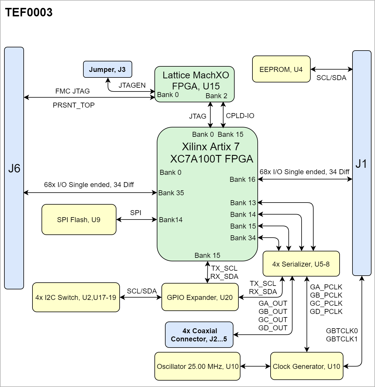 Image Modified Image Modified
|
|
Main Components
...
| Scroll Title |
|---|
| anchor | Figure_OV_MC |
|---|
| title | TEF0003 main components |
|---|
|
| Scroll Ignore |
|---|
| draw.io Diagram |
|---|
| border | false |
|---|
| viewerToolbar | true |
|---|
| |
|---|
| fitWindow | false |
|---|
| diagramDisplayName | |
|---|
| lbox | true |
|---|
| revision | 7 |
|---|
| diagramName | TEF0003_OV_MC |
|---|
| simpleViewer | false |
|---|
| width | |
|---|
| links | auto |
|---|
| tbstyle | hidden |
|---|
| diagramWidth | 641 |
|---|
|
|
| Scroll Only |
|---|
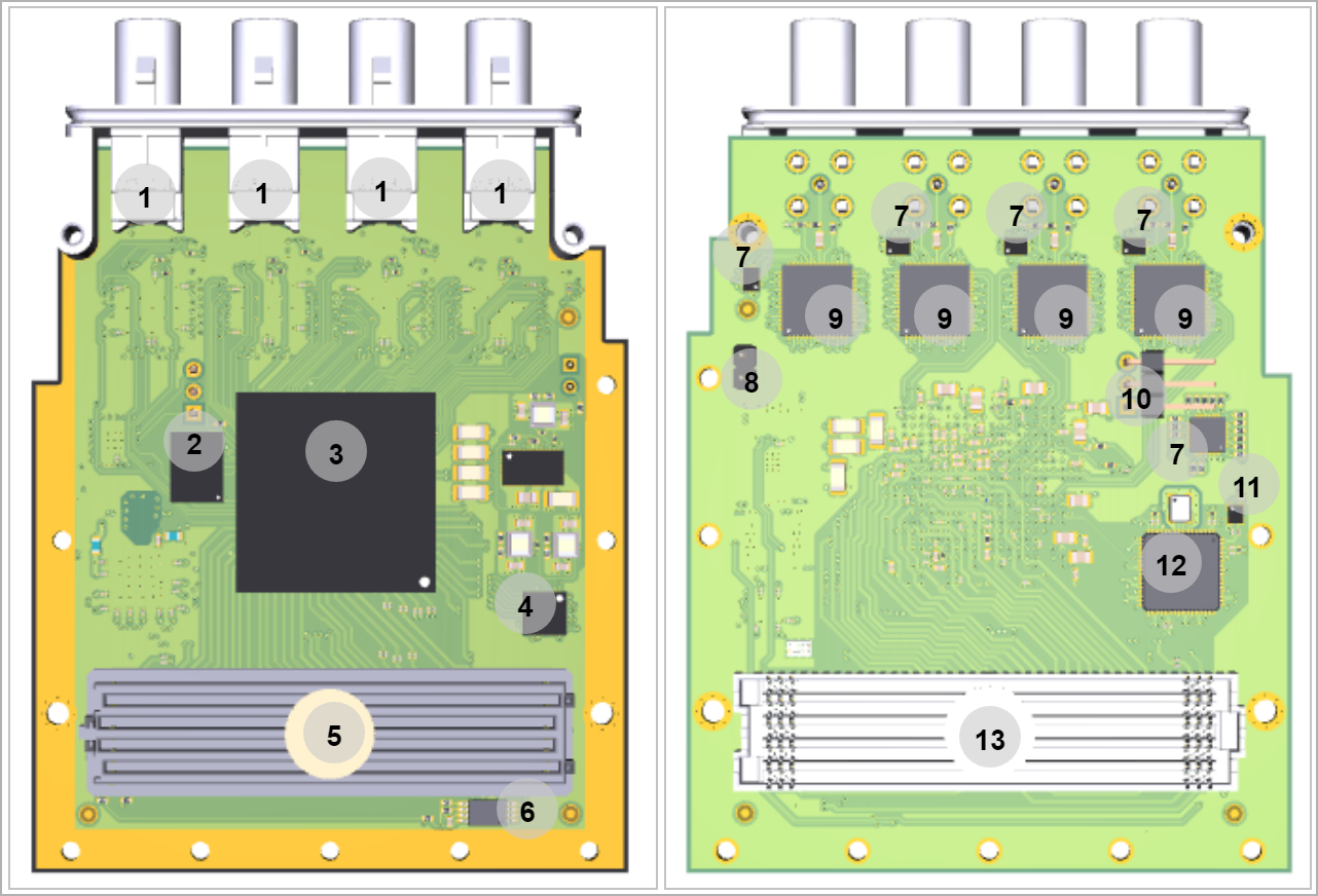 Image Modified Image Modified
|
|
- Coaxial Connectors, J2-5
- SPI Flash, U9
- Xilinx Artix 7 FPGA, U1
- Lattice MachXO FPGA, U15
- FMC Adapter, J1
- EEPROM, U4
- I2C Switches, U2, U17-20
- Jumper, J7
- Serializer, U5-8
- Connector Header, J8
- Oscillator 25MHz, U11
- Programmable Clock Generator, U10
- FMC Adapter, J6
...
| Scroll Title |
|---|
| anchor | Table_OV_RST |
|---|
| title | Reset Process. |
|---|
|
| Scroll Table Layout |
|---|
| orientation | portrait |
|---|
| sortDirection | ASC |
|---|
| repeatTableHeaders | default |
|---|
| sortByColumn | 1 |
|---|
| sortEnabled | false |
|---|
| cellHighlighting | true |
|---|
|
Signal | Description | Note |
|---|
PRSNT_TOP | Lattice MachXO Configuration Pin |
| | PROG_B | Artix 7 Configuration Pin | Connected Pulled up to 1.8 |
|
Signals, Interfaces and Pins
...
| Scroll Title |
|---|
| anchor | Table_SIP_FMC |
|---|
| title | General PL I/O to FMC Connectors information |
|---|
|
| Scroll Table Layout |
|---|
| orientation | portrait |
|---|
| sortDirection | ASC |
|---|
| repeatTableHeaders | default |
|---|
| sortByColumn | 1 |
|---|
| sortEnabled | false |
|---|
| cellHighlighting | true |
|---|
|
| FPGA | FPGA Bank | Connector Designator | I/O Signal Count | Voltage Level | Notes |
|---|
| Artix 7, U1 | 16 | J1B | 68 Single Ended, 34 Differential | 1.8V |
| | 35 | J6B | 68 Single Ended, 34 Differential | 1.8V |
| | Lattice MachXO, U | 0 | J1F | 4 Single Ended | 3.3V | CPLD | | 0 | J6F | 4 Single Ended | 3.3V | CPLD |
|
...
Coaxial Connectors
The Lattice MachXO (U15) is available to meet the requirement of a CPLD, JTAG access to the MachXO is available through FMC Adapter J6. JTAG access to the Artix 7(U1) is available via MachXO, Bank 2.
| Scroll Title |
|---|
| anchor | Table_SIP_CPLDJTGCoaxial |
|---|
| title | CPLD JTAG pins connectionCoaxial Connectors information |
|---|
|
| Scroll Table Layout |
|---|
| orientation | portrait |
|---|
| sortDirection | ASC |
|---|
| repeatTableHeaders | default |
|---|
| sortByColumn | 1 |
|---|
| sortEnabled | false |
|---|
| cellHighlighting | true |
|---|
|
JTAG Signal| Designator | Schematic | Connected to | Notes |
|---|
| J2 | GA_OUT | Serializer, U5 |
| | J3 | GB_OUT | Serializer, U6 |
| | J4 | GC_OUT | Serializer, U7 |
| | J5 | GD_OUT | Serializer, U8 |
|
|
JTAG Interface
The Lattice MachXO (U15) is available to meet the requirement of a CPLD, JTAG access to the MachXO is available through FMC Adapter J6. JTAG access to the Artix 7(U1) is available via MachXO, Bank 2.
| Scroll Title |
|---|
| anchor | Table_SIP_CPLDJTG |
|---|
| title | CPLD JTAG pins connection |
|---|
|
| Scroll Table Layout |
|---|
| orientation | portrait |
|---|
| sortDirection | ASC |
|---|
| repeatTableHeaders | default |
|---|
| sortByColumn | 1 |
|---|
| sortEnabled | false |
|---|
| cellHighlighting | true |
|---|
|
JTAG Signal | B2B Connector | Notes |
|---|
| FMC |
B2B Connector | FMC| _TMS | J6F-TCK |
| | FMC_TDI_TOP | J6F-J1-TDI |
| | FMC_TDO_TOP | J6F-TDO |
| | FMC_TCK | J6F-TCK |
| | JTAGEN |
J7
|
| Scroll Title |
|---|
| anchor | Table_SIP_JTG |
|---|
| title | JTAG pins connection |
|---|
|
| Scroll Table Layout |
|---|
| orientation | portrait |
|---|
| sortDirection | ASC |
|---|
| repeatTableHeaders | default |
|---|
| sortByColumn | 1 |
|---|
| sortEnabled | false |
|---|
| cellHighlighting | true |
|---|
|
JTAG Signal | Connected to | Note |
|---|
| TMS | Lattice MachXO, U15 BankArtix 7 FPGA, U1 | Bank 2 Bank 0 | | TDI | Lattice MachXO, U15 Artix 7 FPGA, U1 | Bank 2 Bank 0 | | TDO | Lattice MachXO, U15 Artix 7 FPGA, U1 | Bank 2 Bank 0 | | TCK | Lattice MachXO, U15 Artix 7 FPGA, U1 | Bank 2 Bank 0 | | INIT | Artix 7 FPGA, U1 | Connected Pulled up to 1.8 |
|
On-board Peripherals
...
| Scroll Title |
|---|
| anchor | Table_OBP |
|---|
| title | On board peripherals |
|---|
|
| Scroll Table Layout |
|---|
| orientation | portrait |
|---|
| sortDirection | ASC |
|---|
| repeatTableHeaders | default |
|---|
| sortByColumn | 1 |
|---|
| sortEnabled | false |
|---|
| cellHighlighting | true |
|---|
|
|
Quad SPI Flash Memory
| Page properties |
|---|
|
Notes : Minimum and Maximum density of quad SPI flash must be mentioned for other assembly options. |
...
| Scroll Title |
|---|
| anchor | Table_OBP_EEP |
|---|
| title | I2C EEPROM interface MIOs and pins |
|---|
|
| Scroll Table Layout |
|---|
| orientation | portrait |
|---|
| sortDirection | ASC |
|---|
| repeatTableHeaders | default |
|---|
| sortByColumn | 1 |
|---|
| sortEnabled | false |
|---|
| cellHighlighting | true |
|---|
|
| U4 Pin | FMC Pcam Adapter | Schematic |
|---|
U4 PinNotesSCLSDA | J1F-GA0 | GA0 | A0 | |
| | A0 | J1F-GA0 | GA0 |
| | A1 | J1F-GA1 | GA1 |
| | A2 | - | - | Pulled Low | | WP | - | - | Pulled Low |
J1F-GA1 | GA1 | A1
|
| Scroll Title |
|---|
| anchor | Table_OBP_I2C_EEPROM |
|---|
| title | I2C address for EEPROM |
|---|
|
| Scroll Table Layout |
|---|
| orientation | portrait |
|---|
| sortDirection | ASC |
|---|
| repeatTableHeaders | default |
|---|
| sortByColumn | 1 |
|---|
| sortEnabled | false |
|---|
| cellHighlighting | true |
|---|
|
| I2C Address | Designator | Notes |
|---|
0x50| 0xA0 | U4 | Write operations are enabled |
|
Clock Sources
| Scroll Title |
|---|
| anchor | Table_OBP_CLK |
|---|
| title | Osillators |
|---|
|
| Scroll Table Layout |
|---|
| orientation | portrait |
|---|
| sortDirection | ASC |
|---|
| repeatTableHeaders | default |
|---|
| sortByColumn | 1 |
|---|
| sortEnabled | false |
|---|
| cellHighlighting | true |
|---|
|
| Designator | Description | Frequency | Note |
|---|
| U4U11 | Oscillator | 25 MHz.00 MHz |
| | U10 | Programmable Clock Generator | Variable |
|
|
...
There is a Silicon Labs I2C programmable clock generator on-board (U10) in order to generate reference clocks for the module. Programming can be done using I2C via PIN header J8. The I2C Address is 0x69.
| Scroll Title |
|---|
| anchor | Table_OBP_PCLK |
|---|
| title | Programmable Clock Generator Inputs and Outputs |
|---|
|
| Scroll Table Layout |
|---|
| orientation | portrait |
|---|
| sortDirection | ASC |
|---|
| repeatTableHeaders | default |
|---|
| sortByColumn | 1 |
|---|
| sortEnabled | false |
|---|
| cellHighlighting | true |
|---|
|
Si5345A Pin
| Signal Name / Description
| Connected To | Direction | Note |
|---|
IN0 | Reference input clock. | U11 | Input | 25.00 MHz oscillator, SiT8008BI | | IN1 | FMCT_GBTCLK0 | J6E | Input | FMC Pcam Adapter | | IN2 | FMCT_GBTCLK1 | J6E | Input | FMC Pcam Adapter | | IN3 | FMCT_CLK0 | J6E | Input | FMC Pcam Adapter | XAXB | - | GND | Input | 54.0000 00 MHz XTAL CX3225SB | | SCLK | PLL_SCL | J8, U20 | Input | EEPROM Programming | | SDA | PLL_SDA | J8, U20 | Input | EEPROM Programming | | OUT0 | GA_PCLK | U5/U1 | Output | FPGA bank 15 | | OUT1 | GB_PCLK | U6/U1 | Output | FPGA bank 15 | | OUT2 | GC_PCLK | U7/U1 | Output | FPGA bank 15 | | OUT3 | GD_PCLK | U8/U1 | Output | FPGA bank 15 | | OUT4 | CLK4_P | U1H | Output |
| | OUT5 | GBTCLK0 | J1E/J6E | Output |
| | OUT6 | GBTCLK1 | J1E/J6E | Output |
| | OUT7 | GBTCLK0 | J1E | Output |
| | OUT8/OUT9 | CLK8/CLK9 | Pulled low | Output |
|
|
...
| Scroll Title |
|---|
| anchor | Table_PWR_PC |
|---|
| title | Power Consumption |
|---|
|
| Scroll Table Layout |
|---|
| orientation | portrait |
|---|
| sortDirection | ASC |
|---|
| repeatTableHeaders | default |
|---|
| sortByColumn | 1 |
|---|
| sortEnabled | false |
|---|
| cellHighlighting | true |
|---|
|
| Power Input Pin | Typical Current |
|---|
| VIN3P3V | TBD* |
|
* TBD - To Be Determined
...
| Scroll Title |
|---|
| anchor | Figure_PWR_PD |
|---|
| title | Power Distribution |
|---|
|
| Scroll Ignore |
|---|
| draw.io Diagram |
|---|
| border | false |
|---|
| viewerToolbar | true |
|---|
| |
|---|
| fitWindow | false |
|---|
| diagramDisplayName | |
|---|
| lbox | true |
|---|
| revision | 57 |
|---|
| diagramName | TEF0003_PWR_PD |
|---|
| simpleViewer | false |
|---|
| width | |
|---|
| links | auto |
|---|
| tbstyle | hidden |
|---|
| diagramWidth | 641 |
|---|
|
|
| Scroll Only |
|---|
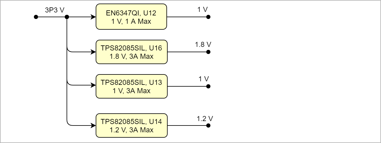 Image Modified Image Modified
|
|
Power-On Sequence
| Scroll Title |
|---|
| anchor | Figure_PWR_PS |
|---|
| title | Power Sequency |
|---|
|
| Scroll Ignore |
|---|
| draw.io Diagram |
|---|
| border | false |
|---|
| viewerToolbar | true |
|---|
| |
|---|
| fitWindow | false |
|---|
| diagramDisplayName | |
|---|
| lbox | true |
|---|
| revision | 2 |
|---|
| diagramName | TEF0003_PWR_PS |
|---|
| simpleViewer | false |
|---|
| width | |
|---|
| links | auto |
|---|
| tbstyle | hidden |
|---|
| diagramWidth | 641 |
|---|
|
|
| Scroll Only |
|---|
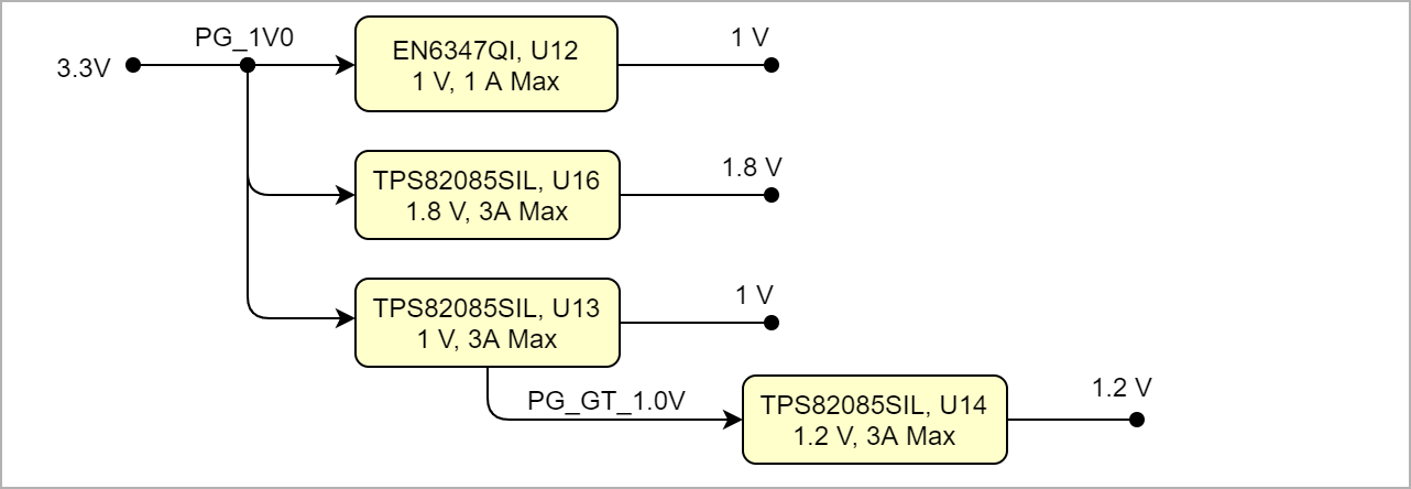 Image Modified Image Modified
|
|
Power Rails
...
| Scroll Title |
|---|
| anchor | Table_TS_AMR |
|---|
| title | PS absolute maximum ratings |
|---|
|
| Scroll Table Layout |
|---|
| orientation | portrait |
|---|
| sortDirection | ASC |
|---|
| repeatTableHeaders | default |
|---|
| sortByColumn | 1 |
|---|
| sortEnabled | false |
|---|
| cellHighlighting | true |
|---|
|
| Symbols | Description | Min | Max | Unit |
|---|
| 12V3P3V | Input Supply Voltage | -12120.5 | 3.75 | V | | T_STG | Storage Temperature | -40 | 85 | °C |
|
Recommended Operating Conditions
...
| Scroll Title |
|---|
| anchor | Table_TS_ROC |
|---|
| title | Recommended operating conditions. |
|---|
|
| Scroll Table Layout |
|---|
| orientation | portrait |
|---|
| sortDirection | ASC |
|---|
| repeatTableHeaders | default |
|---|
| sortByColumn | 1 |
|---|
| sortEnabled | false |
|---|
| cellHighlighting | true |
|---|
|
| Parameter | Min | Max | Units | Reference Document |
|---|
12V12 | 12| 2.375 | 3.465 | V |
| | T_OPR | -40 | 85 | °C | See MT25QU512ABB8E12-0SIT (U9) datasheet. |
|
Physical Dimensions
Module size: 84 mm × 65 mm. Please download the assembly diagram for exact numbers.
Mating height with standard connectors: 10 mm.
...
| Scroll Title |
|---|
| anchor | Figure_TS_PD |
|---|
| title | Physical Dimension |
|---|
|
| draw.io Diagram |
|---|
| border | false |
|---|
| viewerToolbar | true |
|---|
| |
|---|
| fitWindow | false |
|---|
| diagramDisplayName | |
|---|
| lbox | true |
|---|
| revision | 25 |
|---|
| diagramName | TEF0003_TS_PD |
|---|
| aspect | 5e705185-5827-752c-089d-756568e6698b |
|---|
| simpleViewer | false |
|---|
| width | 639 |
|---|
| aspectHash | 7695f7bc00c98da1082cb1c11a0a6258edf875fc |
|---|
| links | auto |
|---|
| tbstyle | hidden |
|---|
| diagramWidth | 436 |
|---|
|
| Scroll Only |
|---|
| scroll-pdf | true |
|---|
| scroll-office | true |
|---|
| scroll-chm | true |
|---|
| scroll-docbook | true |
|---|
| scroll-eclipsehelp | true |
|---|
| scroll-epub | true |
|---|
| scroll-html | true |
|---|
| 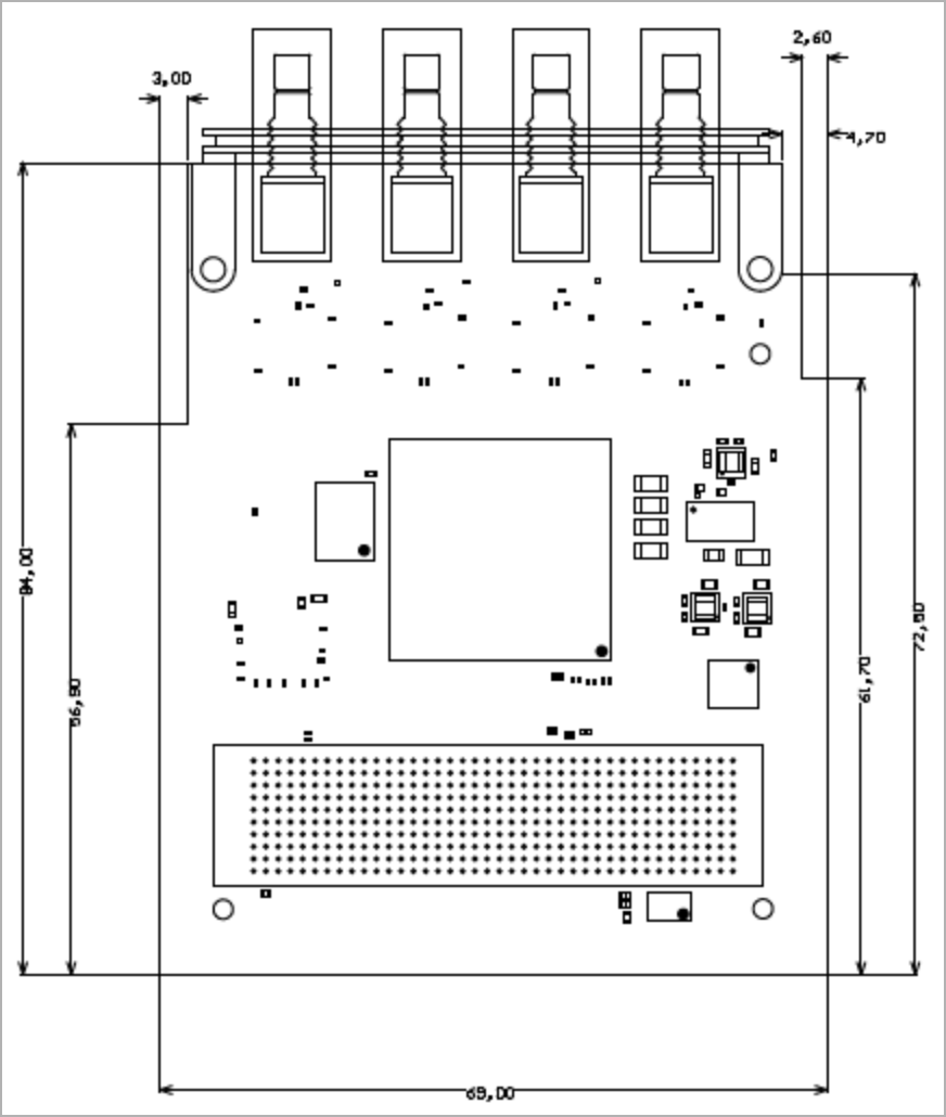 Image Modified Image Modified
|
|
Currently Offered Variants
...
| Scroll Title |
|---|
| anchor | Table_RH_HRH |
|---|
| title | Hardware Revision History |
|---|
|
| Scroll Table Layout |
|---|
| orientation | portrait |
|---|
| sortDirection | ASC |
|---|
| repeatTableHeaders | default |
|---|
| sortByColumn | 1 |
|---|
| sortEnabled | false |
|---|
| cellHighlighting | true |
|---|
|
| Date | Revision | Changes | Documentation Link |
|---|
| 2017-06-27 | REV01 | Initial Release | REV01 |
|
Hardware revision number can be found on the PCB board together with the module model number separated by the dash.
...