| Page properties |
|---|
|
- Module: TRM Name always "TE Series Name" +TRM
Example: "TE0728 TRM"
Template Change history: | Date | Version | Changes | Author |
|---|
| 4.1 | | ED |
| 4.0 | - Rework for smaller TRM which can be generated faster
- Reduce Signal Interfaces Pin
- Reduce On Board Perihery
- Reduce Power
- Move Configuration Signals from Overview to own section
| JH |
| 3.12 | - Version History
- changed from list to table
- all
- changed title-alignment for tables from left to center
| ma |
| 3.11 | - update "Recommended Operating Conditions" section
|
|
| 3.1 | - New general notes for temperature range to "Recommended Operating Conditions"
|
|
| 3.02 | - add again fix table of content with workaround to use it for pdf and wiki
- Export Link for key features examples
- Notes for different Types (with and without Main FPGA)
- Export Link for Signals, Interfaces and Pins examples
- Notes for different Types (Modul, Modul Hypride, Evalboard, Carrier)
|
|
| 3.01 | - remove fix table of content and page layout ( split page layout make trouble with pdf export)
- changed and add note to signal and interfaces, to on board periphery section
- ...(not finished)
|
|
| 3.00 | - → separation of Carrier/Module and evaluation kit TRM
|
|
| 2.15 | - add excerpt macro to key features
|
|
| 2.14 | - add fix table of content
- add table size as macro
|
|
|
| Page properties |
|---|
|
Important General Note:
|
| Page properties |
|---|
|
----------------------------------------------------------------------- |
| Page properties |
|---|
|
Note for Download Link of the Scroll ignore macro: |
Overview
The Trenz Electronic TE0817 is an industrial grade MPSoC SOM SoM integrating a Xilinx an AMD Zynq UltraScale+ MPSoC, DDR4 SDRAM with 64-Bit width data bus connection, SPI Boot Flash memory for configuration and operation, transceivers and powerful switch-mode power supplies for all on-board voltages. A large number of configurable I/Os is provided via rugged high-speed stacking connections in a compact 5.2 cm x 7.6 cm form factor.
Refer to http://trenz.org/te0817-info for the current online version of this manual and other available documentation.
Key Features
| Excerpt |
|---|
- SoC
- Device: ZU4 / ZU5 / ZU7 1)
- Engine: CG / EG / EV 1)
- Speedgrade: -1 / -2 / -3 1)
- Temperature Range: Extended / Industrial 1)
- Package: FBVB900
- RAM/Storage
- 4 GByte DDR4 SDRAM 2)
- 2 x 64 MByte Serial Flash 3)
- EEPROM with MAC address
- On Board
- Interface
- 4 x B2B Connector (ADM6)
up to 204 PL IO up to 65 PS MIO - 4 GTR
- 16 GTH
- I2C, JTAG
- Power
- 3.3 V power Power supply via B2B Connector needed 4).
- Dimension
- Notes
1) Please, take care of the possible assembly options. Furthermore, check whether the power supply is powerful enough for your FPGA design.
2) Up to 32 8 GByte are possible with a maximum bandwidth of 2400 MBit/s.
3) Please, take care of the possible assembly options.
4) Dependant on the assembly option a higher input voltage may be possible.
|
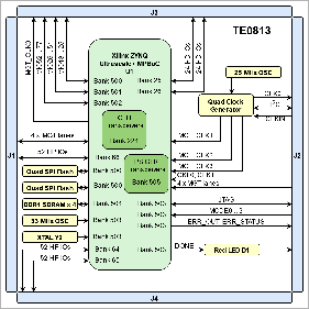
Block Diagram
| Page properties |
|---|
|
add drawIO object in Scroll Ignore section and add reference image in Scroll Only.
| Note |
|---|
Title (not anchor) of all Scroll Title such as DrawIOs and Tables should be changed according to the Module name. Example: TE0812 Block Diagram |
| Note |
|---|
All created DrawIOs should be named according to the Module name: Example: DrawIO of TE0812 Block Diagram should be named TE0812_OV_BD |
|
| Scroll Title |
|---|
| anchor | Figure_OV_BD |
|---|
| title-alignment | center |
|---|
| title | TE0813 TE0817 block diagram |
|---|
|
| Scroll Ignore |
|---|
| draw.io Diagram |
|---|
| border | true |
|---|
| |
|---|
| diagramName | TE0817_OV_BD |
|---|
| simpleViewer | falsetrue |
|---|
| width | |
|---|
| links | auto |
|---|
| tbstyle | top |
|---|
| diagramDisplayName | |
|---|
| lbox | true |
|---|
| diagramWidth | 641642 |
|---|
| revision | 35 |
|---|
|
|
| Scroll Only |
|---|
|
|
Main Components
| Page properties |
|---|
|
Notes : - Picture of the PCB (top and bottom side) with labels of important components
- Add List below
|
| Scroll Title |
|---|
| anchor | Figure_OV_MC |
|---|
| title-alignment | center |
|---|
| title | TE0813 TE0817 main components |
|---|
|
| Scroll Ignore |
|---|
| draw.io Diagram |
|---|
| border | true |
|---|
| |
|---|
| diagramName | Figure_OV_MC |
|---|
| simpleViewer | falsetrue |
|---|
| width | |
|---|
| links | auto |
|---|
| tbstyle | top |
|---|
| diagramDisplayName | |
|---|
| lbox | true |
|---|
| diagramWidth | 722721 |
|---|
| revision | 37 |
|---|
|
|
| Scroll Only |
|---|
 Image Removed Image Removed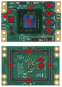 Image Added Image Added
|
|
- SoC, U1
- DDR4, U2, U3, U9, U12
- Quad SPI Flash, U7, U17
- Connector, J1, J2, J3, J4
- EEPROM, U11
- Clock Generator, U5
- Oscillator, U25, U32Power Supply, U4, U6, U8, U10, U13 ... U15, U18 ... U24, U26 ... U31, U34, U38
Initial Delivery State
| Page properties |
|---|
|
| Note |
|---|
Only components like EEPROM, QSPI flash can be initialized by default at manufacture. If there is no components which might have initial data ( possible on carrier) you must keep the table empty |
|
| Scroll Title |
|---|
| anchor | Table_OV_IDS |
|---|
| title-alignment | center |
|---|
| title | Initial delivery state of programmable devices on the module |
|---|
|
| Scroll Table Layout |
|---|
| orientation | portrait |
|---|
| sortDirection | ASC |
|---|
| repeatTableHeaders | default |
|---|
| style | |
|---|
| widths | |
|---|
| sortByColumn | 1 |
|---|
| sortEnabled | false |
|---|
| cellHighlighting | true |
|---|
|
Storage device name | Content | Notes |
|---|
| DDR4 SDRAM | not programmed |
| | Quad SPI Flash | not programmed |
| | EEPROM | not programmed besides factory programmed MAC address |
| | Programmable Clock Generator | not programmed |
|
|
Signals, Interfaces and Pins
Connectors
| Scroll Title |
|---|
| anchor | Table_SIP_C |
|---|
| title-alignment | center |
|---|
| title | Board Connectors |
|---|
|
| Scroll Table Layout |
|---|
| orientation | portrait |
|---|
| sortDirection | ASC |
|---|
| repeatTableHeaders | default |
|---|
| style | |
|---|
| widths | |
|---|
| sortByColumn | 1 |
|---|
| sortEnabled | false |
|---|
| cellHighlighting | true |
|---|
|
| Connector Type | Designator | Interface | IO CNT 1) | Notes |
|---|
| B2B | JM1J1 | MGT PL | 4 12 x MGT (RX/TX) |
| | B2B | JM1J1 | HP | 52 SE / 24 DIFF |
| | B2B | JM2J2 | MGT PS | 2 x MGT CLK |
| | B2B | J2 | CLK | DIFF CLK |
| | B2B | J2 | MGT PL | 4 x MGT (RX/TX) |
| | B2B | JM2J2 | MGT PS | 4 x MGT (RX/TX) |
| | B2B | JM2J2 | CFG | JTAG |
| | B2B | JM2J2 | CFG | MODE |
| | B2B | JM3J3 | HD | 48 SE / 24 DIFF |
| | B2B | JM3J3 | MGT PL | 3 x MGT CLK |
| | B2B | J3 | CLK | DIFF CLK |
| | B2B | JM3J3 | MIO | 65 GPIO |
| | B2B | JM4J4 | HP | 104 SE / 48 DIFF |
|
1) IO CNT depends on assembly variant. E.g. the MGTs are not available for all FPGAs |
Test Points
| Page properties |
|---|
|
you must fill the table below with group of Test Point which are indicated as TP in a schematic. If there is no Test Point remarked in the schematic, delet the Test Point section. Example: | Test Point | Signal | Notes1) |
|---|
| TP1 | PWR_PL_OK |
|
1) Direction: - IN: Input from the point of view of this board.
- OUT: Output from the point of view of this board.
|
| Scroll Title |
|---|
| anchor | Table_SIP_TPs |
|---|
| title-alignment | center |
|---|
| title | Test Points Information |
|---|
|
| Scroll Table Layout |
|---|
| orientation | portrait |
|---|
| sortDirection | ASC |
|---|
| repeatTableHeaders | default |
|---|
| style | |
|---|
| widths | |
|---|
| sortByColumn | 1 |
|---|
| sortEnabled | false |
|---|
| cellHighlighting | true |
|---|
|
| Test | PointPoint 1) | Signal | Notes1Notes 2) |
|---|
| TP1 | PLL_SCL | pulled-up to | PSSI_PLL_1V8 | | TP2 | PLL_SDA | pulled-up to | PSSI_PLL_1V8 | | TP3 | DDR4-TEN | pulled-down to GND | | TP4 | VTT |
| | TP5 | GND |
| | TP6 | PL_1V8TCK |
| | TP7 | GNDTDI |
| | TP8 | GNDTDO |
| | TP9 | PL_VCCINT_IOTMS |
| | TP10 | GNDLP_0V85 |
| | TP11 | PLFP_ | VCCINT0V85 |
| | TP12 | PL_ | VCU_0V9VCCINT |
| | TP13 | FPPS_0V85PLL |
| | TP14 | PS_GT_1V81V0 |
| | TP15GND | FP_0V85 |
| | TP16 | DDR_2V5 |
| | TP17 | DCDC_2V0 |
| | TP18 | DDR_PLL | TP18
| | TP19 | DDRPS_GT_ | 1V21V0 |
| | TP20 | MGTAVTTPL_VCU |
| | TP21 | VTTPS_AUX |
| | TP22 | PLPS_ | GT_1V05AVCC |
| | TP23 | VREFAVTT |
| | TP24 | MGTVCCAUXAUX_R |
| | TP25 | | AVTT_R |
| | TP26 | AVCC_R | MGTAVCC |
| | TP27 | PS_PLL |
| | TP28 | PS_AVTT |
| | TP29 | LPPS_ | 0V85AUX |
| | TP30 | PS_ | AUXAVCC |
| | TP31 | PSLP_ | AVCC0V85 |
| TP34| TP32 | POR_B | pulled-up to PS_1V8 |
1) Direction: - IN: Input from the point of view of this board.
- OUT: Output from the point of view of this board.
|
On-board Peripherals
| Page properties |
|---|
|
Notes :
In the on-board peripheral table "chip/Interface" must be linked to the corresponding chapter or subsection by assigning advance link using: #NameOfTheSection
Example:
| GND |
| | TP33 | PS_AVTT |
| | TP34 | DDR_PLL |
| | TP35 | DDR_2V5 |
| | TP36 | VREFA |
| | TP37 | VREFA |
| | TP38 | 3.3VIN |
| | TP39 | LP_DCDC |
| | TP40 | PL_VCCINT |
| | TP41 | DCDCIN |
| | TP42 | DCDC_2V0 |
| | TP43 | PL_DCIN |
| | TP44 | PL_GT_1V45 |
| | TP45 | PL_GT_1V45 |
| | TP46 | GT_DCDC |
| | TP47 | PL_GT_1V15 |
| | TP48 | PL_GT_1V15 |
| | TP49 | PLL_3V3 |
| | TP50 | AUX_R |
| | TP51 | PSBATT |
| | TP52 | AVCC_R |
| | TP53 | AVTT_R |
| | TP54 | VCCO_47 |
| | TP55 | PL_VCU |
| | TP56 | VCCO_48 |
| | TP57 | 1V8_REFIN |
| | TP58 | 1V8_REFIN |
| | TP59 | VCCO_64 |
| | TP60 | 1V25_REF |
| | TP61 | 1V25_REF |
| | TP62 | VCCO_65 |
| | TP63 | VCCO_66 |
| | TP64 | PLL_VDDA |
| | TP65 | PLL_VDDA |
| | TP66 | PLL_VDD |
| | TP67 | PLL_VDD |
| | TP68 | PS_1V8 |
| | TP69 | PL_1V8 |
| | TP70 | SI_PLL_1V8 |
| | TP71 | SI_PLL_1V8 |
| | TP72 | DDR4_1V2 |
|
1) Test points depend on revision: Not all testpoints are available for all revisions. 2) Direction: - IN: Input from the point of view of this board.
- OUT: Output from the point of view of this board.
|
On-board Peripherals
| Chip/Interface | Designator | Connected To | Notes |
|---|
| ETH PHY | U10 | | Gigabit ETH PHY |
| Scroll Title |
|---|
| anchor | Table_OBP |
|---|
| title-alignment | center |
|---|
| title | On board peripherals |
|---|
|
| Scroll Table Layout |
|---|
| orientation | portrait |
|---|
| sortDirection | ASC |
|---|
| repeatTableHeaders | default |
|---|
style | widths | | sortByColumn | 1 |
|---|
| sortEnabled | false |
|---|
| cellHighlighting | true |
|---|
| Chip/Interface | Designator | Connected To | Notes |
|---|
DDR4 SDRAM | U2, U3, U9, U12 | SoC - PS | Quad SPI Flash | U7, U17 | SoC - PS | Booting. |
EEPROM | U28 | B2B - J2 | Clock Generator | U5 | SoC, B2B | Oscillator | U6 | Clock Generator | 25 MHz |
Oscillator | U32 | SoC | 33.333333 MHz |
Configuration and System Control Signals
| Anchor |
|---|
Configuration and System Control Signals | Configuration and System Control Signals | | Page properties |
|---|
|
Notes : In the on-board peripheral table "chip/Interface" must be linked to the corresponding chapter or subsection by assigning advance link using: #NameOfTheSection Example: | Chip/Interface | Designator | Connected To | Notes |
|---|
| ETH PHY | U10 | | Gigabit ETH PHY |
|
| Scroll Title |
|---|
| anchor | Table_OV_CNTRLOBP |
|---|
| title-alignment | center |
|---|
| title | Controller signal.On board peripherals |
|---|
|
| Scroll Table Layout |
|---|
| orientation | portrait |
|---|
| sortDirection | ASC |
|---|
| repeatTableHeaders | default |
|---|
| style | |
|---|
| widths | |
|---|
| sortByColumn | 1 |
|---|
| sortEnabled | false |
|---|
| cellHighlighting | true |
|---|
|
|
| Connector+Pin | Signal Name | Direction1) | Description |
|---|
| JM1.A45 | POR_OVERRIDE | IN | Override power-on reset delay 2). |
| JM2.A31 | ERR_OUT | OUT | PS error indication 2). |
| JM2.A34 | ERR_STATUS | OUT | PS error status 2). |
| JM2.A35 | LP_GOOD | OUT | Low-power domain powered-up. Pulled up to 3.3VIN |
| JM2.A36 | PLL_SCL | IN | I2C clock |
| JM2.A37 | PLL_SDA | IN/OUT | I2C data |
| JM2.A40 | PG_VCU | OUT | Programmable logic powered-up. |
| JM2.A41 | EN_PSGT | IN | Enable GTR transceiver power-up. |
JM2.A44 / JM2.A45 /
JM2.A46 / JM2.A47 | TCK / TDI / TDO / TMS | Signal-dependent | JTAG configuration and debugging interface. JTAG reference voltage: PS_1V8 |
| JM2.B29 | PG_PSGT | OUT | GTR transceivers powered-up. |
| JM2.B30 | PROG_B | IN/OUT | Power-on reset 2). Pulled-up to PS_1V8. |
| JM2.B33 | SRST_B | IN | System reset 2). Pulled-up to PS_1V8. |
| JM2.B34 | INIT_B | IN/OUT | Initialization completion indicator after POR 2). Pulled-up to PS_1V8. |
| JM2.B37 | PG_PL | OUT | VCU powered-up. |
| JM2.B38 | EN_FPD | IN | Enable full-power domain power-up. |
| JM2.B41 | PG_FPD | OUT | Full-power domain powered-up. |
| JM2.B45 | PG_DDR | OUT | DDR power supply powered-up. |
| JM2.B46 | DONE | OUT | PS done signal 2). Pulled-up to PS_1V8. |
| JM2.B47 | EN_DDR | IN | Enable DDR power-up. |
| JM2.C31 | MR | IN | Manual reset. |
| JM2.C35 | EN_PL | IN | Enable programable logic power-up. |
| JM2.C36 | EN_GT_R | IN | Enable GTH/GTY transceiver power-up. |
| JM2.C44 / JM2.C45 / JM2.C46 / JM2.C47 | MODE3..0 | IN | Boot mode selection 2):
- JTAG
- QUAD-SPI (32 Bit)
- SD1 (2.0)
- eMMC (1.8 V)
- SD1 LS (3.0)
Supported Modes depends also on used Carrier. |
| JM2.D33 | PG_GT_R | OUT | GTH/GTY Transceivers powered-up. |
| JM2.D37 | PSBATT | IN | PS RTC Battery supply voltage 2) 3). |
| JM2.D45 / JM2.D46 | DX_P / DX_N | - | SoC temperatur sensing diode pins 2). |
1) Direction:
- IN: Input from the point of view of this board.
- OUT: Output from the point of view of this board.
2) See UG1085 for additional information.
3) See Recommended Operating Conditions.
Power and Power-On Sequence
| Page properties |
|---|
|
Enter the default value for power supply and startup of the module here. - Order of power provided Voltages and Reset/Enable signals
Link to Schematics, for power images or more details |
Power Rails
| Page properties |
|---|
|
List of all Powerrails which are accessible by the customer
- Main Power Rails and Variable Bank Power
| Scroll Title |
|---|
| anchor | Table_PWR_PR |
|---|
| title-alignment | center |
|---|
| title | Module power rails. |
|---|
|
| Scroll Table Layout |
|---|
| orientation | portrait |
|---|
| sortDirection | ASC |
|---|
| repeatTableHeaders | default |
|---|
style | widths | | sortByColumn | 1 |
|---|
| sortEnabled | false |
|---|
| cellHighlighting | true |
|---|
| Power Rail Name/ Schematic Name | Connector.Pin | Direction1) | Notes |
|---|
| Chip/Interface | Designator | Connected To | Notes |
|---|
DDR4 SDRAM | U2, U3, U9, U12 | SoC - PS |
| Quad SPI Flash | U7, U17 | SoC - PS | Booting. | EEPROM | U11 | B2B - J2 |
| Clock Generator | U5 | SoC, B2B |
| Oscillator | U25 | Clock Generator | 25 MHz | Oscillator | U32 | SoC | 33.333333 MHz |
|
Configuration and System Control Signals
| Anchor |
|---|
| Configuration and System Control Signals |
|---|
| Configuration and System Control Signals |
|---|
|
| Page properties |
|---|
|
- Overview all Controller signals, like Reset, Boote Mode, JTAG Interface(Connector or USB In case of FTDI)...
- In case it's connected to CPLD always link to CPLD description and add not from the current implementation here(in case it's available)
|
| Scroll Title |
|---|
| anchor | Table_OV_CNTRL |
|---|
| title-alignment | center |
|---|
| title | Controller signal. |
|---|
|
| Scroll Table Layout |
|---|
| orientation | portrait |
|---|
| sortDirection | ASC |
|---|
| repeatTableHeaders | default |
|---|
| style | |
|---|
| widths | |
|---|
| sortByColumn | 1 |
|---|
| sortEnabled | false |
|---|
| cellHighlighting | true |
|---|
|
| Connector+Pin | Signal Name | Direction1) | Description |
|---|
| J1.A45 | POR_OVERRIDE | IN | Override power-on reset delay 2). | | J2.A30 | PG_PLL_1V8 | OUT | SI_PLL_1V8 power rail powered-up. | | J2.A31 | ERR_OUT | OUT | PS error indication 2). | | J2.A34 | ERR_STATUS | OUT | PS error status 2). | | J2.A35 | LP_GOOD | OUT | Low-power domain powered-up. Pulled up to 3.3VIN. | | J2.A36 | PLL_SCL | IN | I2C clock | | J2.A37 | PLL_SDA | IN/OUT | I2C data | | J2.A40 | PG_VCU | OUT | VCU power rail powered-up. | | J2.A41 | EN_PSGT | IN | Enable GTR transceiver power-up. | J2.A44 / J2.A45 /
J2.A46 / J2.A47 | TCK / TDI / TDO / TMS | Signal-dependent | JTAG configuration and debugging interface. JTAG reference voltage: PS_1V8 | | J2.B29 | PG_PSGT | OUT | GTR transceivers powered-up. | | J2.B30 | PROG_B | IN/OUT | Power-on reset 2). Pulled-up to PS_1V8. | | J2.B33 | SRST_B | IN | System reset 2). Pulled-up to PS_1V8. | | J2.B34 | INIT_B | IN/OUT | Initialization completion indicator after POR 2). Pulled-up to PS_1V8. | | J2.B37 | PG_PL | OUT | Programmable logic powered-up. | | J2.B38 | EN_FPD | IN | Enable full-power domain power-up. | | J2.B41 | PG_FPD | OUT | Full-power domain powered-up. | | J2.B42 | EN_LPD | IN | Enable low-power domain power-up. | | J2.B45 | PG_DDR | OUT | DDR power supply powered-up. | | J2.B46 | DONE | OUT | PS done signal 2). Pulled-up to PS_1V8. | | J2.B47 | EN_DDR | IN | Enable DDR power-up. | | J2.C30 | EN_GT_L | IN | Not connected. | | J2.C31 | MR | IN | Manual reset. | | J2.C32 | PLL_SEL0 | IN | PLL clock selection. | | J2.C33 | PLL_RST | IN | PLL reset. | | J2.C35 | EN_PL | IN | Enable programable logic power-up. | | J2.C36 | EN_GT_R | IN | Enable GTH transceiver power-up. | | J2.C37 | PLL_FDEC | IN | PLL Frequency decrementation. | | J2.C44 / J2.C45 / J2.C46 / J2.C47 | MODE3..0 | IN | Boot mode selection 2):
- JTAG
- QUAD-SPI (32 Bit)
- SD1 (2.0)
- eMMC (1.8 V)
- SD1 LS (3.0)
Supported Modes depends also on used Carrier. | | J2.D29 | EN_PLL_PWR | IN | Enable PLL power supply. | | J2.D30 | PLL_FINC | IN | PLL Frequency incrementation. | | J2.D31 | PLL_LOLn | OUT | Loss of lock status. | | J2.D32 | PLL_SEL1 | IN | PLL clock selection. | | J2.D33 | PG_GT_R | OUT | GTH Transceivers powered-up. | | J2.D37 | PSBATT | IN | PS RTC Battery supply voltage 2) 3). | | J2.D38 | PUDC_B | IN | Configuration pull-ups setting 2). Pulled-up to PL_1V8. | | J2.D45 / J2.D46 | DX_P / DX_N | - | SoC temperatur sensing diode pins 2). |
1) Direction: - IN: Input from the point of view of this board.
- OUT: Output from the point of view of this board.
2) See UG1085 for additional information. 3) See Recommended Operating Conditions. |
Power and Power-On Sequence
| Page properties |
|---|
|
Enter the default value for power supply and startup of the module here. - Order of power provided Voltages and Reset/Enable signals
Link to Schematics, for power images or more details |
Power Rails
| Page properties |
|---|
|
List of all Powerrails which are accessible by the customer - Main Power Rails and Variable Bank Power
|
| Scroll Title |
|---|
| anchor | Table_PWR_PR |
|---|
| title-alignment | center |
|---|
| title | Module power rails. |
|---|
|
| Scroll Table Layout |
|---|
| orientation | portrait |
|---|
| sortDirection | ASC |
|---|
| repeatTableHeaders | default |
|---|
| style | |
|---|
| widths | |
|---|
| sortByColumn | 1 |
|---|
| sortEnabled | false |
|---|
| cellHighlighting | true |
|---|
|
| Power Rail Name/ Schematic Name | Connector.Pin | Direction1) | Notes |
|---|
| VCCO_66 | J1.A32 / J1.A33 | IN |
| | VREF_66 | J1.A41 | IN |
| | 3.3VIN | J1.A54 / J1.A55 / J1.B55 / J1.B56 | IN |
| PL_1V8 | J1.C32 / J1.C33 / J1.D33 / J1.D34 | OUT |
| | PL_DCIN | J1.C56 / J1.C57 / J1.C58 / J1.C59 / J1.C60 / J1.D56 / J1.D57 / J1.D58 / J1.D59 / J1.D60 | IN |
| | LP_DCDC | J2.A50 / J2.A51 / J2.A52 / J2.B50 / J2.B51 / J2.B52 / J2.C50 / J2.C51 / J2.C52 / J2.D50 / J2.D51 / J2.D52 | IN |
| | DCDCIN | J2.A57 / J2.A58 / J2.A59 / J2.A60 / J2.B57 / J2.B58 / J2.B59 / J2.B60 / J2.C57 / J2.C58 / J2.C59 / J2.C60 / J2.D57 / J2.D58 / J2.D59 / J2.D60 / | IN |
| | PS_BATT | J2.D37 | IN |
| | DDR_1V2 | J2.D47 | OUT |
| | PS_1V8 | J2.C34 / J2.D34 / J3.A56 / J3.B56 / J3.C56 / J3.D56 | OUT |
| | PLL_3V3 | J3.A55 | IN |
| | GT_DCDC | J3.A59 / J3.A60 / J3.B59 / J3.B60 / J3.C59 / J3.C60 / J3.D59 / J3.D60 / | IN |
| | VCCO_48 | J3.C7 / J3.C8 / J3.D8 / J3.D9 | IN |
| | VCCO_47 | J3.C19 / J3.C20 / J3.D20 / J3.D21 | IN |
| | VCCO_64 | J4.B21 / J4.B39 | IN |
| | VREF_64 | J4.B30 | IN |
| | VCCO_65 | J4.C21 / J4.C39 | IN |
| | VREF_65 | J4.C30 | IN |
|
1) Direction: - IN: Input from the point of view of this board.
- OUT: Output from the point of view of this board.
|
Recommended Power up Sequencing
| Page properties |
|---|
|
List baseboard design hints for final baseboard development. |
The power up sequencing highly depends on the use case. In general, it should be possible to enable/disable the processing system (PS) / programmable logic (PL) independently. Furthermore, within the processing logic it should be possible to enable/disable only low-power domain and/or low-power and full-power domain. Additionally, usage of GTR for PS side and GTH for PL side should be possible. Because of this flexibility the needed parts of the following table needs to be selected individually. For detailed information take a look into schematics.
| Scroll Title |
|---|
| anchor | Table_BB_DH |
|---|
| title-alignment | center |
|---|
| title | Baseboard Design Hints |
|---|
|
| Scroll Table Layout |
|---|
| orientation | portrait |
|---|
| sortDirection | ASC |
|---|
| repeatTableHeaders | default |
|---|
| style | |
|---|
| widths | |
|---|
| sortByColumn | 1 |
|---|
| sortEnabled | false |
|---|
| cellHighlighting | true |
|---|
|
| Sequence | Net name | Recommended Voltage Range | Pull-up/down | Description | Notes |
|---|
| 0 | - | - | - | Configuration signal setup. | See Configuration and System Control Signals. | | 1 1) | PSBATT | 1.2 V ... 1.5 V | - | Battery connection. | Battery Power Domain usage. When not used, tie to GND. | | 1 | 3.3VIN | 3.3 V (± 5 %) | - | Management power supply. | Management module power supply. 0.5 A recommended. | | GTH / GTR Transceiver clocking (Only necessary in cases where the PLL clock is used for GTH / GTH.): | | 1 1) | GT_DCDC | 3.3 V (± 3 %) 2) |
| GTH transceiver power supply. | Main module power supply for GTH / GTY transceiver. 5 |
|
VCCO_66 | JM1.A32 / JM1.A33 | IN | VREF_66 | JM1.A41 | IN | 3.3VIN | JM1.A54 / JM1.A55 / JM1.B55 / JM1.B56 | IN | PL_1V8 | JM1.C32 / JM1.C33 / JM1.D33 / JM1.D34 | OUT | PL_DCIN | JM1.C57 / JM1.C58 / JM1.C59 / JM1.C60 / JM1.D57 / JM1.D58 / JM1.D59 / JM1.D60 / | IN | LP_DCDC | JM2.A50 / JM2.A51 / JM2.A52 / JM2.B50 / JM2.B51 / JM2.B52 / JM2.C50 / JM2.C51 / JM2.C52 / JM2.D50 / JM2.D51 / JM2.D52 | IN | DCDCIN | JM2.A57 / JM2.A58 / JM2.A59 / JM2.A60 / JM2.B57 / JM2.B58 / JM2.B59 / JM2.B60 / JM2.C57 / JM2.C58 / JM2.C59 / JM2.C60 / JM2.D57 / JM2.D58 / JM2.D59 / JM2.D60 / | IN | PS_BATT | JM2.D37 | IN | DDR_1V2 | JM2.D47 | OUT | PS_1V8 | JM3.A56 / JM3.B56 / JM3.C56 / JM3.D56 | OUT | GT_DCDC | JM3.A59 / JM3.A60 / JM3.B59 / JM3.B60 / JM3.C59 / JM3.C60 / JM3.D59 / JM3.D60 / | IN | VCCO_25 | JM3.C7 / JM3.C8 / JM3.D8 / JM3.D9 | IN | VCCO_26 | JM3.C19 / JM3.C20 / JM3.D20 / JM3.D21 | IN | VCCO_64 | JM4.B21 / JM4.B39 | IN | VREF_64 | JM4.B30 | IN | VCCO_65 | JM4.C21 / JM4.C39 | IN | VREF_65 | JM4.C30 | IN | 1) Direction:
- IN: Input from the point of view of this board.
- OUT: Output from the point of view of this board.
Recommended Power up Sequencing
| Page properties |
|---|
|
List baseboard design hints for final baseboard development. |
The power up sequencing highly depends on the use case. In general, it should be possible to enable/disable the processing system (PS) / programmable logic (PL) independently. Furthermore, within the processing logic it should be possible to enable/disable only low-power domain and/or low-power and full-power domain. Additionally, usage of GTR for PS side and GTH/GTY for PL side should be possible. Because of this flexibility the needed parts of the following table needs to be selected individually. For detailed information take a look into schematics.
| Scroll Title |
|---|
| anchor | Table_BB_DH |
|---|
| title-alignment | center |
|---|
| title | Baseboard Design Hints |
|---|
|
| Scroll Table Layout |
|---|
|
| orientation | portrait |
|---|
| sortDirection | ASC |
|---|
| repeatTableHeaders | default |
|---|
style | widths | | sortByColumn | 1 |
|---|
| sortEnabled | false |
|---|
| cellHighlighting | true |
|---|
| Sequence | Net name | Recommended Voltage Range | Pull-up/down | Description | Notes |
|---|
| 0 | - | - | - | Configuration signal setup. | See Configuration and System Control Signals. |
| 1 1) | PSBATT | 1.2 V ... 1.5 V | - | Battery connection. | Battery Power Domain usage. When not used, tie to GND. |
| 1 2) | 3.3VIN | 3.3 V (± 5 %) | - | Management power supply. | Management module power supply. 0.5 A recommended. Consider note 2) for modules with VCU and/or low-power SoC. |
2 | Processing System (PS): | Procedure for PS starting. | 2.1 | Low-power domain: | Bring-up for low-power domain PS. | | 2.1.1 | LP_DCDC | 3.3 V (± 5 %) 3) | - | Low-power domain power supply. | Main module power supply for low-power domain. 5.5 A recommended. Power consumption depends mainly on design and cooling solution. |
2.1.2 | EN_LPD | - | PU 4), 3.3 V | Low-power domain power enable. | | 2.1.3 | LP_GOOD | - | PU 4), 3.3 V | Low-power domain power good status. | Module power-on sequencing for low-power domain finished. |
| 2.2 | Full-power domain: | Bring-up for full-power domain PS. | Full-power PS domain needs powered low-power PS domain. |
2.2.1 | DCDCIN | 3.3 V (± 5 %) 3) | Full-power domainand GTR transceiver power supply. | Main module power supply for full-power domain. 7 A recommended. Power consumption depends mainly on design and cooling solution. | 2.2.2 | EN_FPD | 3.3 V | - | Full-power domain power enable. | | 2.2.3 | PG_FPD | - | PU 4), 3.3 V | Full-power domain power good status. | Module power-on sequencing for full-power domain finished. |
2.2.4 | EN_DDR | 3.3 V | - | DDR memory power enable. | 2.2.5 | PG_DDR | PU 4), 3.3 V | DDR memory power good status. | Module power-on sequencing for DDR memory finished. | 2.3 | GTR Transceiver | Procedure for GTR transceiver starting. | PS transceiver usage needs powered PS (low- and full-power domain). |
2.3.1 | EN_PSGT | 3.3 V | - | GTR transceiver power enable. | | 2.3.2 | PG_PSGT | - | PU 4), 3.3 V | GTR transceiver power good status. | Module power-on sequencing for GTR transceiver finished. |
| 2 | Programmable Logic (PL) | Procedure for PL starting. | PS and PL can be started independently. |
| 2.1 | PL_DCIN | 3.3 V (± 5 %) 3) 5) | - | Programmable logic power supply. | Main module power supply for programmable logic. 12 A recommended. Power consumption depends mainly on design and cooling solution. | 2.2
| 1 1) | EN_PLL_ | PLPWR | - | PU 4PD 3), | 3.3 VProgrammable logic GND | PLL power enable. |
|
2.3| 1 1) | PG_PLL_ | PL1V8 | - | PU | 4 3), 3.3 V | Programmable logic PLL power good status. | Module power-on sequencing for programmable logic finished. Periphery and variable bank voltages can be enabled on carrier. |
| 2.4 | VCCO_25 / VCCO_26 / VCCO_64 / VCCO_65 / VCCO_66 | 6) | - | Module bank voltages. | Enable bank voltages after PG_PL deassertion. |
2.5 | PG_VCU | - | PU 4), 3.3 V | VCU power good status. | |
|
| 2 | Processing System (PS): | Procedure for PS starting. |
|
| 2.1 | Low-power domain: | Bring-up for low-power domain PS. |
|
| 2.1.1 | LP |
| 3 | GTH / GTY Transceiver | Procedure for GTH / GTY transceiver starting. | PL transceiver usage needs powered PL and low-power PS domain. |
| 3.1 | GT_DCDC | 3.3 V (± | 5 3 %) | 3 2) | - | GTH / GTY transceiver Low-power domain power supply. | Main module power supply for | GTH / GTY transceiver. 3 low-power domain. 5.5 A recommended. Power consumption depends mainly on design and cooling solution. |
| 32.1.2 | EN_GT_RLPD | - | PU 3), 33.3 V | - | GTH / GTY transceiver Low-power domain power enable. | 3
|
| 2.1.3 | PGLP_ | GT_RGOOD | - | PU | 4 3), 3.3 V | GTH / GTY transceiver Low-power domain power good status. |
1) (optional)
2) On TE0813 REV01 boards it is necessary for modules with VCU and/or low-power speedgrade to either connect signal EN_PL to voltage 3.3VIN or to enable EN_PL together with 3.3VIN. This should be changed in a newer revision.
3) Dependent on the assembly option a higher input voltage may be possible.
4) (on module)
5) This value depends highly on DCDC U4. Higher values may be possible with different DCDCs. For more information consult schematic and according datasheets.
6) See DS925 for additional information.
Board to Board Connectors
| Page properties |
|---|
|
This section is optional and only for modules.| Module power-on sequencing for low-power domain finished. | | 2.2 | Full-power domain: | Bring-up for full-power domain PS. | Full-power PS domain needs powered low-power PS domain. | | 2.2.1 | DCDCIN | 3.3 V (± 5 %) 2) |
| Full-power domainand GTR transceiver power supply. | Main module power supply for full-power domain. 7 A recommended. Power consumption depends mainly on design and cooling solution. | | 2.2.2 | EN_FPD | 3.3 V | - | Full-power domain power enable. |
| | 2.2.3 | PG_FPD | - | PU 3), 3.3 V | Full-power domain power good status. | Module power-on sequencing for full-power domain finished. | | 2.2.4 | EN_DDR | 3.3 V | - | DDR memory power enable. |
| | 2.2.5 | PG_DDR |
| PU 3), 3.3 V | DDR memory power good status. | Module power-on sequencing for DDR memory finished. | 2.3 | GTR Transceiver | Procedure for GTR transceiver starting. | PS transceiver usage needs powered PS (low- and full-power domain). | | 2.3.1 | EN_PSGT | 3.3 V | - | GTR transceiver power enable. |
| | 2.3.2 | PG_PSGT | - | PU 3), 3.3 V | GTR transceiver power good status. | Module power-on sequencing for GTR transceiver finished. | | 2 | Programmable Logic (PL) | Procedure for PL starting. | PS and PL can be started independently. | | 2.1 | PL_DCIN | 3.3 V (± 5 %) 2) 4) | - | Programmable logic power supply. | Main module power supply for programmable logic. 12 A recommended. Power consumption depends mainly on design and cooling solution. | | 2.2 | EN_PL | - | PU 3), 3.3 V | Programmable logic power enable. |
| | 2.3 | PG_PL | - | PU 3), 3.3 V | Programmable logic power good status. | Module power-on sequencing for programmable logic finished. Periphery and variable bank voltages can be enabled on carrier. | | 2.4 | VCCO_47 / VCCO_48 / VCCO_64 / VCCO_65 / VCCO_66 | 5) | - | Module bank voltages. | Enable bank voltages after PG_PL deassertion. | | 2.5 | PG_VCU | - | PU 3), 3.3 V | VCU power good status. |
| | 3 | GTH / GTY Transceiver | Procedure for GTH / GTY transceiver starting. | PL transceiver usage needs powered PL and low-power PS domain. | | 3.1 | GT_DCDC | 3.3 V (± 3 %) 2) | - | GTH transceiver power supply. | Main module power supply for GTH transceiver. 5 A recommended. Power consumption depends mainly on design and cooling solution. | | 3.2 | EN_GT_R | 3.3 V | - | GTH / GTY transceiver power enable. |
| | 3.3 | PG_GT_R | - | PU 3), 3.3 V | GTH / GTY transceiver power good status. |
|
1) (optional) 2) Dependent on the assembly option a higher input voltage may be possible. 3) (on module) 4 |
use "include page" macro and link to the general B2B connector page of the module series,
For example: 6 x 6 SoM LSHM B2B Connectors| Include Page |
|---|
PD:6 x 6 SoM LSHM B2B Connectors | PD:6 x 6 SoM LSHM B2B Connectors | | Include Page |
|---|
PD:5.2 x 7.6 UltraSoM+ ADF6 and ADM6 B2B Connectors | PD:5.2 x 7.6 UltraSoM+ ADF6 and ADM6 B2B Connectors | Technical Specifications
| Page properties |
|---|
|
List of all Powerrails which are accessible by the customer - Main Power Rails and Variable Bank Power add boarder one time maximum Rating (Board will damaged)
|
Absolute Maximum Ratings *)
| Scroll Title |
|---|
| anchor | Table_TS_AMR |
|---|
| title-alignment | center |
|---|
| title | PS absolute maximum ratings |
|---|
|
| Scroll Table Layout |
|---|
|
| orientation | portrait |
|---|
| sortDirection | ASC |
|---|
| repeatTableHeaders | default |
|---|
style | widths | | sortByColumn | 1 |
|---|
| sortEnabled | false |
|---|
| cellHighlighting | true |
|---|
| Power Rail Name/ Schematic Name | Description | Min | Max | Unit |
|---|
| LP_DCDC | Micromodule Power | -0.300 | 6.0 | V |
| DCDCIN | Micromodule Power | -0.300 | 7.0 | V |
| GT_DCDC | Micromodule Power | -0.300 | 6.0 | V |
| PL_DCIN 1) | Micromodule Power | -0.300 | 4.0 | V |
| 3.3VIN | Micromodule Power | -0.300 | 3.600 | V |
| PS_BATT | RTC / BBRAM | -0.500 | 2.000 | V |
| VCCO_25 | HD IO Bank power supply | -0.500 | 2.000 | V |
| VCCO_26 | HD IO Bank power supply | -0.500 | 2.000 | V |
| VCCO_64 | HP IO Bank power supply | -0.500 | 3.400 | V |
VCCO_65 | HP IO Bank power supply | -0.500 | 3.400 | V |
| VCCO_66 | HP IO Bank power supply | -0.500 | 3.400 | V |
| VREF_64 | Bank input reference voltage | -0.500 | 2.000 | V |
| VREF_65 | Bank input reference voltage | -0.500 | 2.000 | V |
| VREF_66 | Bank input reference voltage | -0.500 | 2.000 | V |
1) This value depends highly on DCDC U4. Higher values are may be possible with different DCDCs. For more information consult schematic and according datasheets.
*) Stresses beyond those listed under Absolute Maximum Ratings may cause permanent damage to the device. These are stress ratings only, which do not imply functional operation of the device at these
or any other conditions beyond those indicated under Recommended Operating Condition. Exposure to absolute-maximum rated conditions for extended periods may affect device reliability.
Recommended Operating Conditions
This TRM is generic for all variants. Temperature range can be different depending on assembly version. Voltage range is mostly the same during variants (exceptions are possible, depending on custom request)
Operating temperature range depends also on customer design and cooling solution. Please contact us for options.
- Variants of modules are described here: Article Number Information
- Modules with commercial temperature grade are equipped with components that cover at least the range of 0°C to 75°C
- Modules with extended temperature grade are equipped with components that cover at least the range of 0°C to 85°C
- Modules with industrial temperature grade are equipped with components that cover at least the range of -40°C to 85°C
- The actual operating temperature range will depend on the FPGA / SoC design / usage and cooling and other variables.
5) See DS925 for additional information. |
Board to Board Connectors
| Page properties |
|---|
|
- This section is optional and only for modules.
use "include page" macro and link to the general B2B connector page of the module series, For example: 6 x 6 SoM LSHM B2B Connectors
| Include Page |
|---|
| 6 x 6 SoM LSHM B2B Connectors |
|---|
| 6 x 6 SoM LSHM B2B Connectors |
|---|
|
|
| Include Page |
|---|
| 5.2 x 7.6 UltraSoM+ ADF6 and ADM6 B2B Connectors |
|---|
| 5.2 x 7.6 UltraSoM+ ADF6 and ADM6 B2B Connectors |
|---|
|
Technical Specifications
| Page properties |
|---|
|
List of all Powerrails which are accessible by the customer - Main Power Rails and Variable Bank Power add boarder one time maximum Rating (Board will damaged)
|
Absolute Maximum Ratings *)
| Scroll Title |
|---|
|
| Scroll Title |
|---|
| anchor | Table_TS_ROC |
|---|
| title-alignment | center |
|---|
| title | Recommended operating conditions.PS absolute maximum ratings |
|---|
|
| Scroll Table Layout |
|---|
| orientation | portrait |
|---|
| sortDirection | ASC |
|---|
| repeatTableHeaders | default |
|---|
| style | |
|---|
| widths | |
|---|
| sortByColumn | 1 |
|---|
| sortEnabled | false |
|---|
| cellHighlighting | true |
|---|
|
| Power Rail Name/ Schematic Name | Description |
|---|
ParameterUnits | Reference Document 1)3.135 | 3.465 | Micromodule Power | -0.300 | 6.0 | V | | DCDCIN |
1)3.135 | | Micromodule Power | -0.300 | 7.0 |
3.465 1)3.135 | | Micromodule Power | -0.300 | 6.0 |
3.465 2)3.135 | | Micromodule Power | -0.300 | 7.0 |
3.4653135465| PS_BATT | 1.2 | 1.5 | V | See FPGA datasheet. | | VCCO_25 | 1.164 | 3.399 | V | See FPGA datasheet. | | VCCO_26 | 1.164 | 3.399 | V | See FPGA datasheet. | | VCCO_64 | 0.97 | 1.854 | V | See FPGA datasheet. | VCCO_65 | 0.97 | 1.854 | V | See FPGA datasheet. | | VCCO_66 | 0.97 | 1.854 | V | See FPGA datasheet. | | VREF_64 | 0.6 | 1.2 | V | See FPGA datasheet. | | VREF_65 | 0.6 | 1.2 | V | See FPGA datasheet. | | VREF_66 | 0.6 | 1.2 | V | See FPGA datasheet. | 1) Dependent on the assembly option a higher input voltage may be possible. | PLL_3V3 | PLL power supply | -0.500 | 3.8 | V | | PS_BATT | RTC / BBRAM | -0.500 | 2.000 | V | | VCCO_47 | HD IO Bank power supply | -0.500 | 3.400 | V | | VCCO_48 | HD IO Bank power supply | -0.500 | 3.400 | V | | VCCO_64 | HP IO Bank power supply | -0.500 | 2.000 | V | VCCO_65 | HP IO Bank power supply | -0.500 | 2.000 | V | | VCCO_66 | HP IO Bank power supply | -0.500 | 2.000 | V | | VREF_64 | Bank input reference voltage | -0.500 | 2.000 | V | | VREF_65 | Bank input reference voltage | -0.500 | 2.000 | V | | VREF_66 | Bank input reference voltage | -0.500 | 2.000 | V |
1) For REV01 use max. 4 V instead which 2) This value depends highly on DCDC U4. Higher values may are possible with different DCDCs. For more information consult schematic and according datasheets. |
Physical Dimensions
PCB thickness: 1.74 mm (± 10 %).
*) Stresses beyond those listed under Absolute Maximum Ratings may cause permanent damage to the device. These are stress ratings only, which do not imply functional operation of the device at these
or any other conditions beyond those indicated under Recommended Operating Condition. Exposure to absolute-maximum rated conditions for extended periods may affect device reliability.
Recommended Operating Conditions
This TRM is generic for all variants. Temperature range can be different depending on assembly version. Voltage range is mostly the same during variants (exceptions are possible, depending on custom request)
Operating temperature range depends also on customer design and cooling solution. Please contact us for options.
- Variants of modules are described here: Article Number Information
- Modules with commercial temperature grade are equipped with components that cover at least the range of 0°C to 75°C
- Modules with extended temperature grade are equipped with components that cover at least the range of 0°C to 85°C
- Modules with industrial temperature grade are equipped with components that cover at least the range of -40°C to 85°C
- The actual operating temperature range will depend on the FPGA / SoC design / usage and cooling and other variables.
| Scroll Title |
|---|
|
| Page properties |
|---|
|
In 'Physical Dimension' section, top and bottom view of module must be inserted, information regarding physical dimensions can be obtained through webpage for product in Shop.Trenz, (Download> Documents> Assembly part) for every SoM.
For Example: for Module TE0728, Physical Dimension information can be captured by snipping tools from the link below:
https://www.trenz-electronic.de/fileadmin/docs/Trenz_Electronic/Modules_and_Module_Carriers/5.2x7.6/TE0745/REV02/Documents/AD-TE0745-02-30-1I.PDF
| Scroll Title |
|---|
| anchor | Figure_TS_PD |
|---|
| title-alignment | center |
|---|
| title | Physical DimensionRecommended operating conditions. |
|---|
|
| ignoredrawiobordertrue |
| diagramName | Figure_TS_PD |
|---|
| simpleViewer | false |
|---|
width | | links | auto |
|---|
| tbstyle | top |
|---|
| lbox | true |
|---|
| diagramWidth | 732 |
|---|
| revision | 2 |
|---|
| Scroll Only |
|---|
| scroll-pdf | true |
|---|
| scroll-office | true |
|---|
| scroll-chm | true |
|---|
| scroll-docbook | true |
|---|
| scroll-eclipsehelp | true |
|---|
| scroll-epub | true |
|---|
| scroll-html | true |
|---|
|
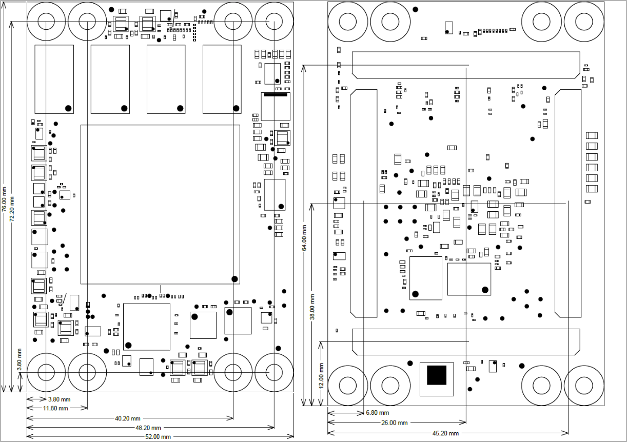 Image Removed Image Removed
|
Currently Offered Variants
| Scroll Title |
|---|
| anchor | Table_VCP_SO |
|---|
| title-alignment | center |
|---|
| title | Trenz Electronic Shop Overview |
|---|
|
| Scroll Table Layout |
|---|
| orientation | portrait |
|---|
| sortDirection | ASC |
|---|
| repeatTableHeaders | default |
|---|
style | widths | | sortByColumn | 1 |
|---|
| sortEnabled | false |
|---|
| cellHighlighting | true |
|---|
| Trenz shop TE0813 overview page |
|---|
| English page | German page |
| ASC | | repeatTableHeaders | default |
|---|
| style | |
|---|
| widths | |
|---|
| sortByColumn | 1 |
|---|
| sortEnabled | false |
|---|
| cellHighlighting | true |
|---|
|
| Parameter | Min | Max | Units | Reference Document |
|---|
| LP_DCDC 1) | 3.201 | 3.399 | V |
| | DCDCIN 1) | 3.135 | 3.465 | V |
| | GT_DCDC 1) | 3.201 | 3.399 | V |
| | PL_DCIN 1) 2) | 3.135 | 3.465 | V |
| | 3.3VIN | 3.135 | 3.465 | V |
| | PLL_3V3 | 3.135 | 3.465 | V |
| | PS_BATT | 1.2 | 1.5 | V | See FPGA datasheet. | | VCCO_47 | 1.164 | 3.399 | V | See FPGA datasheet. | | VCCO_48 | 1.164 | 3.399 | V | See FPGA datasheet. | | VCCO_64 | 0.97 | 1.854 | V | See FPGA datasheet. | VCCO_65 | 0.97 | 1.854 | V | See FPGA datasheet. | | VCCO_66 | 0.97 | 1.854 | V | See FPGA datasheet. | | VREF_64 | 0.6 | 1.2 | V | See FPGA datasheet. | | VREF_65 | 0.6 | 1.2 | V | See FPGA datasheet. | | VREF_66 | 0.6 | 1.2 | V | See FPGA datasheet. |
1) Dependent on the assembly option a higher input voltage may be possible. 2) This value depends highly on REV01 DCDC U4. Higher values may possible with different DCDCs or different revision. For more information consult schematic and according datasheets. |
Physical Dimensions
PCB thickness: 1.74 mm (± 10 %).
Revision History
Hardware Revision History
| Page properties |
|---|
|
Set correct links to download Carrier, e.g. TE0706 REV02:
TE0706-02 -> https://shop.trenz-electronic.de/Download/?path=Trenz_Electronic/Modules_and_Module_Carriers/4x5/4x5_Carriers/TE0706/REV02/Documents
Note:
Date format: YYYY-MM-DDExample:
| Date | Revision | Changes | Documentation Link |
|---|
| 2020-11-25 | REV02 | - Resistors R14 and R15 was replaced by 953R (was 5K1)
- Resistor R5 was replaced by 5K1, R8 by 953R (was 9K09 and 1K69 respectively)
| REV02 |
| Scroll Title |
|---|
| anchor | Figure_RV_HRN |
|---|
| title-alignment | center |
|---|
| title | Board hardware revision number. |
|---|
|
| Scroll Ignore |
|---|
| draw.io Diagram |
|---|
| border | true |
|---|
| diagramName | Figure_RV_HRN |
|---|
| simpleViewer | false |
|---|
width | | links | auto |
|---|
| tbstyle | top |
|---|
| lbox | true |
|---|
| diagramWidth | 188 |
|---|
| revision | 2 |
|---|
| Scroll Only |
|---|
 Image Removed Image Removed
|
| Scroll Title |
|---|
| anchor | Table_RH_HRH |
|---|
| title-alignment | center |
|---|
| title | Hardware Revision HistoryPhysical Dimension |
|---|
|
| scroll-ignore |
|---|
| draw.io Diagram |
|---|
| border | true |
|---|
| |
|---|
| diagramName | Figure_TS_PD |
|---|
| simpleViewer | true |
|---|
| width | |
|---|
| links | auto |
|---|
| tbstyle | top |
|---|
| diagramDisplayName | |
|---|
| lbox | true |
|---|
| diagramWidth | 611 |
|---|
| revision | 3 |
|---|
|
|
| Scroll Only |
|---|
| scroll-pdf | true |
|---|
| scroll-office | true |
|---|
| scroll-chm | true |
|---|
| scroll-docbook | true |
|---|
| scroll-eclipsehelp | true |
|---|
| scroll-epub | true |
|---|
| scroll-html | true |
|---|
| Image Added |
|
Currently Offered Variants
| Scroll Title |
|---|
| anchor | Table_VCP_SO |
|---|
| title-alignment | center |
|---|
| title | Trenz Electronic Shop Overview |
|---|
|
| Scroll Table Layout |
|---|
| orientation | portrait |
|---|
| sortDirection | ASC |
|---|
| repeatTableHeaders | default |
|---|
| style | |
|---|
| widths | |
|---|
| sortByColumn | 1 |
|---|
| sortEnabled | false |
|---|
| cellHighlighting | true |
|---|
|
|
Revision History
Hardware Revision History
| Scroll Title |
|---|
| anchor | Figure_RV_HRN |
|---|
| title-alignment | center |
|---|
| title | Board hardware revision number. |
|---|
|
| Scroll Ignore |
|---|
| draw.io Diagram |
|---|
| border | true |
|---|
| |
|---|
| diagramName | Figure_RV_HRN |
|---|
| simpleViewer | true |
|---|
| width | |
|---|
| links | auto |
|---|
| tbstyle | top |
|---|
| diagramDisplayName | |
|---|
| lbox | true |
|---|
| diagramWidth | 153 |
|---|
| revision | 3 |
|---|
|
|
| Scroll Only |
|---|
Image Added |
|
| Scroll Title |
|---|
| anchor | Table_RH_HRH |
|---|
| title-alignment | center |
|---|
| title | Hardware Revision History |
|---|
|
| Scroll Table Layout |
|---|
| orientation | portrait |
|---|
| sortDirection | ASC |
|---|
| repeatTableHeaders | default |
|---|
| style | |
|---|
| widths | |
|---|
| sortByColumn | 1 |
|---|
| sortEnabled | false |
|---|
| cellHighlighting | true |
|---|
|
tablelayout |
| orientation | portrait |
|---|
| sortDirection | ASC |
|---|
| repeatTableHeaders | default |
|---|
style | widths | | sortByColumn | 1 |
|---|
| sortEnabled | false |
|---|
| cellHighlighting | true |
|---|
| Date | Revision | Changes | Documentation Link |
|---|
| Date | Revision | Changes | Documentation Link |
|---|
| 2024-04 | REV02 | Changed DCDC (U13) from EN6347QI to MPM3860GQW-Z and apdated according circuit. Connected DDR4-TEN signals together for U2, U3, U9, and U12 and pulled them low via 499 Ohm resistor R127. Added testpoint TP3 for signal DDR4-TEN. Changed voltage rail from 1.35 V to 1.45 V via adaption voltage divider resistor R30 and changed voltage rail name PL_GT_1V35 to PL_GT_1V45. Changed voltage rail from 1.05 V to 1.15 V via adaption voltage divider resistors R33 and R35 and changed voltage rail name PL_GT_1V05 to PL_GT_1V15. Added diode D2 between U41 pin 3 net MR and voltage rail 3.3VIN. Added capacitors C202 ... C205 for VTT voltage rail VTT. Added resistors R124 (default: not fitted) and R125 to supply U4 VCC either from PL_DCIN or from 3.3VIN. Changed resistor R76 from 4.22 kOhm to 9.09 kOhm to set current limit to nearly 14.3 A for U4. Changed inductor (L9) from XGL4030-301MEC to XGL5030-351MEC. Added remote sense option (default: not fitted): R126 for U30. R128 for U29. R129 for U31.
Added decoupling capacitors: C208 for U4. C211, C212, and C213 for U6. C216 for U10. C214 for U26. C215 for U27. C210 for U34. C196 for U39. C197 for U40. C198 for U42. C199 for U41. C200 for U44. C201, C206, and C207 for U1.
Added pull-up resistors for HOLD (R130) and WP (R131) signals for Flash U7. Added pull-up resistors for HOLD (R132) and WP (R133) signals for Flash U17. Changed capacitor (C132) from 1 nF, X7R to 1.2 nF, NP0. Changed 10 nF capacitor (C112) from 16 V, 0402 to 10 V, 0201. Changed 100 nF capacitors (C37, C95, C96, C130, and C131) from 6.3 V, X5R, 0201 to 50 V, X7R, 0402. Changed capacitor (C76, C77, C134, C195) from 1 µF, 16 V to 2.2 µF, 10 V. Changed capacitor (C129, C140, C141, C142, C143, C144, C145, C146, C147, C148, C153) from 10 µF, 16 V to 22 µF, 10 V. Changed 22 uF capacitor (C70, C73, C74, C75) from 0805 to 0603. Changed 22 uF capacitor ( C78, C80, C81, C82, C83, C84, C85, C86, C87, C110, C152, C154, C178) from 6.3 V to 10 V. Changed 100 Ohm resistors (R7, R10) from 0201, 0.05 W to 0402, 0.063 W. Changed resistor R77 from 12 kOhm to 10 kOhm. Changed resistors R41 and R58 from 2 kOhm to 2.49 kOhm. Added testpoints TP4, TP10, TP11, TP13, TP14, TP19, TP21, TP22, TP33 ... TP72. Added UKCA logo. Updated from library. Changed signal trace length. Updated documentation.
| REV02 |
| - | REV01 | First Production Release | REV01 |
Hardware revision number can be found on the PCB board together with the module model number separated by the dash.
Document Change History
| Page properties |
|---|
|
- Note this list must be only updated, if the document is online on public doc!
- It's semi automatically, so do following
Add new row below first Copy "Page Information Macro (date)" Macro-Preview, Metadata Version number, Author Name and description to the empty row. Important Revision number must be the same as the Wiki document revision number Update Metadata = "Page Information Macro (current-version)" Preview+1 and add Author and change description. --> this point is will be deleted on newer pdf export template - Metadata is only used of compatibility of older exports
|
| Scroll Title |
|---|
| anchor | Table_RH_DCH |
|---|
| title-alignment | center |
|---|
| title | Document change history. |
|---|
|
| Scroll Table Layout |
|---|
| orientation | portrait |
|---|
| sortDirection | ASC |
|---|
| repeatTableHeaders | default |
|---|
| style | |
|---|
| widths | |
|---|
| sortByColumn | 1 |
|---|
| sortEnabled | false |
|---|
| cellHighlighting | true |
|---|
|
| Date | Revision | Contributor | Description |
|---|
| Page info |
|---|
| infoType | Modified date |
|---|
| dateFormat | yyyy-MM-dd |
|---|
| type | Flat |
|---|
|
| | Page info |
|---|
| infoType | Current version |
|---|
| prefix | v. |
|---|
| type | Flat |
|---|
| showVersions | false |
|---|
|
| | Page info |
|---|
| infoType | Modified by |
|---|
| type | Flat |
|---|
| showVersions | false |
|---|
|
| | | | | - Corrected max possible DDR4 assembly option
| | | | - Fixed issue in absolute maximum ratings
| | 2022-11-08 | v.13 | ED | | -- | all | | Page info |
|---|
| infoType | Modified users |
|---|
| type | Flat |
|---|
| showVersions | false |
|---|
|
| |
|
Disclaimer
| Include Page |
|---|
| IN:Legal Notices |
|---|
| IN:Legal Notices |
|---|
|