Page History
...
| Scroll pdf title | ||
|---|---|---|
| ||
|

SPI signals on the TE0300 are listed and described in the table below.
...
| Warning |
|---|
| Any other usage of the SPI bus is neither supported nor recommended. |
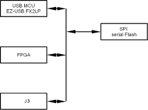
SPI bus for configuration
The SPI bus is used for configuration in two ways by default:
...
The PROM file (containing the FPGA configuration bitstream) can be written to the SPI serial Flash memory (slave) also through the SPI pins of J3 (attached device set to master mode). In this case, the FPGA shall be turned off or three-stated to release its shared SPI pins and the USB FX2 microcontroller shall three-state (Z = high impedance) its shared SPI pins.
SPI bus for operation
A plurality of usage combinations of the SPI bus during operation is made available to the user as suggested in Table B below.
| Scroll pdf title | ||||||||||||||||||||||||||||||||||||
|---|---|---|---|---|---|---|---|---|---|---|---|---|---|---|---|---|---|---|---|---|---|---|---|---|---|---|---|---|---|---|---|---|---|---|---|---|
| ||||||||||||||||||||||||||||||||||||
|
| Warning |
|---|
| Other combinations of master and slave units are neither supported nor recommended. |
SPI Header Connector J3
The offset holes of header J3 allow a removable press fit of standard 0.100 inch header pins to connect flying leads without any soldering necessary.
SPI signals are made available on the dedicated header J3 accessible through an SPI programmer with flying leads as described in the table below.
| Scroll pdf title | ||||||||||
|---|---|---|---|---|---|---|---|---|---|---|
| ||||||||||
|


Overview
Content Tools