Page History
...
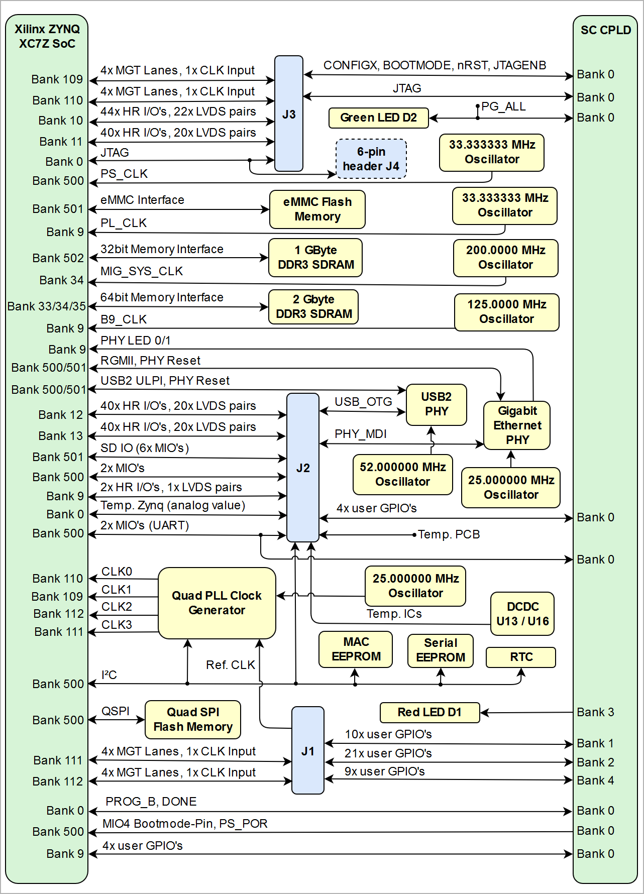
- Xilinx Zynq-7000 XC7Z045-2FFG900I SoC
- Rugged for shock and high vibration
- Large number of configurable I/Os are provided via rugged high-speed stacking strips
- Dual ARM Cortex-A9 MPCore
- 1 GByte RAM (32bit wide DDR3) connected to PS
- 2 GByte RAM (64bit wide DDR3) connected to PL
- 32 MByte QSPI Flash memory
- Hi-Speed USB2 ULPI transceiver PHY
- Gigabit (10/100/1000 Mbps) Ethernet transceiver PHY
- 4 GByte eMMC (optional up to 64 GByte)
- Lattice MachXO2 HC 4000 System Controller CPLD
- 40 GPIO's available to user on B2B connector
- MAC-address EEPROM
- Serial user EEPROM
- Temperature compensated RTC (real-time clock)
- Si5338A programmable quad PLL clock generator for GTX transceiver clocks
- Plug-on module with 3 x 160-pin high-speed strips
- 16 GTX high-performance transceiver
- 4x GT transceiver clock inputs
- 254 166 FPGA I/O's (125 83 LVDS pairs)
- On-board high-efficiency switch-mode DC-DC converters
- System management
- eFUSE bit-stream encryption
- AES bit-stream encryption
- Evenly-spread supply pins for good signal integrity
- User LED
...
| Scroll Title | ||||||||||||||||||||||||||||||||
|---|---|---|---|---|---|---|---|---|---|---|---|---|---|---|---|---|---|---|---|---|---|---|---|---|---|---|---|---|---|---|---|---|
| ||||||||||||||||||||||||||||||||
|
...
| Storage device name | Content | Notes |
|---|---|---|
| 24LC128-I/ST EEPROM | not not programmed | User content |
24AA025E48 EEPROM | User content not programmed | Valid MAC Address from manufacturer |
| Si5338A OTP Area | not programmed | - |
| eMMC Flash Memory | Empty, not programmed | Except serial number programmed by flash vendor |
SPI Flash OTP Area | Empty, not programmed | Except serial number programmed by flash vendor |
SPI Flash Quad Enable bit | Programmed | - |
SPI Flash main array | demo design | - |
eFUSE USER | Not programmed | - |
eFUSE Security | Not programmed | - |
...
The TE0783 boot mode is selected by the pin 'CPLD_GPIO3' of the SC CPLD, which is connected to B2B pin J2-16 to either boot from the on-board QSPI Flash memory U38 or SD IO interface. See section Bootmode in the TE0783 SC CPLD reference Wiki page.
...
Special purpose pins are connected to System Controller CPLD (U32) and have following default configuration:
| Pin Name | Direction | Function | Default Configuration |
|---|---|---|---|
| EXT_IO1 ... EXT_IO40 | in / out | user GPIO on B2B | see current CPLD firmware |
| BOOTMODE | in | in | signal forwarded to MIO9 and currently used as UART RX line |
| CONFIGX | in | out | signal forwarded to MIO8 and currently used as UART TX line |
| NRST_IN | in | nRESET input | external Board Reset |
| M_TDO | out | CPLD JTAG interface | - |
| M_TDI | in | ||
| M_TCK | in | ||
| M_TMS | in | ||
| JTAGENB | in | enable JTAG | pull high for programming SC CPLD firmware |
| ETH1_RESET | out | reset GbE PHY U18 | see current SC CPLD firmware |
| OTG-RST | out | reset USB2 PHYs U4 and U8 | see current SC CPLD firmware |
| DONE | in | Zynq control signal | PL configuration completed |
| PROG_B | out | PL configuration reset signal | |
| PS_POR | out | PS power-on reset | |
| BM2/MIO4 | out | Bootmode Pin: SD or QSPI | |
| MIO14 | in | user MIO pins | currently used as UART interface |
| MIO15 | out | ||
| LED2 | out | Red LED D1 status signal | see current CPLD firmware |
| CPLD_GPIO0 ... CPLD_GPIO3 | in / outuser GPIO on B2B | CPLD_GPIO3 used for Boot Mode | see current CPLD firmware |
| FPGA_CPLD1 ... FPGA_CPLD4 | in /out | user GPIO to FPGA bank 9 | see current SC CPLD firmware |
| EN_1V | out | Power control | enable signal DCDC U13 '1V' |
| PG_ALL | in | power good signal all voltages powered up properly → Green LED D2 lights up. |
...
GbE PHY connection:
| PHY PIN | Zynq PS / PL | System Controller CPLD | Notes |
|---|---|---|---|
| MDC/MDIO | MIO52, MIO53 | -- | |
| LED0 | Bank 9, Pin AC18 | -- | |
| LED1 | Bank 9, Pin AC19 | -- | |
| Interrupt- | - | not connected | |
| CLK125 | - | - | 125 MHz clock output not connected |
| CONFIG | - | - | When pin connected to GND, PHY Address is strapped to 0x00 by default |
| RESETn | MIO7 | -ETH1_RESET33 (MIO7) → voltage level translator U30 → ETH1_RESET | |
| RGMII | MIO16..MIO27 | - | |
| MDI | - | - | on B2B J2 connector |
Table 9: General overview of the Gigabit Ethernet1 PHY signals
...
USB2 PHY connection:
| PHY Pin | Zynq PS / PL | CPLD | B2B Connector J2 | Notes |
|---|---|---|---|---|
| ULPI | MIO28..39 | - | - | Zynq USB0 MIO pins are connected to the PHY |
| REFCLK | - | - | - | 52MHz from on board oscillator (U7) |
| REFSEL[0..2]- | - | - | 000 GND, select 52MHz reference Clock | |
| RESETB | MIO0 | OTG_RESET33- | OTG-RESET33 → voltage level translator U30 → OTG-RESET | |
| CLKOUT | MIO36 | -- | Connected to 1.8V selects reference clock operation mode | |
| DP,DM- | - | USB1_D_P, USB1_D_N | USB Data lines | |
| CPEN | - | - | VBUS1_V_EN | External USB power switch active high enable signal |
| VBUS- | - | USB1_VBUS | Connect to USB VBUS via a series resistor. Check reference schematic. | |
| ID- | - | OTG1_ID | For an A-Device connect to ground, for a B-Device left floating |
Table 10: General overview of the Gigabit Ethernet2 PHY signals
...
eMMC Flash memory device (U28) is connected to the Zynq PS MIO bank 501 pins MIO46..MIO51. eMMC chips MTFC4GMVEA-4M IT (Flash NAND-IC 2x 16 Gbit) is used with 4 GByte of memory density.
...
DDR3L Memory
By default TE0783-01 module has two 16-bit 16bit wide IM (Intelligent Memory) IM4G16D3FABG-125I DDR3L SDRAM (DDR3-1600 Speedgrade) connected to the PS DDR memory bank 502, the chips are arranged into 32-bit 32bit wide memory bus providing total of 1 GBytes of on-board RAM.
Another 4 chips are arranged into 64bit wide memory bus prodivding total of 2 GByte on-board RAM connected to the PL HP banks 34, 35 and 36.
Quad SPI Flash MemoryQuad SPI Flash Memory
One quad SPI compatible serial bus Flash memory (U38) for FPGA configuration file storage is provided by Spansion S25FL256SAGBHI20 with 256 Mbit (32 MByte) memory density. After configuration completes the remaining free memory can be used for application data storage. All four SPI data lines are connected to the FPGA allowing x1, x2 or x4 data bus widths to be used. The maximum data transfer rate depends on the bus width and clock frequency.
...
| Signal | Frequency | Notes |
|---|---|---|
| IN1/IN2 | user | External clock signal supply from B2B connector J3, pins J3-38 / J3-40 |
IN3 | 25.000000 MHz | Fixed input clock signal from reference clock generator SiT8008BI-73-18S-25.000000E (U3) |
| IN4 | - | LSB of the default I2C address, wired to ground mean address is 0x70 |
IN5 | - | Not connected |
IN6 | - | Wired to ground |
| CLK0 A/B | - | reference clock 0 of Bank 112 GTX |
CLK1 A/B | - | reference clock 1 of Bank 111 GTX |
CLK2 A/B | - | reference clock 0 of Bank 110 GTX |
| CLK3 A/B | - | reference clock 1 of Bank 109 GTX |
Table 1412: General overview of the on-board quad clock generator I/O signals
...
| Clock Source | Schematic Name | Frequency | Clock Destination | |||
|---|---|---|---|---|---|---|
| SiTime SiT8008AI oscillator, U61 | PS_CLK | 33.333333 MHz | Zynq SoC U1, pin A22 | |||
| SiTime SiT8008BI SiT8008AI oscillator, U21U33 | -PL_CLK | 2533.000000 333333 MHz | Quad PLL clock generator U2Zynq SoC U1, pin 3AA18 | |||
| SiTime SiT8008AI Microchip DSC1123 oscillator, U7U15 | MIG_SYS_CLK_P / MIG_SYS_CLK_N | 200.0000 MHz | Zynq SoC U1, pins H9, G9 | |||
| SiTime SiT8008BI oscillator, U3 | - | 25.000000 MHz | Quad PLL clock generator U2, pin 3 | |||
| Microchip DSC1123 oscillator, U31 | B9_CLK_P, B9_CLK_N | 125.0000 MHz | Zynq SoC U1, pins AD18, AD19 | |||
| SiTime SiT8008AI oscillator, U7 | - | 52.000000 MHz | USB2 PHYs U4 and U8, pin | - | 52.000000 MHz | USB2 PHYs U4 and U8, pin 26 |
| SiTime SiT8008BI oscillator, U11 | - | 25.000000 MHz | GbE PHYs U18 and U20, pin 34 |
Table 1513: Reference clock signals
On-board LEDs
| LED | Color | Connected to | Description and Notes | |
|---|---|---|---|---|
| D1 | Red | System Controller CPLD U14U32, bank 3 | Exact function is defined by SC CPLD firmware0 | Indicates power-up sequence completed. |
| D2 | Green | System Controller CPLD U14U32, bank 32 | Exact function is defined by SC CPLD firmware. |
Table 1614: On-board LEDs
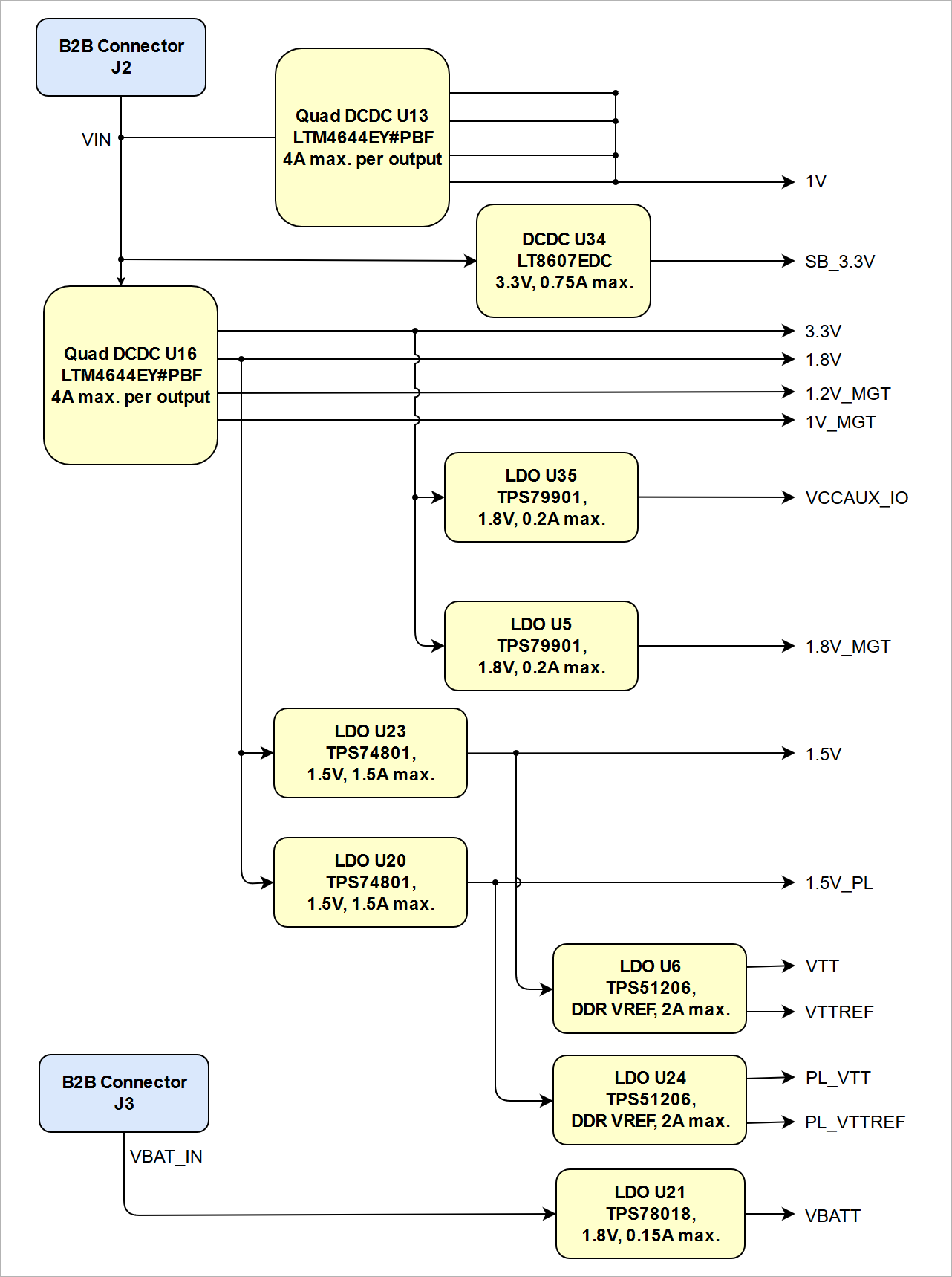
Power and Power-on Sequence
...
Power supply with minimum current capability of 3A 4A for system startup is recommended.
...
| Power Input | Typical Current |
|---|---|
| VIN | TBD* |
| C3.3V | TBD* |
Table 1715: Power consumption
* TBD - To Be Determined soon with reference design setup.
Single 3.3V power supply with minimum current capability of 4A for system startup is recommended.
For the lowest power consumption and highest efficiency of the on-board DC-DC regulators it is recommended to power the module from one single 3.3V supply. All input power supplies should have a nominal value of 3.3V. Although the input power supplies can be powered up in any order, it is recommended to power them up simultaneously.
| Warning |
|---|
| To avoid any damage to the module, check for stabilized on-board voltages should be carried out (i.e. power good and |
| Warning |
| To avoid any damage to the module, check for stabilized on-board voltages should be carried out (i.e. power good and enable signals) before powering up any Zynq's I/O bank voltages VCCO_x. All I/Os should be tri-stated during power-on sequence. |
Power Distribution Dependencies
...
| anchor | Figure_3 |
|---|---|
| title | Figure 3: TE0783-01 Power Distribution Diagram |
...
The Trenz TE0783 SoM is equipped with two quad DC-DC voltage regulators to generate required on-board voltage levels 1V, 3.3V, 1.8V, 1.2V_MGT, 1V_MGT. Additional voltage regulators are used to generate voltages 3.3V_SB, 1.5V, VTT, VTTREF for PS and PL memory bank, 1.8V_MGT and VCCAUX_IO.
There are following dependencies how the initial voltages of the power rails on the B2B connectors are distributed to
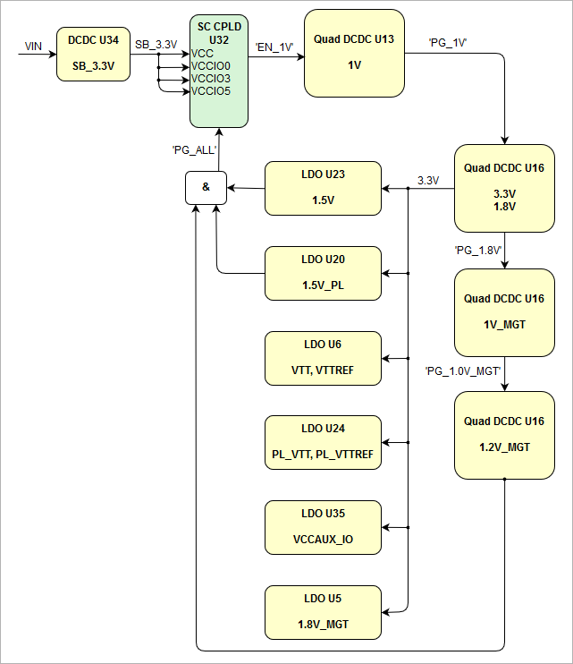
Power-On Sequence
The TE0820 SoM meets the recommended criteria to power up the Xilinx Zynq chip properly by keeping a specific sequence of enabling the on-board DC-DC converters dedicated to the particular functional units of the Zynq chip and powering up the on-board voltages.Following diagram clarifies the sequence of enabling the , which power up further DC-DC converters and the particular on-board voltages, which will power-up in descending order as listed in the blocks of the diagram:
| Scroll Title | |||||||||||||||||||||||||||||||
|---|---|---|---|---|---|---|---|---|---|---|---|---|---|---|---|---|---|---|---|---|---|---|---|---|---|---|---|---|---|---|---|
| |||||||||||||||||||||||||||||||
|
...
It is important that all carrier board I/Os are 3-stated at power-on until System Controller CPLD sets PGOOD signal high (B2B connector JM1, pin 30), or 3.3V is present on B2B connector JM2 pins 10 and 12, indicating that all on-module voltages have become stable and module is properly powered up.
...
|
See also Xilinx datasheet DS191 for additional information. User should also check related base board documentation when intending base board design for TE0783 module.
Power-On Sequence
Power-on sequence is handled by the System Controller CPLD using "Power good"-signals from the voltage regulators:
| Scroll Title | ||||||||||||||||||||||||||||||||
|---|---|---|---|---|---|---|---|---|---|---|---|---|---|---|---|---|---|---|---|---|---|---|---|---|---|---|---|---|---|---|---|---|
| ||||||||||||||||||||||||||||||||
|
Voltage Monitor Circuit
The voltages '1V' and '3.3V' are monitored by the voltage monitor circuit U27, which generates the PS_POR reset signal if monitored voltages have transient interruptions:
| Scroll Title | ||||||||||||||||||||||||||||||||
|---|---|---|---|---|---|---|---|---|---|---|---|---|---|---|---|---|---|---|---|---|---|---|---|---|---|---|---|---|---|---|---|---|
| ||||||||||||||||||||||||||||||||
|

Power Rails
| Power Rail Name on B2B Connector | J1 Pins | J2 Pins | J3 Pins | Direction | Notes | |||||
|---|---|---|---|---|---|---|---|---|---|---|
| VIN | - | 165, 166, 167, 168 | - | Input | external power supply voltage | |||||
| C3.3V | - | 147, 148 | - | Inputexternal 3.3V power supply voltage | Normally leave unconnected | |||||
| 3.3V | - | 111, 112, 123, 124, 135 136 169, 170, 171, 172 | - | Output | internal 3.3V voltage level | |||||
| 1.8V | 169, 170, 171, 172 | - | - | Output | internal 1.8V voltage level | |||||
| EXT_IO_VCC | 99, 100 | - | - | Input | SC CPLD bank 1, 2 and 4 voltage | |||||
| VCCIO_10 | - | - | 99, 100 | Input | high range I/O bank voltage | |||||
| VCCIO_11 | - | - | 159, 160 | Input | high range I/O bank voltage | |||||
| VCCIO_12 | - | 159, 160 | - | Input | high range I/O bank voltage | |||||
| VCCIO_13 | - | 99, 100 | - | Input | high range I/O bank voltageVCCIO_33 | 99, 100 | - | - | Input | high performance I/O bank voltage |
| VCCIO_34 | 159, 160 | - | - | Input | high performance I/O bank voltage | |||||
| VBAT_IN | - | - | 124 | Input | backup battery voltage |
Table 1816: Module power rails
Bank Voltages
| Bank | Schematic Name | Voltage | Range | Notes | ||
|---|---|---|---|---|---|---|
| 0 | - | 3.3 V | - | FPGA configuration | ||
| 502 | - | 1.5 V | - | DDR3-RAM port | ||
| 109 / 110 / 111 / 112 | - | 1.2 V | - | MGT | ||
| 500 / | - | 3.3 V | - | PS MIO banks | ||
| 501 | - | 31. | 3 V8V | - | PS MIO banks | |
| 9 (HR) | - | 13.8 3 V | 1.2V to 3.3V | - | -ETH2 RGMII | |
| 10 (HR) | VCCIO_10 | user | 1.2V to 3.3V | - | ||
| 11 (HR) | VCCIO_11 | user | 1.2V to 3.3V | - | ||
| 12 (HR) | VCCIO_12 | user | 1.2V to 3.3V | - | ||
| 13 (HR) | VCCIO_13 | user | 1.2V to 3.3V | - | ||
| 33 (HP) | VCCIO_33 | user1.5V_PL | 1.2V to 1.8V-5 V | - | 64bit DDR3L SD-RAM | |
| 34 (HP) | VCCIO_34 | user1.5V_PL | 1.2V to 1.8V5 V | - | ||
| 35 (HP) | - | 1.8 V5V_PL | 1.2V to 1.8V | Hyper-RAM, Ethernet, I²C | 5 V | - |
Table 17Table 19: Module I/O bank voltages
See Xilinx Zynq-7000 datasheet DS191 for the voltage ranges allowed.
Board to Board Connectors
.
Board to Board Connectors
| Include Page | ||||
|---|---|---|---|---|
|
Variants Currently In Production
...
Parameter | Min | Max | Units | Notes | |||||
|---|---|---|---|---|---|---|---|---|---|
VIN supply voltage | -0.3 | 15 | V | LTM4644 datasheet | |||||
| C3.3V VBAT supply voltage | -0.3 | 3.6 | V | LTM4644 TPS780180 datasheet | |||||
| PS I/O supply voltage, VCCO_PSIO | -0.5 | 3.6 | V | Xilinx document DS191 | |||||
| PS I/O input voltage | -0.4 | VCCO_PSIO + 0.55 | V | Xilinx document DS191 | |||||
| HP I/O bank supply voltage, VCCO | -0.5 | 2.0 | V | Xilinx document DS191 | |||||
| HP I/O bank input voltage | -0.55 | VCCO + 0.55 | V | Xilinx document DS191 | |||||
| HR I/O bank supply voltage, VCCO | -0.5 | 3.6 | V | Xilinx document DS191 | |||||
| HR I/O bank input voltage | -0.55 | VCCO + 0.55 | V | Xilinx document DS191 | Reference Voltage pin | -0.5 | 2 | V | Xilinx document DS191 |
| Differential input voltage | -0.4 | 2.625 | V | Xilinx document DS191 | |||||
| MGT reference clocks absolute input voltage | -0.5 | 1.32 | V | Xilinx document DS191 | |||||
| MGT absolute input voltage | -0.5 | 1.26 | V | Xilinx document DS191 | |||||
Voltage on SC CPLD pins | -0.5 | 3.75 | V | Lattice Semiconductor MachXO2 datasheet | |||||
Storage temperature | -40 | +85 | °C | See eMMC MTFC4GMVEA eMMC MTFC4GACAJCN datasheet |
Table 2018: Module absolute maximum ratings
...
| Parameter | Min | Max | Units | Notes | |
|---|---|---|---|---|---|
| VIN supply voltage | 11.4 | 1412.6 | V | See LTM4644 datasheet | 12V nominal power supply voltage |
| VBAT C3.3V supply voltage | 32.323 | 5.4655 | V | See LCMXO2-256HC, LTM4644 TPS780180 datasheet | |
| PS I/O supply voltage, VCCO_PSIO | 1.710 | 3.465 | V | Xilinx document DS191 | |
| PS I/O input voltage | –0.20 | VCCO_PSIO + 0.20 | V | Xilinx document DS191 | |
| HP I/O banks supply voltage, VCCO | 1.14 | 1.89 | V | Xilinx document DS191 | |
| HP I/O banks input voltage | -0.20 | VCCO + 0.20 | V | Xilinx document DS191 | |
| HR I/O banks supply voltage, VCCO | 1.14 | 3.465 | V | Xilinx document DS191 | |
| HR I/O banks input voltage | -0.20 | VCCO + 0.20 | V | Xilinx document DS191 | |
| Differential input voltage | -0.2 | 2.625 | V | Xilinx document DS191 | |
| Voltage on SC CPLD pins | -0.3 | 3.6 | V | Lattice Semiconductor MachXO2 datasheet | |
| Operating Temperature Range | -40 | 85 | °C | Xilinx document DS191, industrial grade Zynq temperarure range |
Table 2119: Recommended operating conditions
...
| Scroll Title | ||||
|---|---|---|---|---|
| ||||
|
...
| Date | Revision | Notes | PCN Link | Documentation Link |
|---|---|---|---|---|
| - | 01 | first production release | - | TE0783-01 |
Table 2220: Hardware revision history table
...
| Scroll Title | ||||
|---|---|---|---|---|
| ||||
|
...
Date | Revision | Contributors | Description | ||||||||||||||||||||||||||
|---|---|---|---|---|---|---|---|---|---|---|---|---|---|---|---|---|---|---|---|---|---|---|---|---|---|---|---|---|---|
|
|
|
| ||||||||||||||||||||||||||
| 2018-08-07 | v.18 | Ali Naseri |
| ||||||||||||||||||||||||||
| -- | all |
|
|
Table 21Table 23: Document change history
Disclaimer
| Include Page | ||||
|---|---|---|---|---|
|
Overview
Content Tools