Page History
...
- XPS, if MicroBlaze is not used
EDK (or both), if MicroBlaze is used.
The Logic Architecture Layer could be loaded from SPI Flash or from JTAG and/or USB connections. See here.
| Note |
|---|
A TE USB FX2 module comes with SPI Flash preloaded with a reference design. Those preloaded image is just for getting started demo. For real designs:
|
...
Preloaded Logic Architecture Layer (in SPI Flash): Reference Architecture Layer description
...
The reference design architecture was built using Xilinx Embedded Development Kit (EDK). Basically, it is an embedded system on a chip with a Xilinx MicroBlaze 32-bit soft microprocessor. The MicroBlaze (MB) initializes and sets up the system.
...
| Scroll pdf title | ||
|---|---|---|
| ||
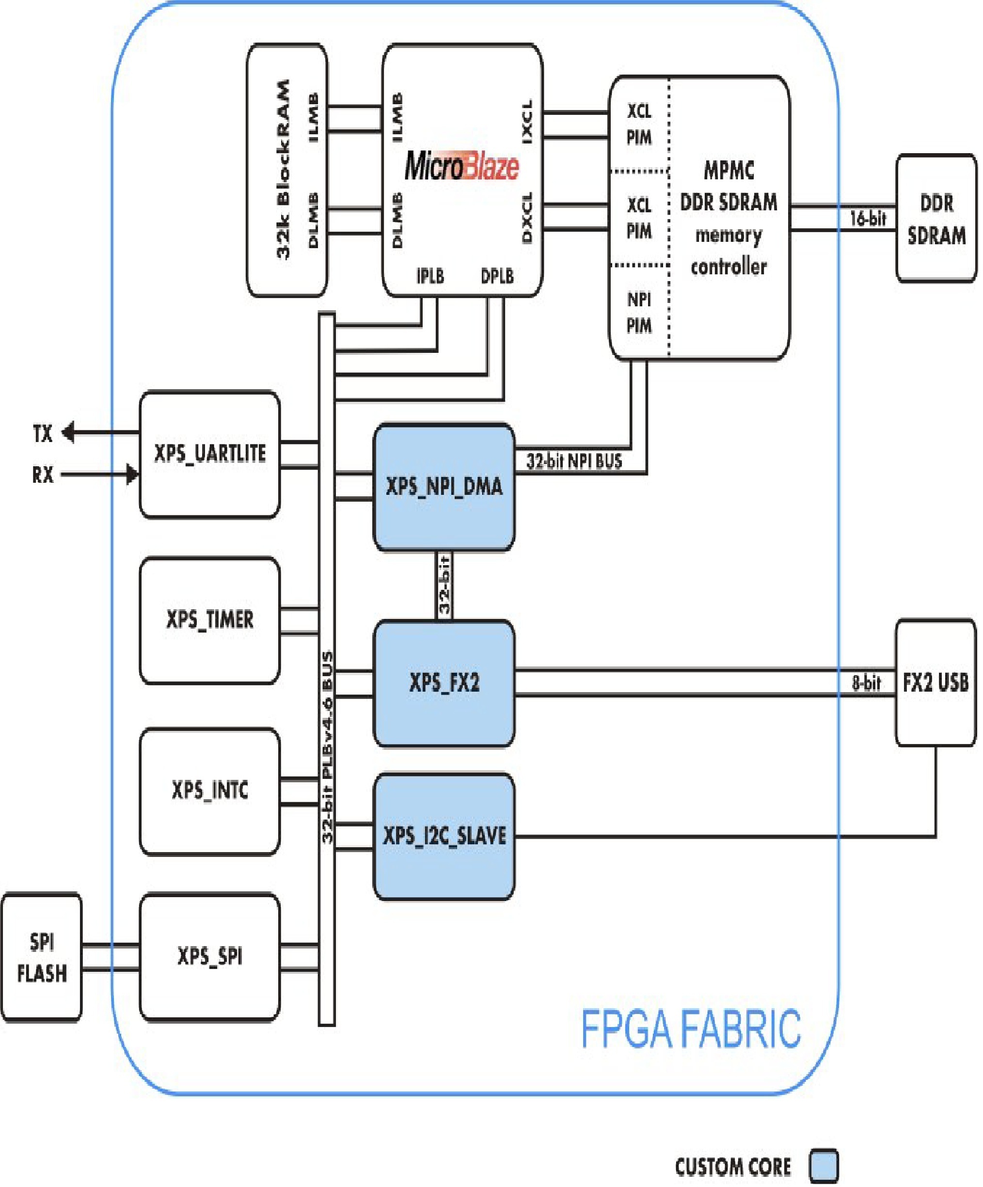 |
XPS_I2C_SLAVE custom IP block
It is a logic block for low speed bidirectional communication between the FPGA and a host PC. It is usually used for command, settings and status communication. It contains 6 × 32-bit memory mapped registers:
...
MicroBlaze Driver code: here.
XPS_NPI_DMA custom IP block
It is a high speed DMA (direct memory access) engine which connects to the MPMC (Multi-Port Memory Controller) VFBC (Video Frame Buffer Controller) port. It enables high speed data streaming to/from external memory (DDR SDRAM) and multiple sources. It can be controlled by a processor using 6 × 32-bit memory mapped registers attached to the PLB (peripheral local bus). For more information about registers, see Xilinx LogiCORE IP Multi-Port Memory Controller (MPMC) data sheets (Xilinx DS643), Video Frame Buffer Controller PIM section.
When data is sent from the USB-host to a USB FX2 module high-speed endpoint (high speed communication channel), it is automatically stored into the RAM by the custom built DMA engine (XPS_NPI_DMA) at a specified buffer location. The reference design software running on the MicroBlaze verifies the transferred data at the end of transmission and sends to the USB host a notification about the data test (passed / failed).
...
MicroBlaze Driver code: here.
XPS_FX2 custom IP block
It is a logic block for high speed bidirectional communication between the FPGA and a host PC. It contains 2 kbyte FIFOs for data buffering. More information about the 5 × 32-bit memory mapped registers is contained in the #project_root#/pcores/xps_fx2_v1_00_a/doc/ folder of the reference design project folder.
When data is sent form a USB FX2 module high-speed endpoint to the USB host, it is automatically fetched from the RAM via the custom DMA engine (XPS_NPI_DMA) and forwarded to the XPS_FX2 core in 1-kbyte packets. MicroBlaze throttles the throughput to prevent XPS_FX2 TX FIFO overflow.
...
MicroBlaze Driver code: here.
Source Code of the reference architecture
The source code of the reference architecture of the Trenz Electronic USB FX2 Technology Stack is released on GitHub (TE0300, TE0320 and TE0630).
Overview
Content Tools