Page History
...
| Scroll Title | ||||||||||||||||||||||||||||||||||||||
|---|---|---|---|---|---|---|---|---|---|---|---|---|---|---|---|---|---|---|---|---|---|---|---|---|---|---|---|---|---|---|---|---|---|---|---|---|---|---|
| ||||||||||||||||||||||||||||||||||||||
|
...
| Scroll Title | |||||||||||||||||||||||||||||||||||||||||||||||||||||||||||||||
|---|---|---|---|---|---|---|---|---|---|---|---|---|---|---|---|---|---|---|---|---|---|---|---|---|---|---|---|---|---|---|---|---|---|---|---|---|---|---|---|---|---|---|---|---|---|---|---|---|---|---|---|---|---|---|---|---|---|---|---|---|---|---|---|
| |||||||||||||||||||||||||||||||||||||||||||||||||||||||||||||||
|
...
Software Setup
Download RF Analyzer GUI from the following link and install it.
Hardware Setup
The Hardware contains of a TE0835 module and TEB0835 carrier board and has 8 ADC inputs and 8 DAC outputs.
- Plug the TE0835 module on the TEB0835 carrier board
- Install the cooler on the RFSoC
- Connect the micro USB cable to the J29 connector
- Plug the 12V power supply cable to the J19 connector
- Plug the prepared SD card on the SD card socket (J28)
- Connect a cable with SMA or SMT connector to one of the DAC connector( for example DAC0 J9) and feed it back to the related ADC input (for example ADC0 J1)
- (optional) A signal generator can be used to feed desired sinal to ADC input.
- (optional) An oscilloscope can be used to monitor the output signal of DAC.
...
DAC6_OUT
...
Design Flow
| Page properties | ||||
|---|---|---|---|---|
| ||||
Notes :
|
| Note |
|---|
Reference Design is available with and without prebuilt files. It's recommended to use TE prebuilt files for first lunch. |
Trenz Electronic provides a tcl based built environment based on Xilinx Design Flow.
See also:
- Xilinx Development Tools#XilinxSoftware-BasicUserGuides
- Vivado Projects - TE Reference Design
- Project Delivery.
The Trenz Electronic FPGA Reference Designs are TCL-script based project. Command files for execution will be generated with "_create_win_setup.cmd" on Windows OS and "_create_linux_setup.sh" on Linux OS.
TE Scripts are only needed to generate the vivado project, all other additional steps are optional and can also executed by Xilinx Vivado/SDK GUI. For currently Scripts limitations on Win and Linux OS see: Project Delivery Currently limitations of functionality
- _create_win_setup.cmd/_create_linux_setup.sh and follow instructions on shell:
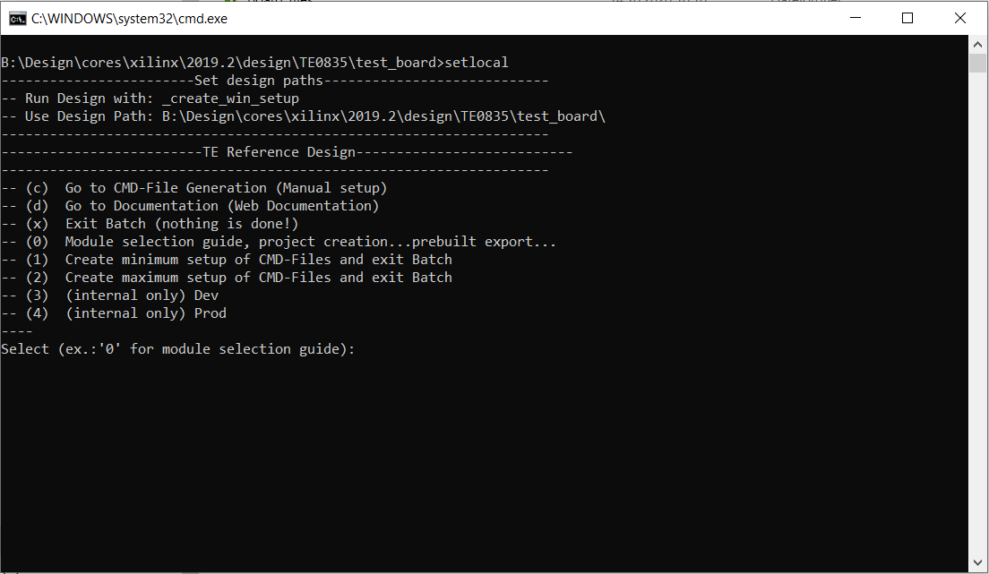
- Press 0 and enter to start "Module Selection Guide"
- (optional Win OS) Generate Virtual Drive or use short directory for the reference design (for example x:\<design name>)
- Create Project (follow instruction of the product selection guide), settings file will be configured automatically during this process)
- (optional for manual changes) Select correct device and Xilinx install path on "design_basic_settings.cmd" and create Vivado project with "vivado_create_project_guimode.cmd"
Note: Select correct one, see alsoTE Board Part Files
- (optional for manual changes) Select correct device and Xilinx install path on "design_basic_settings.cmd" and create Vivado project with "vivado_create_project_guimode.cmd"
- Create XSA and export to prebuilt folder
- Run on Vivado TCL: TE::hw_build_design -export_prebuilt
Note: Script generate design and export files into \prebuilt\hardware\<short dir>. Use GUI is the same, except file export to prebuilt folder
- Run on Vivado TCL: TE::hw_build_design -export_prebuilt
- Create Linux (bl31.elf, uboot.elf and image.ub) with exported XSA
- XSA is exported to "prebuilt\hardware\<short name>"
Note: HW Export from Vivado GUI create another path as default workspace. - Create Linux images on VM, see PetaLinux KICKstart
- Use TE Template from /os/petalinux
- XSA is exported to "prebuilt\hardware\<short name>"
- Add Linux files (bl31.elf, uboot.elf and image.ub) to prebuilt folder
- "prebuilt\os\petalinux\<ddr size>" or "prebuilt\os\petalinux\<short name>"
- Generate Programming Files with Vitis
- Run on Vivado TCL: TE::sw_run_vitis -all
Note: Scripts generate applications and bootable files, which are defined in "sw_lib\apps_list.csv" - (alternative) Start SDK with Vivado GUI or start with TE Scripts on Vivado TCL: TE::sw_run_vitis
Note: TCL scripts generate also platform project, this must be done manuelly in case GUI is used. See Vitis
- Run on Vivado TCL: TE::sw_run_vitis -all
Launch
...
| Page properties | ||||
|---|---|---|---|---|
| ||||
| Notes Note: Basic Design Steps
|
Programming
| Note |
|---|
Reference Design is available with and without prebuilt files. It's recommended to use TE prebuilt files for first lunch. |
Trenz Electronic provides a tcl based built environment based on Xilinx Design Flow.
See also:
- Xilinx Development Tools#XilinxSoftware-BasicUserGuides
- Vivado Projects - TE Reference Design
- Project Delivery.
...
Check Module and Carrier TRMs for proper HW configuration before you try any design. |
Xilinx documentation for programming and debugging: Vivado/SDK/SDSoC-Xilinx Software Programming and Debugging
Get prebuilt boot binaries
- _create_win_setup.cmd
...
- /_create_linux_setup.sh
...
- and follow instructions on shell
- Press 0 and enter to start "Module Selection Guide"
- Select assembly version
- Validate selection
- Select Create and open delivery binary folder
Note: Folder (<project foler>/_binaries_<Artikel Name>) with subfolder (boot_<app name>) for different applications will be generated
QSPI
Optional for Boot.bin on QSPI Flash and image.ub on SD.
- Connect JTAG and power on carrier with module
- Open Vivado Project with "vivado_open_existing_project_guimode.cmd" or if not created, create with "vivado_create_project_guimode.cmd"
- Type on Vivado TCL Console: TE::pr_program_flash -swapp u-boot
Note: To program with SDK/Vivado GUI, use special FSBL (zynqmp_fsbl_flash) on setup
optional "TE::pr_program_flash -swapp hello_te0835" possible - Copy image.ub on SD-Card
- use files from (<project foler>/_binaries_<Articel Name>)/boot_linux from generated binary folder,see: Get prebuilt boot binaries
- or use prebuilt file location, see <design_name>/prebuilt/readme_file_location.txt
- Insert SD-Card
SD
- Copy image.ub and Boot.bin on SD-Card
- use files from (<project foler>/_binaries_<Articel Name>)/boot_linux from generated binary folder,see: Get prebuilt boot binaries
- or use prebuilt file location, see <design_name>/prebuilt/readme_file_location.txt
- Set Boot Mode to SD-Boot.
- Depends on Carrier, see carrier TRM.
- Insert SD-Card in SD-Slot.
JTAG
Not used on this Example.
Usage
- Prepare HW like described on section TE0835 Test Board#Hardware Setup
- Connect UART USB (most cases same as JTAG)
- Select SD Card as Boot Mode (or QSPI - depending on step 1)
Note: See TRM of the Carrier, which is used. - Power On PCB
Note: 1. Zynqmp RFSoC Boot ROM loads FSBL from SD into OCM, 2. FSBL loads U-boot from SD into DDR, 3. U-boot load Linux from SD into DDR
Linux
- Open Serial Console (e.g. putty)
- Speed: 115200
- COM Port: Win OS, see device manager, Linux OS see dmesg |grep tty (UART is *USB1)
- Linux Console:
Note: Wait until Linux boot finished For Linux Login use:- User Name: root
- Password: root
- You can use Linux shell now.
- I2C 0 Bus type: i2cdetect -y -r 0
- I2C 1 Bus type: i2cdetect -y -r 1
- RTC check: dmesg | grep rtc
- ETH0 works with udhcpc
- USB type "lsusb" or connect USB2.0 device
- Option Features
- Webserver to get access to Zynqmp RFSoC
- insert IP on web browser to start web interface
- init.sh scripts
- add init.sh script on SD, content will be load automatically on startup (template included in ./misc/SD)
- add init.sh script on SD, content will be load automatically on startup (template included in ./misc/SD)
- Webserver to get access to Zynqmp RFSoC
Vivado HW Manager
| Page properties | ||||
|---|---|---|---|---|
| ||||
Note:
|
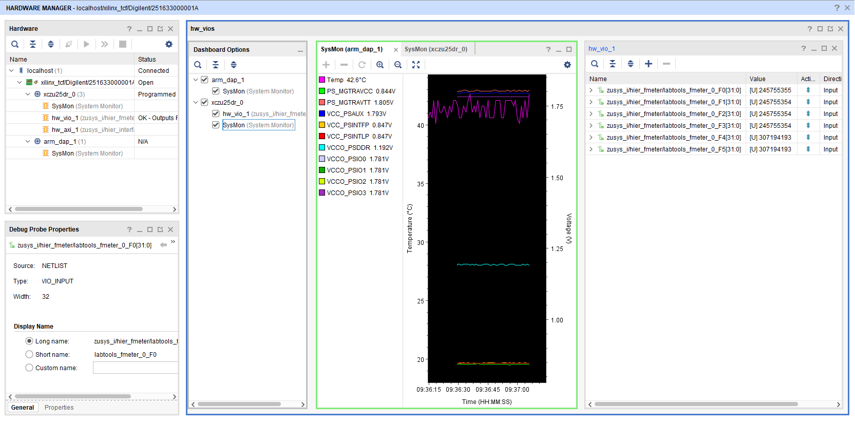
Open Vivado HW-Manager and add VIO signal to dashboard (*.ltx located on prebuilt folder)
- Monitoring:
- The output frequency of MMCM blocks can be monitored.
- Set radix from VIO signals to unsigned integer.
- The tempreature of ARM processor and FPGA can be measured too.
- The output frequency of MMCM blocks can be monitored.
| Scroll Title | ||||
|---|---|---|---|---|
| ||||
 |
Software Setup
Download RF Analyzer GUI from the following link and install it.
Hardware Setup
The Hardware contains of a TE0835 module and TEB0835 carrier board and has 8 ADC inputs and 8 DAC outputs.
- Plug the TE0835 module on the TEB0835 carrier board
- Install the cooler on the RFSoC
- Connect the micro USB cable to the J29 connector
- Plug the 12V power supply cable to the J19 connector
- Plug the prepared SD card on the SD card socket (J28)
- Connect a cable with SMA or UFL connector to one of the DAC connector( for example DAC0 J9) and feed it back to the related ADC input (for example ADC0 J1)
- (optional) A signal generator can be used to feed desired sinal to ADC input.
- (optional) An oscilloscope can be used to monitor the output signal of DAC.
| RF Analyzer GUI | ADC/DAC | Board | Designator | Pin Name | Pin Number | Connected with | Board | Pin Name | Designator | Footprint |
|---|---|---|---|---|---|---|---|---|---|---|
| ADC Tile 0 | ADC 01 | TE0835 | U1 | ADC0_P/ADC0_N | AK2/AK1 | B2B | TEB0835 | ADC0_P/ADC0_N | J1 | SMA |
| ADC Tile 0 | ADC 23 | TE0835 | U1 | ADC1_P/ADC1_N | AH2/AH1 | B2B | TEB0835 | ADC1_P/ADC1_N | J2 | UFL |
| ADC Tile 1 | ADC 01 | TE0835 | U1 | ADC2_P/ADC2_N | AF2/AF1 | B2B | TEB0835 | ADC2_P/ADC2_N | J3 | SMA |
| ADC Tile 1 | ADC 23 | TE0835 | U1 | ADC3_P/ADC3_N | AD2/AD1 | B2B | TEB0835 | ADC3_P/ADC3_N | J4 | UFL |
| ADC Tile 2 | ADC 01 | TE0835 | U1 | ADC4_P/ADC4_N | AB2/AB1 | B2B | TEB0835 | ADC4_P/ADC4_N | J5 | SMA |
| ADC Tile 2 | ADC 23 | TE0835 | U1 | ADC5_P/ADC5_N | Y2/Y1 | B2B | TEB0835 | ADC5_P/ADC5_N | J6 | UFL |
| ADC Tile 3 | ADC 01 | TE0835 | U1 | ADC6_P/ADC6_N | V2/V1 | B2B | TEB0835 | ADC6_P/ADC6_N | J7 | SMA |
| ADC Tile 3 | ADC 23 | TE0835 | U1 | ADC7_P/ADC7_N | T2/T1 | B2B | TEB0835 | ADC7_P/ADC7_N | J8 | UFL |
| DAC Tile 0 | DAC 0 | TE0835 | U1 | DAC0_P/DAC0_N | N2/N1 | B2B | TEB0835 | DAC0_P/DAC0_N | J9 | SMA |
| DAC Tile 0 | DAC 1 | TE0835 | U1 | DAC1_P/DAC1_N | L2/L1 | B2B | TEB0835 | DAC1_P/DAC1_N | J10 | UFL |
| DAC Tile 0 | DAC 2 | TE0835 | U1 | DAC2_P/DAC2_N | J2/J1 | B2B | TEB0835 | DAC2_P/DAC2_N | J11 | SMA |
| DAC Tile 0 | DAC 3 | TE0835 | U1 | DAC3_P/DAC3_N | G2/G1 | B2B | TEB0835 | DAC3_P/DAC3_N | J12 | UFL |
| DAC Tile 1 | DAC 0 | TE0835 | U1 | DAC4_P/DAC4_N | E2/E1 | B2B | TEB0835 | DAC4_P/DAC4_N | J13 | UFL |
| DAC Tile 1 | DAC 1 | TE0835 | U1 | DAC5_P/DAC5_N | C2/C1 | B2B | TEB0835 | DAC5_P/DAC5_N | J14 | UFL |
| DAC Tile 1 | DAC 2 | TE0835 | U1 | DAC6_P/DAC6_N | B4/A4 | B2B | TEB0835 | DAC6_P/DAC6_N | J15 | UFL |
| DAC Tile 1 | DAC 3 | TE0835 | U1 | DAC7_P/DAC7_N | B6/A6 | B2B | TEB0835 | DAC7_P/DAC7_N | J16 | UFL |
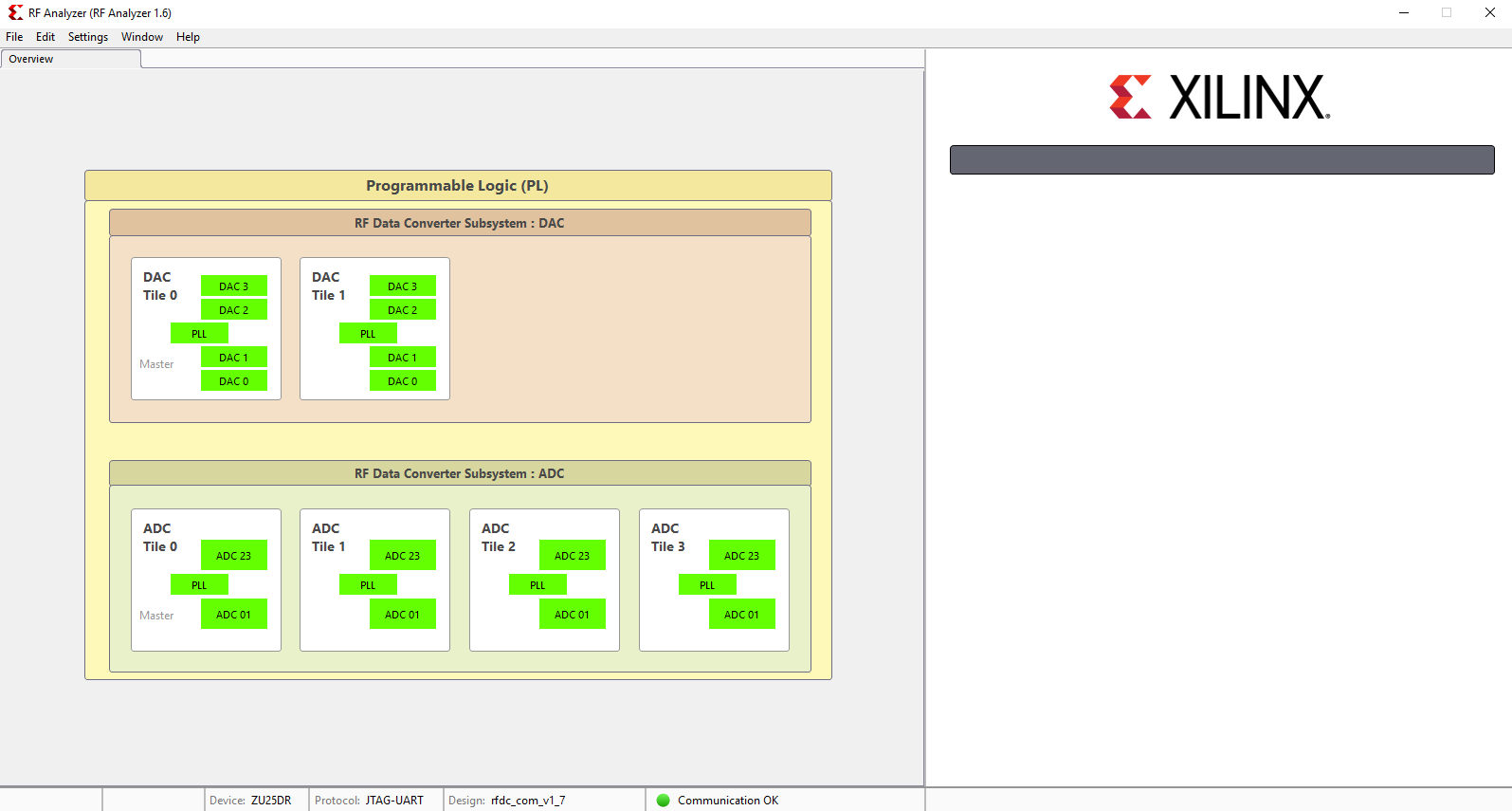
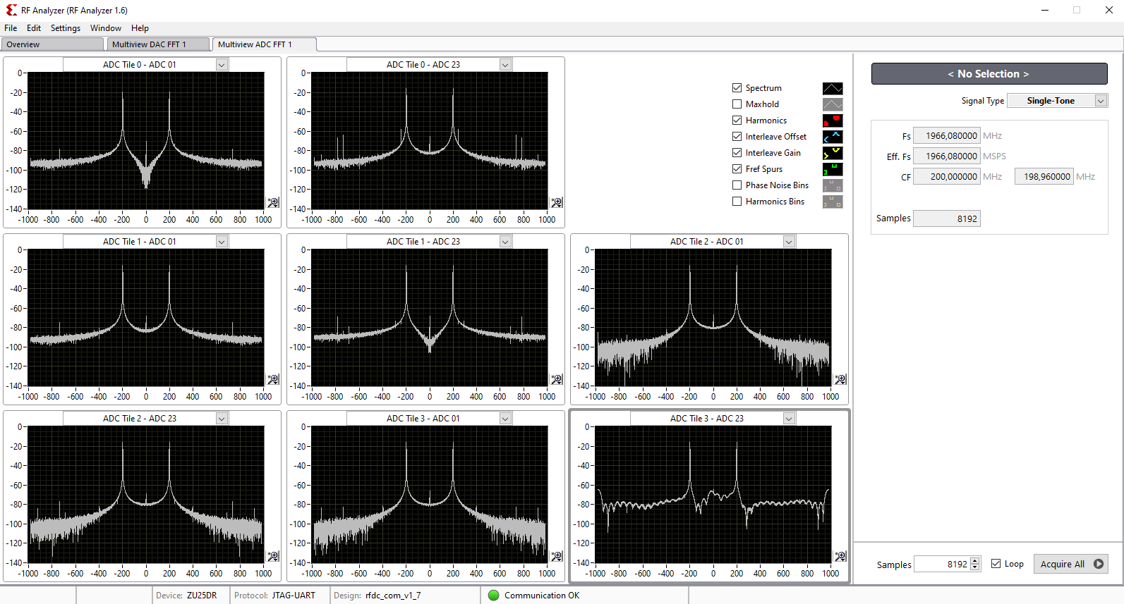
RF Analyzer
- Open the RF Analyzer GUI
- Click on Connect
- Adjust the desired JTAG frequency (for example 30MHZ)
- Give the generated bitstream file path
- Click on Download Bitstream on the FPGA
- When downloading is finished, click on Select Target
- After the initilalisation, all ADCs/DACs tiles are visible
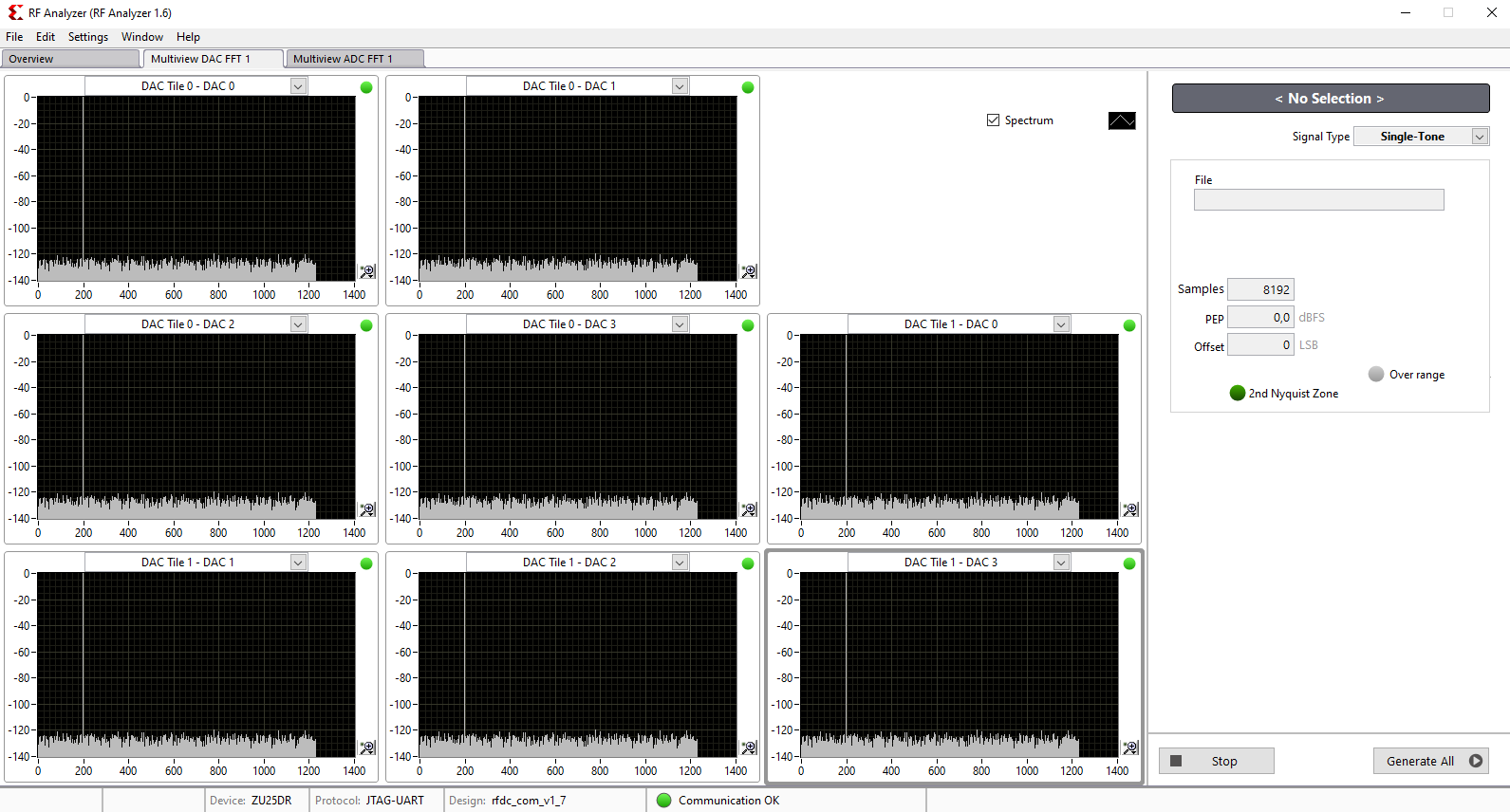
- Click on desired DAC tile and choose a DAC (for example DAC0)
- Adjust the desired DAC properties (for example output frequency)
- Click on Generate to generate the signal in output of DAC
- Click on the related ADC tile and choose the related ADC (for example ADC0)
- Click on Acquire to aqcuire the input signal
- The spectum of the DAC output signal can be seen now. The signal can be visible in time domain too.
- Tip: In menu Window click on Multiview to see all of DACs and ADCs simultaneously.
- Tip: In menu Window click on Multiview to see all of DACs and ADCs simultaneously.
| Expand | ||
|---|---|---|
| ||
|
| Expand | ||
|---|---|---|
| ||
|
| Expand | ||
|---|---|---|
| ||
|
TE Scripts are only needed to generate the vivado project, all other additional steps are optional and can also executed by Xilinx Vivado/SDK GUI. For currently Scripts limitations on Win and Linux OS see: Project Delivery Currently limitations of functionality
- _create_win_setup.cmd/_create_linux_setup.sh and follow instructions on shell:
- Press 0 and enter to start "Module Selection Guide"
- (optional Win OS) Generate Virtual Drive or use short directory for the reference design (for example x:\<design name>)
- Create Project (follow instruction of the product selection guide), settings file will be configured automatically during this process)
- (optional for manual changes) Select correct device and Xilinx install path on "design_basic_settings.cmd" and create Vivado project with "vivado_create_project_guimode.cmd"
Note: Select correct one, see alsoTE Board Part Files
- (optional for manual changes) Select correct device and Xilinx install path on "design_basic_settings.cmd" and create Vivado project with "vivado_create_project_guimode.cmd"
- Create XSA and export to prebuilt folder
- Run on Vivado TCL: TE::hw_build_design -export_prebuilt
Note: Script generate design and export files into \prebuilt\hardware\<short dir>. Use GUI is the same, except file export to prebuilt folder
- Run on Vivado TCL: TE::hw_build_design -export_prebuilt
- Create Linux (bl31.elf, uboot.elf and image.ub) with exported XSA
- XSA is exported to "prebuilt\hardware\<short name>"
Note: HW Export from Vivado GUI create another path as default workspace. - Create Linux images on VM, see PetaLinux KICKstart
- Use TE Template from /os/petalinux
- XSA is exported to "prebuilt\hardware\<short name>"
- Add Linux files (bl31.elf, uboot.elf and image.ub) to prebuilt folder
- "prebuilt\os\petalinux\<ddr size>" or "prebuilt\os\petalinux\<short name>"
- Generate Programming Files with Vitis
- Run on Vivado TCL: TE::sw_run_vitis -all
Note: Scripts generate applications and bootable files, which are defined in "sw_lib\apps_list.csv" - (alternative) Start SDK with Vivado GUI or start with TE Scripts on Vivado TCL: TE::sw_run_vitis
Note: TCL scripts generate also platform project, this must be done manuelly in case GUI is used. See Vitis
- Run on Vivado TCL: TE::sw_run_vitis -all
Launch
| Page properties | ||||
|---|---|---|---|---|
| ||||
Note:
|
Programming
| Note |
|---|
Check Module and Carrier TRMs for proper HW configuration before you try any design. |
Xilinx documentation for programming and debugging: Vivado/SDK/SDSoC-Xilinx Software Programming and Debugging
Get prebuilt boot binaries
- _create_win_setup.cmd/_create_linux_setup.sh and follow instructions on shell
- Press 0 and enter to start "Module Selection Guide"
- Select assembly version
- Validate selection
- Select Create and open delivery binary folder
Note: Folder (<project foler>/_binaries_<Artikel Name>) with subfolder (boot_<app name>) for different applications will be generated
QSPI
Optional for Boot.bin on QSPI Flash and image.ub on SD.
- Connect JTAG and power on carrier with module
- Open Vivado Project with "vivado_open_existing_project_guimode.cmd" or if not created, create with "vivado_create_project_guimode.cmd"
- Type on Vivado TCL Console: TE::pr_program_flash -swapp u-boot
Note: To program with SDK/Vivado GUI, use special FSBL (zynqmp_fsbl_flash) on setup
optional "TE::pr_program_flash -swapp hello_te0835" possible - Copy image.ub on SD-Card
- use files from (<project foler>/_binaries_<Articel Name>)/boot_linux from generated binary folder,see: Get prebuilt boot binaries
- or use prebuilt file location, see <design_name>/prebuilt/readme_file_location.txt
- Insert SD-Card
SD
- Copy image.ub and Boot.bin on SD-Card
- use files from (<project foler>/_binaries_<Articel Name>)/boot_linux from generated binary folder,see: Get prebuilt boot binaries
- or use prebuilt file location, see <design_name>/prebuilt/readme_file_location.txt
- Set Boot Mode to SD-Boot.
- Depends on Carrier, see carrier TRM.
- Insert SD-Card in SD-Slot.
JTAG
Not used on this Example.
Usage
- Prepare HW like described on section TE0835 Test Board#Hardware Setup
- Connect UART USB (most cases same as JTAG)
- Select SD Card as Boot Mode (or QSPI - depending on step 1)
Note: See TRM of the Carrier, which is used. - Power On PCB
Note: 1. Zynqmp RFSoC Boot ROM loads FSBL from SD into OCM, 2. FSBL loads U-boot from SD into DDR, 3. U-boot load Linux from SD into DDR - Open the RF Analyzer GUI
- Click on Connect
- Adjust the desired JTAG frequency (for example 30MHZ)
- Give the generated bitstream file path
- Click on Download Bitstream on the FPGA
- When downloading is finished, click on Select Target
- After the initilalisation, all ADCs/DACs tiles are visible
- Click on desired DAC tile and choose a DAC (for example DAC0)
- Adjust the desired DAC properties (for example output frequency)
- Click on Generate to generate the signal in output of DAC
- Click on the related ADC tile and choose the related ADC (for example ADC0)
- Click on Acquire to aqcuire the input signal
- The spectum of the DAC output signal can be seen now. The signal can be visible in time domain too.
- Tip: In menu Window click on Multiview to see all of DACs and ADCs simultaneously.
| Expand | ||
|---|---|---|
| ||
|
| Expand | ||
|---|---|---|
| ||
|
| Expand | ||
|---|---|---|
| ||
|
Linux
- Open Serial Console (e.g. putty)
- Speed: 115200
- COM Port: Win OS, see device manager, Linux OS see dmesg |grep tty (UART is *USB1)
- Linux Console:
Note: Wait until Linux boot finished For Linux Login use:- User Name: root
- Password: root
- You can use Linux shell now.
- I2C 0 Bus type: i2cdetect -y -r 0
- I2C 1 Bus type: i2cdetect -y -r 1
- RTC check: dmesg | grep rtc
- ETH0 works with udhcpc
- USB type "lsusb" or connect USB2.0 device
- Option Features
- Webserver to get access to Zynqmp RFSoC
- insert IP on web browser to start web interface
- init.sh scripts
- add init.sh script on SD, content will be load automatically on startup (template included in ./misc/SD)
- add init.sh script on SD, content will be load automatically on startup (template included in ./misc/SD)
- Webserver to get access to Zynqmp RFSoC
Vivado HW Manager
| Page properties | ||||
|---|---|---|---|---|
| ||||
Note:
|
Open Vivado HW-Manager and add VIO signal to dashboard (*.ltx located on prebuilt folder)
- Monitoring:
- The output frequency of MMCM blocks can be monitored.
- Set radix from VIO signals to unsigned integer.
- The tempreature of ARM processor and FPGA can be measured too.
- The output frequency of MMCM blocks can be monitored.
| Scroll Title | ||||
|---|---|---|---|---|
| ||||
|
System Design - Vivado
| Page properties | ||||
|---|---|---|---|---|
| ||||
Note:
|
...
Overview
Content Tools