Page History
...
- Plug the TE0835 module on the TEB0835 carrier board
- Install the cooler on the RFSoC
- Connect the micro USB cable to the J29 connector
- Plug the 12V power supply cable to the J19 connector
- Plug the prepared SD card on the SD card socket (J28)
- Connect a cable with SMA or UFL connector to one of the DAC connector( for example DAC0 J9) and feed it back to the related ADC input (for example ADC0 J1)
- (optional) A signal generator can be used to feed desired sinal to ADC input.
- (optional) An oscilloscope can be used to monitor the output signal of DAC.
| RF Analyzer GUI | ADC/DAC | Board | Designator | Pin Name | Pin Number | Connected with | Board | Pin Name | Designator | Footprint |
|---|---|---|---|---|---|---|---|---|---|---|
| ADC Tile 0 | ADC 01 | TE0835 | U1 | ADC0_P/ADC0_N | AK2/AK1 | B2B | TEB0835 | ADC0_P/ADC0_N | J1 | SMA |
| ADC Tile 0 | ADC 23 | TE0835 | U1 | ADC1_P/ADC1_N | AH2/AH1 | B2B | TEB0835 | ADC1_P/ADC1_N | J2 | UFL |
| ADC Tile 1 | ADC 01 | TE0835 | U1 | ADC2_P/ADC2_N | AF2/AF1 | B2B | TEB0835 | ADC2_P/ADC2_N | J3 | SMA |
| ADC Tile 1 | ADC 23 | TE0835 | U1 | ADC3_P/ADC3_N | AD2/AD1 | B2B | TEB0835 | ADC3_P/ADC3_N | J4 | UFL |
| ADC Tile 2 | ADC 01 | TE0835 | U1 | ADC4_P/ADC4_N | AB2/AB1 | B2B | TEB0835 | ADC4_P/ADC4_N | J5 | SMA |
| ADC Tile 2 | ADC 23 | TE0835 | U1 | ADC5_P/ADC5_N | Y2/Y1 | B2B | TEB0835 | ADC5_P/ADC5_N | J6 | UFL |
| ADC Tile 3 | ADC 01 | TE0835 | U1 | ADC6_P/ADC6_N | V2/V1 | B2B | TEB0835 | ADC6_P/ADC6_N | J7 | SMA |
| ADC Tile 3 | ADC 23 | TE0835 | U1 | ADC7_P/ADC7_N | T2/T1 | B2B | TEB0835 | ADC7_P/ADC7_N | J8 | UFL |
| DAC Tile 0 | DAC 0 | TE0835 | U1 | DAC0_P/DAC0_N | N2/N1 | B2B | TEB0835 | DAC0_P/DAC0_N | J9 | SMA |
| DAC Tile 0 | DAC 1 | TE0835 | U1 | DAC1_P/DAC1_N | L2/L1 | B2B | TEB0835 | DAC1_P/DAC1_N | J10 | UFL |
| DAC Tile 0 | DAC 2 | TE0835 | U1 | DAC2_P/DAC2_N | J2/J1 | B2B | TEB0835 | DAC2_P/DAC2_N | J11 | SMA |
| DAC Tile 0 | DAC 3 | TE0835 | U1 | DAC3_P/DAC3_N | G2/G1 | B2B | TEB0835 | DAC3_P/DAC3_N | J12 | UFL |
| DAC Tile 1 | DAC 0 | TE0835 | U1 | DAC4_P/DAC4_N | E2/E1 | B2B | TEB0835 | DAC4_P/DAC4_N | J13 | UFL |
| DAC Tile 1 | DAC 1 | TE0835 | U1 | DAC5_P/DAC5_N | C2/C1 | B2B | TEB0835 | DAC5_P/DAC5_N | J14 | UFL |
| DAC Tile 1 | DAC 2 | TE0835 | U1 | DAC6_P/DAC6_N | B4/A4 | B2B | TEB0835 | DAC6_P/DAC6_N | J15 | UFL |
| DAC Tile 1 | DAC 3 | TE0835 | U1 | DAC7_P/DAC7_N | B6/A6 | B2B | TEB0835 | DAC7_P/DAC7_N | J16 | UFL |
RF Analyzer
- Open the RF Analyzer GUI
- Click on Connect
- Adjust the desired JTAG frequency (for example 30MHZ)
- Give the generated bitstream file path
- Click on Download Bitstream on the FPGA
- When downloading is finished, click on Select Target
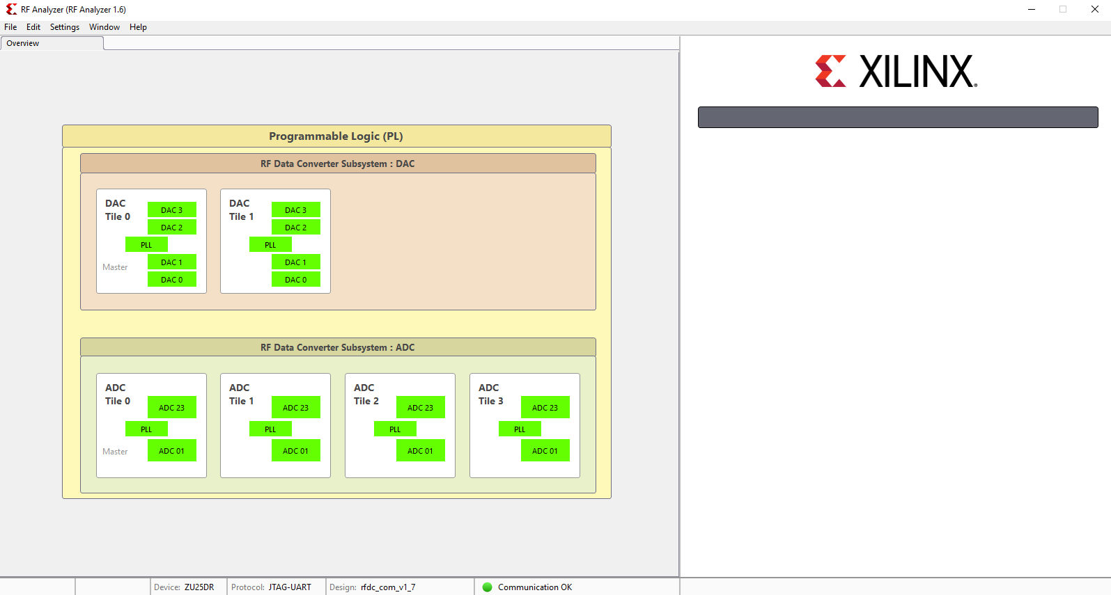
- After the initilalisation, all ADCs/DACs tiles are visible
- Click on desired DAC tile and choose a DAC (for example DAC0)
- Adjust the desired DAC properties (for example output frequency)
- Click on Generate to generate the signal in output of DAC
- Click on the related ADC tile and choose the related ADC (for example ADC0)
- Click on Acquire to aqcuire the input signal
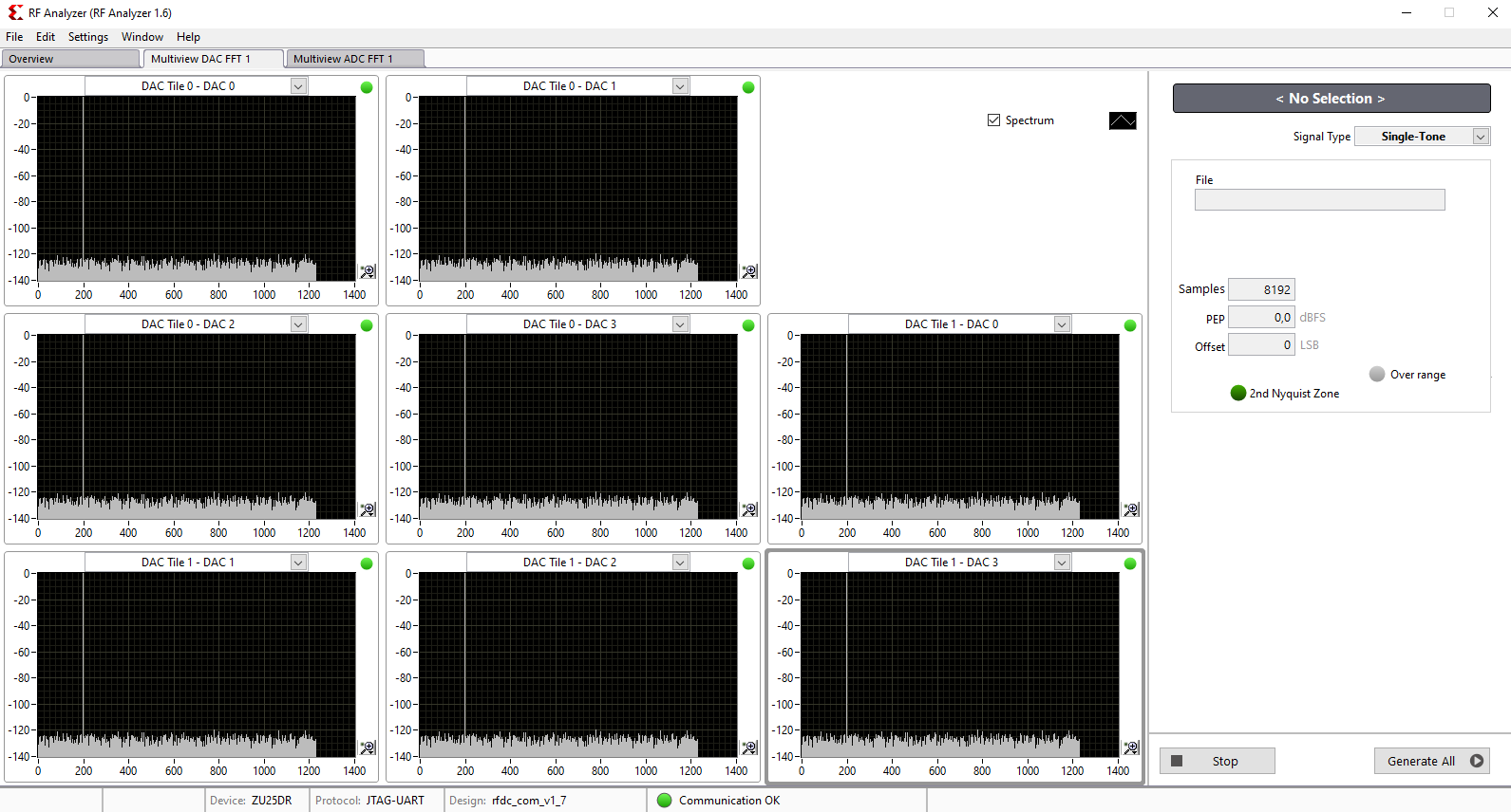
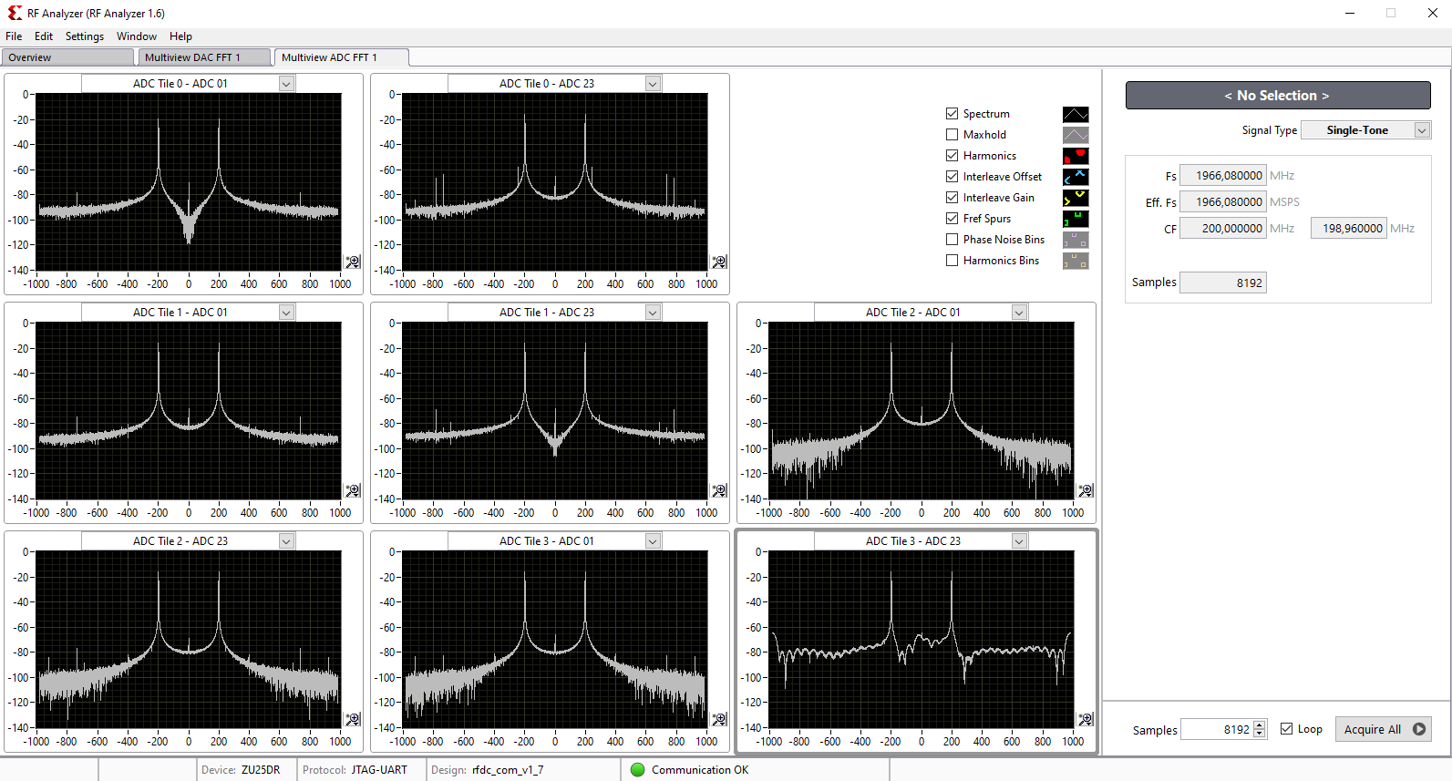
- The spectum of the DAC output signal can be seen now. The signal can be visible in time domain too.
- Tip: In menu Window click on Multiview to see all of DACs and ADCs simultaneously.
- Tip: In menu Window click on Multiview to see all of DACs and ADCs simultaneously.
| Scroll Title | |||
|---|---|---|---|
| |||
| |||
 | |||
| Scroll Title | ||||
|---|---|---|---|---|
| ||||
 |
| Scroll Title | |||
|---|---|---|---|
| |||
| |||
 |
System Design - Vivado
| Page properties | ||||
|---|---|---|---|---|
| ||||
Note:
|
...
Overview
Content Tools