...
| Excerpt |
|---|
- Vitis/Vivado 2019.2
- PetaLinux
- RF Analyzer 1.6
- PCIe (endpoint)
- SD
- ETH
- USB
- I2C
- RTC
- FMeter
- Modified FSBL for SI5395 programming
- Special FSBL for QSPI programming
|
...
| Scroll Title |
|---|
| anchor | Table_AHW |
|---|
| title | Additional Hardware |
|---|
|
| Scroll Table Layout |
|---|
| orientation | portrait |
|---|
| sortDirection | ASC |
|---|
| repeatTableHeaders | default |
|---|
| style | |
|---|
| widths | |
|---|
| sortByColumn | 1 |
|---|
| sortEnabled | false |
|---|
| cellHighlighting | true |
|---|
|
| Additional Hardware | Notes |
|---|
| Micro USB Cable for JTAG/UART |
| | Cooler | It's recommended to use cooler on Zynqmp RFSoC device | | SMA male connector cable | Some ADC inputs/DAC outouts have the SMA connector | | UFL female connector cable | Some ADC inputs/DAC outouts have the UFL connector | | Ethernet cable |
| | SD card | 16GB | | Signal generator (optional) | To feed a desired signal to the input of ADC | | Oscilloscope (optional) | To monitor the output signal of DACs. | | PC | with ATX Powrer supply and PCIe X? slot | 12V power supply | It is recommended to use a power supply with 3A output current capability |
|
Content
...
Software Setup
Download RF Analyzer GUI from the following link and install it.
Design Flow
...
JTAG
Not used on this Example.
Usage
.
Hardware Setup
The Hardware contains of a TE0835 module and TEB0835 carrier board and has 8 ADC inputs and 8 DAC outputs.
- Plug the TE0835 module on the TEB0835 carrier board
- Install the cooler on the RFSoC
- Connect the micro USB cable to the J29 connector
- Plug the 12V power supply cable to the J19 connector
- Plug the prepared SD card on the SD card socket (J28)
- Connect a cable with SMA or UFL connector to one of the DAC connector( for example DAC0 J9) and feed it back to the related ADC input (for example ADC0 J1)
- (optional) A signal generator can be used to feed desired sinal to ADC input.
- (optional) An oscilloscope can be used to monitor the output signal of DAC.
Usage
- Prepare HW like described on section TE0835 Test Board#Hardware Setup
- Connect UART USB (most cases
- Prepare HW like described on section TE0835 Test Board#Hardware Setup
- Connect UART USB (most cases same as JTAG)
- Select SD Card as Boot Mode (or QSPI - depending on step 1)
Note: See TRM of the Carrier, which is used. - Power On PCB
Note: 1. Zynqmp RFSoC Boot ROM loads FSBL from SD into OCM, 2. FSBL loads U-boot from SD into DDR, 3. U-boot load Linux from SD into DDR
...
- Open Serial Console (e.g. putty)
- Speed: 115200
- COM Port: Win OS, see device manager, Linux OS see dmesg |grep tty (UART is *USB1)
- Linux Console:
Note: Wait until Linux boot finished For Linux Login use:
- User Name: root
- Password: root
- You can use Linux shell now.
- I2C 0 Bus type: i2cdetect -y -r 0
I2C 1 Bus type: i2cdetect -y -r 1- Bus 0 up to 5 possible
- RTC check: dmesg | grep rtc
- ETH0 works with udhcpc
- USB type "lsusb" or connect USB2.0 device
- PCIe Bus type: "lspci"
- PCIe device should be seen in the console
- Option Features
- Webserver to get access to Zynqmp RFSoC
- insert IP on web browser to start web interface
- init.sh scripts
- add init.sh script on SD, content will be load automatically on startup (template included in ./misc/SD)
...
| Scroll Title |
|---|
| anchor | Figure_VHM |
|---|
| title | Vivado Hardware Manager |
|---|
|
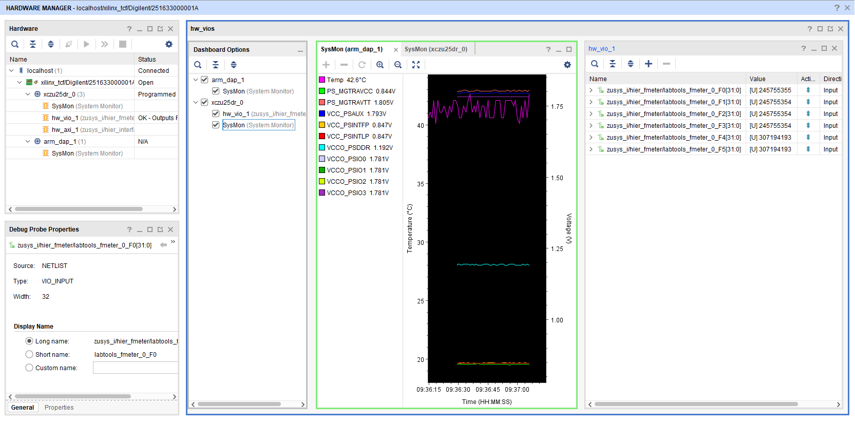 |
...
...
RF Analyzer
...
- Open the RF Analyzer GUI
Hardware Setup
The Hardware contains of a TE0835 module and TEB0835 carrier board and has 8 ADC inputs and 8 DAC outputs.
- Plug the TE0835 module on the TEB0835 carrier board
- Install the cooler on the RFSoC
- Connect the micro USB cable to the J29 connector
- Plug the 12V power supply cable to the J19 connector
- Plug the prepared SD card on the SD card socket (J28)
- Connect a cable with SMA or UFL connector to one of the DAC connector( for example DAC0 J9) and feed it back to the related ADC input (for example ADC0 J1)
- (optional) A signal generator can be used to feed desired sinal to ADC input.
- (optional) An oscilloscope can be used to monitor the output signal of DAC.
- Click on Connect
- Adjust the desired JTAG frequency (for example 30MHZ)
- Give the generated bitstream file path
- Click on Download Bitstream on the FPGA
- When downloading is finished, click on Select Target
- After the initilalisation, all ADCs/DACs tiles are visible
- Click on desired DAC tile and choose a DAC (for example DAC0)
- Adjust the desired DAC properties (for example output frequency)
- Click on Generate to generate the signal in output of DAC
- Click on the related ADC tile and choose the related ADC (for example ADC0)
- Click on Acquire to aqcuire the input signal
- The spectum of the DAC output signal can be seen now. The signal can be visible in time domain too.
- Tip: In menu Window click on Multiview to see all of DACs and ADCs simultaneously.
| RF Analyzer GUI | Board TE0835 ( RFSoC U1) |
| TEB0835 |
|---|
| Tile | ADC/DAC | SoC Pin Name | SoC Pin Number | B2B | Signal Name | Connector Designator | Connector Type |
|---|
RF Analyzer GUI | ADC/DAC | Board | Designator | Pin Name | Pin Number | Connected with | Board | Pin Name | Designator | FootprintTE0835 | U1TEB0835 | ADC0_P/ADC0_N | J1 | SMA |
| ADC Tile 0 | ADC 23 |
TE0835 | U1TEB0835 | ADC1_P/ADC1_N | J2 | UFL |
| ADC Tile 1 | ADC 01 |
TE0835 | U1TEB0835 | ADC2_P/ADC2_N | J3 | SMA |
| ADC Tile 1 | ADC 23 |
TE0835 | U1 | TEB0835 | ADC3_P/ADC3_N | J4 | UFL |
| ADC Tile 2 | ADC 01 |
TE0835 | U1TEB0835 | ADC4_P/ADC4_N | J5 | SMA |
| ADC Tile 2 | ADC 23 |
TE0835 | U1TEB0835 | ADC5_P/ADC5_N | J6 | UFL |
| ADC Tile 3 | ADC 01 |
TE0835 | U1TEB0835 | ADC6_P/ADC6_N | J7 | SMA |
| ADC Tile 3 | ADC 23 |
TE0835 | U1TEB0835 | ADC7_P/ADC7_N | J8 | UFL |
| DAC Tile 0 | DAC 0 |
TE0835U1 | TEB0835 | DAC0_P/DAC0_N | J9 | SMA |
| DAC Tile 0 | DAC 1 |
TE0835 | U1TEB0835 | DAC1_P/DAC1_N | J10 | UFL |
| DAC Tile 0 | DAC 2 |
TE0835 | U1TEB0835 | DAC2_P/DAC2_N | J11 | SMA |
| DAC Tile 0 | DAC 3 |
TE0835 | U1 | TEB0835 | DAC3_P/DAC3_N | J12 | UFL |
| DAC Tile 1 | DAC 0 |
TE0835U1 | TEB0835 | DAC4_P/DAC4_N | J13 | UFL |
| DAC Tile 1 | DAC 1 |
TE0835 | U1 | TEB0835 | | DAC5_P/DAC5_N | J14 | UFL |
| DAC Tile 1 | DAC 2 |
TE0835 | U1TEB0835 | DAC6_P/DAC6_N | J15 | UFL |
| DAC Tile 1 | DAC 3 |
TE0835U1 | TEB0835 | ...
| Scroll Title |
|---|
| anchor | Figure_VHM |
|---|
| title | Overview |
|---|
|
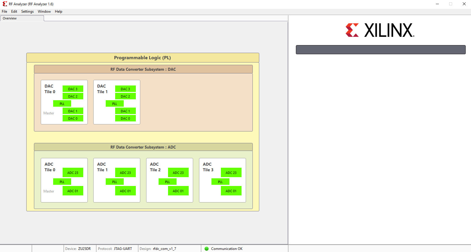 |
...