Page History
...
| Name / opt. VHD Name | Direction | Pin | Pullup/Down | Bank Power | Description |
|---|---|---|---|---|---|
| BOOT_R / BOOTMODE_R | out | N12 | NONE | 3.3V | If low then the QSPI flash can not be written. (Write protect) |
| BOOT_R5 / BOOTMODE_R5 | out | M11 | DOWN | 3.3V | If low then the QSPI flash will be reset. (HOLD/RESET) |
| CLK_125MHz | in | G13 | NONE | 1.8V | 125MHZ Clock Output of Ethernet transceiver chip (88E1512-A0-NNP2C000) that synchronized with the 25MHZ reference clock |
| EN_3V3 | out | A2 | DOWN | 3.3V | If high then the 3.3V power will be switched ON. |
| EN1 | in | A9 | UP | 3.3V | User Enable. Enables the DC-DC converters and on board supplies (Active High). (B2B JM1-28)(DIP Switch on the carrier board) . Not used if NOSEQ = '1' |
| ETH-CLK-EN / EN_ETH_CLK | out | J14 | NONE | 1.8V | Enable pin for U9 oscillator chip U9 (SiT8008BI-73-18S-25.000000E) to feed a clock to Ethernet Transceiver(U8). Enabled as default. |
| ETH-MDC / mdc | in | L14 | UP | 1.8V | Management Data Clock reference for the Ethernet transceiver chip. This pin is connected with MIO52 of FPGA too and can be activated in Zynq7 adjustment. |
| ETH-MDIO / mdio | inout | K14 | UP | 1.8V | It is Management Data pin of Ethernet transceiver chip to transfer in and out of the device synchronously to mdc. It is connected with MIO53 of FPGA. |
| ETH-RST | out | E14 | DOWN | 1.8V | Reset pin of Ethernet transceiver chip. (Active low) |
| INIT | in | C9 | UP | 3.3V | INIT_B_0 pin of FPGA. (Active low). This pin must be tristate for PL configuratuion. By user or device held low until is ready to be configured. |
| INT1 / INT2 | in | P4 | UP | 3.3V | MEMS Interrupt 1 of 3D accelerometer and 3D magnetometer chip U22 (LSM303DTR) (Active High) |
| INT2 / INT1 | in | P6 | UP | 3.3V | MEMS Interrupt 2 of 3D accelerometer and 3D magnetometer chip U22 (LSM303DTR) (Active High) |
| JTAGMODE | in | B9 | 3.3V | Enable JTAG access to CPLD for Firmware update (zero: JTAG routed to module, one: CPLD access) | |
| LED1 | out | P2 | NONE | 3.3V | Display green LED (D2) |
| LED2 | out | N3 | DOWN | 3.3V | Display red LED (D5) |
| MEM-MAC / MAC_IO | inout | M14 | UP | 1.8V | Serial Clock/Data input/Output of Serial EEPROM (11AA02E48T-I/TT) U17 |
| MEM-SHA / SHA_IO | inout | N14 | UP | 1.8V | SDA for CryptoAuthentication Chip (ATSHA204A-STUCZ-T) U10 |
| MIO14 | inout | M4 | NONE | 3.3V | RX pin of UART0 |
| MIO15 | inout | N4 | NONE | 3.3V | TX pin of UART0 |
| MIO7 | in | P11 | UP | 3.3V | This pin is used as GPIO. |
| MMC_RST | out | G14 | DOWN | 1.8V | Reset pin of eMMC memory (MTFC16GJVEC-2M WT) U15 |
| MODE / BOOTMODE_IN | in | C8 | UP | 3.3V | Latched as BOOTMODE once at power-up, can be used later as I/O, weak pull up. Force low for boot from the SD Card. Latched at power on only, not on soft reset (B2B-JM1 pin 32) |
| MODE / BOOTMODE_IN2 | in | M9 | UP | 3.3V | Latched as BOOTMODE once at power-up, can be used later as I/O, weak pull up. Force low for boot from the SD Card. Latched at power on only, not on soft reset (B2B-JM1 pin 32) |
| MR / POR_B | out | P12 | UP | 3.3V | Power-on-reset pin. This pin is connected with supply voltage monitor chip (TPS3106K33DBVR) U26 and controls the PS_POR_B pin of FPGA. (Active Low) |
| NetU19_B12 | B12 | / currently_not_used | |||
| NetU19_B13 | B13 | / currently_not_used | |||
| NetU19_B2 | B2 | / currently_not_used | |||
| NetU19_B3 | B3 | / currently_not_used | |||
| NetU19_B7 | B7 | / currently_not_used | |||
| NetU19_C1 | C1 | / currently_not_used | |||
| NetU19_C10 | C10 | / currently_not_used | |||
| NetU19_C12 / Dummy | out | C12 | DOWN | 3.3V | |
| NetU19_C3 | C3 | / currently_not_used | |||
| NetU19_C6 / RST | in | C6 | UP | 3.3V | |
| NetU19_C7 | C7 | / currently_not_used | |||
| NetU19_E1 | E1 | / currently_not_used | |||
| NetU19_E12 | E12 | / currently_not_used | |||
| NetU19_F13 | F13 | / currently_not_used | |||
| NetU19_F3 | F3 | / currently_not_used | |||
| NetU19_G3 | G3 | / currently_not_used | |||
| NetU19_H3 | H3 | / currently_not_used | |||
| NetU19_J3 | J3 | / currently_not_used | |||
| NetU19_K13 | K13 | / currently_not_used | |||
| NetU19_K3 | K3 | / currently_not_used | |||
| NetU19_L3 | L3 | / currently_not_used | |||
| NetU19_M12 | M12 | / currently_not_used | |||
| NetU19_M2 | M2 | / currently_not_used | |||
| NetU19_M3 | M3 | / currently_not_used | |||
| NetU19_N13 | N13 | / currently_not_used | |||
| NetU19_N5 | N5 | / currently_not_used | |||
| NetU19_N7 | N7 | / currently_not_used | |||
| NetU19_N8 | N8 | / currently_not_used | |||
| NOSEQ | inout | A3 | DOWN | 3.3V | Usage CPLD Variant depends. (B2B-NOSEQ pin 7) Forces the 1.0V and 1.8V DC-DC converters always ON when high. Can be used as an I/O after boot. |
| ON_1V0 | out | A12 | NONE | 3.3V | Enable pin for 1.0 V DC-DC (Active High) |
| ON_1V5 | out | M7 | NONE | 3.3V | Enable pin for 1.5 V DC-DC (Active High) |
| ON_1V8 | out | A11 | NONE | 3.3V | Enable pin for 1.8 V DC-DC (Active High) |
| OTG-RST | out | B14 | DOWN | 1.8V | Reset pin for high speed USB transceiver (USB3320C-EZK) U18 (Active Low) |
| PG_1V0 | in | A7 | UP | 3.3V | Power OK (POK) pin of 1.0V DC-DC converter EN6347QI (U1). If High then the output voltage of regulator is within 10% of nominal value (OK). |
| PG_1V5 | in | N6 | UP | 3.3V | Power OK (POK) pin of 1.5V DC-DC converter EP53F8QI (U2). If High then the output voltage of regulator is Ok. |
| PG_1V8 | in | A10 | UP | 3.3V | Power OK (POK) pin of 1.8V DC-DC converter EP53F8QI (U3). If High then the output voltage of regulator is Ok. |
| PG_3V3 / POR | in | C11 | UP | 3.3V | POR Reset pin. This pin is connected with PG_3V3. As long as the VCCIO34 voltage is zero, this pin will remain low. |
| PGOOD | inout | B8 | UP | 3.3V | Power good output as default, can be used as I/O. (B2B JM1-Pin 30) Forced low until all on-board power supplies are working properly. |
| PHY_CONFIG | inout | C14 | DOWN | 1.8V | Hardware configuration pin of Ethernet transceiver (88E1512-A0-NNP2C000). |
| PHY_LED0 | inout | F14 | NONE | 1.8V | LED output 0 of Ehternet transceiver chip |
| PHY_LED1 | inout | D12 | NONE | 1.8V | LED output 1 of Ehternet transceiver chip |
| PHY_LED2 | inout | C13 | NONE | 1.8V | LED output 2 or interrupt output pin (Active Low) of Ehternet transceiver chip |
| PJTAG_R | out | N10 | NONE | 3.3V | This pin in the schematic is connected with SPI-DQ0/M0 Pin |
| PROG_B | in | A13 | UP | 3.3V | By pulsing this pin any configuration that is currently loaded is cleared and the PL prepared to load new configuration. (Active Low) |
| PS-RST / SRST_B | out | M13 | UP | 1.8V | PS software reset (Active Low) |
| PUDC_B | inout | E3 | DOWN | VCCIO34 | Selects the enable or disable of pull-ups during configuration on the user I/O pins. (Active Low) Enables internal pull-up resistors on the select I/O pins after power-up and during configuration. |
| RESIN | in | C4 | UP | 3.3V | Master reset input (Active Low). Default mapping forces POR_B reset to Zynq PS |
| RST / RST_SENSE | in | P3 | NONE | 3.3V | Reset pin that is connected with PS_PORT_B (Power-on-reset) (Active Low) |
| RTC_INT | in | N2 | UP | 3.3V | Interrupt output or frequency output of RTC chip (ISL12020MIRZ) U20 (Active Low) |
| SCL | inout | P8 | UP | 3.3V | I2C clock pin of MEMS chip (LSM303DTR) U22 |
| SDA | inout | P7 | UP | 3.3V | I2C data pin of MEMS chip (LSM303DTR) U22 |
| SPK_L | M5 | / currently_not_used | |||
| SPK_R | M8 | / currently_not_used | |||
| TCK / C_TCK | out | P13 | DOWN | 3.3V | Zynq JTAG clock pin |
| TDI / C_TDI | out | P9 | DOWN | 3.3V | Zynq JTAG data input pin |
| TDO / C_TDO | in | M10 | DOWN | 3.3V | Zynq JTAG data output pin |
| TMS / C_TMS | out | N9 | DOWN | 3.3V | Zynq JTAG mode select pin |
| VCCIO34 | E2 | / currently_not_used | |||
| VCCIO34 | F2 | / currently_not_used | |||
| VCCIO34 | H2 | / currently_not_used | |||
| VCCIO34 | J2 | / currently_not_used | |||
| VCCIO34 | K2 | / currently_not_used | |||
| X_TCK / M_TCK | in | B6 | DOWN | 3.3V | FTDI JTAG clock pin (B2B-JM1-pin 99) |
| X_TDI / M_TDI | in | B4 | DOWN | 3.3V | FTDI JTAG data input pin (B2B-JM1-pin 95) |
| X_TDO / M_TDO | out | A4 | DOWN | 3.3V | FTDI JTAG data output pin (B2B-JM1-pin 97) |
| X_TMS / M_TMS | in | A6 | DOWN | 3.3V | FTDI JTAG mode select pin (B2B-JM1-pin 93) |
| X1 | in | F1 | UP | VCCIO34 | CPLD pin to the FPGA (L16). I2C clock from FPGA |
| X2 / XIO4 | inout | C2 | UP | VCCIO34 | CPLD pin to the FPGA (M15). ETH PHY LED0 |
| X3 / XIO5 | inout | B1 | UP | VCCIO34 | CPLD pin to the FPGA (N15). ETH PHY LED1 |
| X4 / XIO6 | inout | D1 | UP | VCCIO34 | CPLD pin to the FPGA (P16). ETH PHY LED2 |
| X5 | out | J1 | NONE | VCCIO34 | CPLD pin to the FPGA (P22). I2C data to FPGA |
| X6 | H1 | / currently_not_used | |||
| X7 | in | M1 | UP | VCCIO34 | CPLD pin to the FPGA (N22). I2C data from FPGA |
| XCLK | out | K1 | NONE | VCCIO34 | CPLD pin to the FPGA (K19). ETH PHY clock to FPGA |
| - / SIG1 | in | E13 | NONE | 1.8V | This pin is connected with VCCIO34 directly in the schematic REV03 and has no lable in the schematic. |
SC B2B Pins
| Name | B2B | Mode | Default function | Alternative | Description |
|---|---|---|---|---|---|
| EN1 | JM1-Pin 28 | input, weak pull-up | Power Enable | IO | High enables the DC-DC converters and on-board supplies. Not used if NOSEQ=1 |
| MODE | JM1-Pin 32 | input, weak pull-up | Boot mode | SDA or IO | Force low for boot from the SD Card. Latched at power on only, not on soft reset! |
| NOSEQ | JM1-Pin 7 | input, weak pull-down | Power sequencing Control | Output | Forces the 1.0V and 1.8V DC-DC converters always ON when high. Can be used as an I/O after boot. |
| PGOOD | JM1-Pin 30 | output, open drain | Power good | SCL or IO | Forced low until all on-board power supplies are working properly. Attention: During CPLD programming, this pins is high impedance. |
| RESIN | JM2-Pin 18 | input, weak pull-up | Reset input | IO | Active Low Reset input, default mapping forces POR_B reset to Zynq PS |
NOSEQ Pin
This is a dedicated input that forces the module's 1.0V and 1.8V supplies to be enabled if high. This pin has a weak pull-down on the module. If left open the module will power up in normal power sequencing enabled mode. This pin is 3.3V tolerant. This pin is also connected to the System Management Controller. The SC can read the status of this pin (that is it can detect if the module is in power sequencing enabled mode). The SC can also use this pin as output after normal power on sequence. Please check the SC description for the function. SC rev 0.02 maps Ethernet PHY LED0 to NOSEQ by default (the mapping can be changed by software after boot).
...
NOSEQ can be used as an output after boot. NOSEQ must be low when 3.3V power is applied to the module. Common usage is an LED connected between NOSEQ and GND.
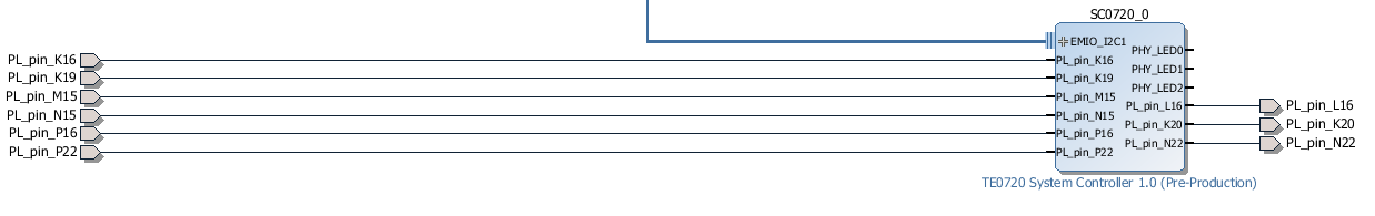
SC Pins to the FPGA
| Schematic net name | Default function | Direction | SC pin | FPGA pin | Description |
|---|---|---|---|---|---|
| XCLK | ETH PHY Clock to FPGA | to FPGA | K1 | K19 | |
| X7 | I2C Data from FPGA | from FPGA | M1 | N22 | SDA from EMIO I2Cx |
| X5 | I2C Data to FPGA | to FPGA | J1 | P22 | SDA to EMIO I2Cx |
| X4 | ETH PHY LED2 | to FPGA | D1 | P16 | |
| X3 | ETH PHY LED1 | to FPGA | B1 | N15 | RTC, MEMS Interrupt or PHY LED1 |
| X2 | ETH PHY LED0 | to FPGA | C2 | M15 | |
| X1 | I2C Clock from FPGA | from FPGA | F1 | L16 | SCL from EMIO I2Cx |
| PUDC | Enables internal pull-up resistors on the IOs | to FPGA | E3 | K16 | normally not used tied to fixed level by SC |
SC registers
NOSEQ, LED1 and LED2 functions can be changed from the default behaviour using output port bits CR1[11:8], CR1[3:0] and CR1[7:4].
...
| Value (CR2[3:0]) | XIO4 | Value (CR2[7:4]) | XIO5 | Value (CR2[11:8]) | XIO6 | Value (CR2[15:12]) | XCLK | Description |
|---|---|---|---|---|---|---|---|---|
| 0001 | MIO7 | 0001 | MIO14 | 0001 | MIO15 | 0001 | RTC_INT | |
| 0010 | SHA_IO | 0010 | Undefined | 0010 | Undefined | 0010 | osc_clk | |
| 0011 | MAC_IO | 0011 | RTC_INT | 0011 | osc_clk | 0011 | Undefined | |
| 1000 | uio_unidir | 1000 | uio_unidir | 1000 | uio_unidir | 1000 | Undefined | |
| 0110 | 'Z' | 0110 | 'Z' | 0110 | 'Z' | 0110 | Undefined | |
| 0111 | Undefined | Undefined | Undefined | 0111 | INTR | 0111 | Undefined | |
| Default | PHY_LED0 | Default | PHY_LED1 | Default | PHY_LED2 | Default | CLK_125MHZ |
| Value (CR2[7:4]) | MIO14 | Value (CR2[11:8]) | MIO15 | Description |
|---|---|---|---|---|
| 1001 | XIO5_in | 1001 | XIO6_in | XIO5_in and XIO6_in |
| are equal to XIO5 and |
| XIO6 respectively if VCCIO34 voltage equal to 1.8V. | |||
| else | 'Z' | else | 'Z' |
| CR2 | Description |
|---|---|
| 15:12 | XCLK Mux |
| 11:8 | XIO6 Mux |
| 7:4 | XIO5 Mux |
| 3:0 | XIO4 Mux |
...
| SR1 | Description |
|---|---|
| 0 | INT1 |
| 1 | INT2 |
| 2 | RTC_INT |
| 3 | PHY_LED2 |
| 7 | BOOTMODE_LATCHED |
| 8 | BOOTMODE_IN2 |
| 9 | BOOTMODE_IN |
| 10 | NOSEQ |
| 11 | NOSEQ_LATCHED |
| 12 | WD_EVENT |
| 13 | PG_1V5 |
| 14 | EXTRA_ENABLED or WDOG_ENABLED |
| 15 | mac_valid |
| I2C to GPIO | Pin name | CPLD Pin | Direction | FPGA Pin | Description | ||||||||||||||||||||||||||||||
|---|---|---|---|---|---|---|---|---|---|---|---|---|---|---|---|---|---|---|---|---|---|---|---|---|---|---|---|---|---|---|---|---|---|---|---|
| sda_in (SDA) | X7 | M1 | from FPGA | N22 | |||||||||||||||||||||||||||||||
| sda_out | X5 | J1 | to FPGA | P22 | X5 is sda_in and gpio_sda_out | ||||||||||||||||||||||||||||||
| sclk (SCL) | X1 | F1 | from FPGA | L16 | |||||||||||||||||||||||||||||||
| GPIO_input |
| ||||||||||||||||||||||||||||||||||
| GPIO_output | Not used | ||||||||||||||||||||||||||||||||||
| Addr | R/W | Register name | Descripion | |
|---|---|---|---|---|
| 0 | RO | |||
| 1 | RO | |||
| 2 | RO | ID1 | PHY Identifier Register 1 | |
| 3 | RO | ID2 | PHY Identifier Register 2 | |
| 4 | RORW | ID3 | ? | Auto-Negotiation advertisement registerIdentifier Register 3 |
| 5 | RW | CR1 | Control Register 1: LED's | |
| 6 | RW | CR2 | Control Register 2; XIO Control | |
| 7 | RW | CR3 | Control Register 3; Reset, Interrupt | |
| 8 | RO | SR1 | Status Register | |
| 9 | RO | MAChi | Highest bytes of primary MAC Address | |
| 0xA | RO | MACmi | Middle bytes of primary MAC Address | |
| 0xB | RO | MAClo | Lowest bytes of primary MAC Address | |
| 0xC | RO | CR4 | reserved do not use | |
| 0xD | RW | MMD_CR | MMD Control Register | |
| 0xE | RW | MMD_AD | MMD Address/Data | |
| 0xF | - | reserved do no use | ||
| other | - | reserved do not use |
...
| Value (uio_sm_cnt[2:1]) | uio_unidir | Description |
|---|---|---|
| 01 | '0' | |
| 10 | uio_io_data / uio_id_data | If uio_sm_cnt(4) Low --→ uio_id_data |
| LED1(Green) | Condition | Description | ||||||||||||||||||||||
|---|---|---|---|---|---|---|---|---|---|---|---|---|---|---|---|---|---|---|---|---|---|---|---|---|
| WD_counter(7) | WDOG_ENABLED = '1' | |||||||||||||||||||||||
| ON | POR_B_i = '0' | POR_B_i is '0' if one of the following signals is '0' ---> EN1 or RESIN or PG_ALL or PORDONE | ||||||||||||||||||||||
| led1out | else | |||||||||||||||||||||||
| LED2 | Condition | Description | ||||||||||||||||||||||
| powerblink | EN1_g = '0' | EN1_g is delayed EN1. | ON | POR_B_i = '0' | led2out | else|||||||||||||||||||
|
| LED2(Red) | Condition | Description | ||||||||||||||||||||||||
|---|---|---|---|---|---|---|---|---|---|---|---|---|---|---|---|---|---|---|---|---|---|---|---|---|---|---|
| powerblink | EN1_g = '0' | EN1_g is delayed EN1. | ||||||||||||||||||||||||
| ON | POR_B_i = '0' | |||||||||||||||||||||||||
| led2out | else |
|
| CR3 bit | related function | Description |
|---|---|---|
| 0 | MEMS interrupt 1 | INT1 |
| 1 | MEMS interrupt 2 | INT2 |
| 2 | Real time clock interrupt | RTC_RST |
| 3 | Interrupt output pin of ethernet transceiver | PHY_LED2 |
| 4 | Reset for high speed USB transceiver | OTG_RST |
| 5 | Reset for ethernet transceiver / Reset for serial for unio mac read core | ETH_RST |
| 6 | Reset for MMC | MMC_RST |
| 7 | Enable for ETH clock | EN_ETH_CLK |
| 15:8 | Enable for watch dog timer / Extra enable | if 0xE5 -→ WDT enable if 0xA5 -→ Extra enable |
Functional Description
JTAG
...
Overview
Content Tools