Overview
A Lattice XO2-1200 CPLD (U19) is used as a System Management Controller. The SC is responsible for power sequencing, reset generation and zynq initial configuration (mode pin strapping). Moreover, some on-board ICs are connected to the SC that provides level shifting. The SC wakes up when the 3.3V input power rises above 2.1V (VIN voltage is not needed). The SC can turn on or off all of the other supplies on the module (except in no power sequencing mode when the 1.0V and 1.8 V supplies are forced to start immediately when power is applied to the module).
System Controller (SC) was designed to allow ZYNQ PS system to access module special functions as early as possible without reducing the number of MIO pins that are fully user configurable.This early communication channel is done using MIO52 and MIO53 pins that are used also as ethernet PHY management interface for the on-board gigabit PHY. In order to simplify the boot process and reduce the number of time the PS peripherals need to be configured or re-initialized SC uses the same protocol on MIO52/MIO53 as the Gigabit PHY itself. This means that FSBL configures all peripherals to their final function, allocating MIO52 and MIO53 as ethernet MDIO interface. SC controller appears as "Virtual Ethernet PHY" on the MDIO bus of PS ethernet 0 interface. This interface is already available when Zynq PL Fabric is not configured. It would have been possible to use I2C protocol on MIO52/MIO53 but in such case some multiplexing would be needed to choose between two protocols, also it would be needed to change the peripheral mapping after first init by the FSBL. For use cases where ethernet PHY on TE0720 is not used at all, it is still possible to configure SC with design that implements I2C protocol on MIO52/MIO53 pins.For most use cases the only need to use this interface is access to MAC address info, this is normally done by u-boot loader that fetches the MAC address bytes and sets its environment variables accordingly. Linux image will then also be started so that the MAC address from EEPROM is used for ethernet 0 physical interface.
Feature Summary
Power Management
- Reset Management
JTAG Routing
Boot Mode
User IO
LED
- MDIO Interface
- UNI/O MAC access
- Watchdog Timer
- I2C
Firmware Revision and supported PCB Revision
See Document Change History
Product Specification
Port Description
Name / opt. VHD Name | Direction | Pin | Pullup/Down | Bank Power | Description |
|---|---|---|---|---|---|
BOOT_R / BOOTMODE_R | out | N12 | NONE | 3.3V | If low then the QSPI flash can not be written. (Write protect) |
BOOT_R5 / BOOTMODE_R5 | out | M11 | DOWN | 3.3V | If low then the QSPI flash will be reset. (HOLD/RESET) |
CLK_125MHz | in | G13 | NONE | 1.8V | 125MHZ Clock Output of Ethernet transceiver chip (88E1512-A0-NNP2C000) that synchronized with the 25MHZ reference clock |
EN_3V3 | out | A2 | DOWN | 3.3V | If high then the 3.3V power will be switched ON. |
EN1 | in | A9 | UP | 3.3V | User Enable. Enables the DC-DC converters and on board supplies (Active High). (B2B JM1-28)(DIP Switch on the carrier board) . Not used if NOSEQ = '1' |
ETH-CLK-EN / EN_ETH_CLK | out | J14 | NONE | 1.8V | ETH clock enable. Enable pin for U9 oscillator chip U9 (SiT8008BI-73-18S-25.000000E) to feed a clock to Ethernet Transceiver(U8). Default is mapped to logic high '1'. Enabled as default. |
ETH-MDC / mdc | in | L14 | UP | 1.8V | Management Data Clock reference for the Ethernet transceiver chip. This pin is connected with MIO52 of FPGA too and can be activated in Zynq7 adjustment. |
ETH-MDIO / mdio | inout | K14 | UP | 1.8V | It is Management Data pin of Ethernet transceiver chip to transfer in and out of the device synchronously to mdc. It is connected with MIO53 of FPGA. |
ETH-RST | out | E14 | DOWN | 1.8V | ETH PHY RESET. Reset pin of Ethernet transceiver chip. (Active low) Default is mapped to internal reset. |
INIT | in | C9 | UP | 3.3V | INIT_B_0 pin of FPGA. (Active low). This pin must be tristate for PL configuratuion. By user or device held low until is ready to be configured. |
INT1 / INT2 | in | P4 | UP | 3.3V | MEMS Interrupt 1 of 3D accelerometer and 3D magnetometer chip U22 (LSM303DTR) (Active High) |
INT2 / INT1 | in | P6 | UP | 3.3V | MEMS Interrupt 2 of 3D accelerometer and 3D magnetometer chip U22 (LSM303DTR) (Active High) |
JTAGMODE | in | B9 | 3.3V | JTAGENB pin of CPLD. Enable JTAG access to CPLD for Firmware update (zero: JTAG routed to module, one: CPLD access) | |
LED1 | out | P2 | NONE | 3.3V | Display green LED (D2). Default mapped to MIO7 |
LED2 | out | N3 | DOWN | 3.3V | Display red LED (D5). Default mapped to modeblink. In this case LED flashs depending on the boot mode (SD card → slow, QSPI → fast) |
MEM-MAC / MAC_IO | inout | M14 | UP | 1.8V | Serial Clock/Data input/Output of Serial EEPROM (11AA02E48T-I/TT) U17 |
MEM-SHA / SHA_IO | inout | N14 | UP | 1.8V | SDA for CryptoAuthentication Chip (ATSHA204A-STUCZ-T) U10 |
MIO14 | inout | M4 | NONE | 3.3V | This pin is connected to Zynq PS-MIO (B6) . (RX pin of UART0) |
MIO15 | inout | N4 | NONE | 3.3V | This pin is connected to Zynq PS-MIO (E6) . (TX pin of UART0) |
MIO7 | in | P11 | UP | 3.3V | This pin is used as GPIO. |
MMC_RST | out | G14 | DOWN | 1.8V | eMMC reset. Reset pin of eMMC memory (MTFC16GJVEC-2M WT) U15. Default is mapped to internal reset. |
MODE / BOOTMODE_IN | in | C8 | UP | 3.3V | Latched as BOOTMODE once at power-up, can be used later as I/O, weak pull up. Force low for boot from the SD Card. Latched at power on only, not on soft reset (B2B-JM1 pin 32) |
MODE / BOOTMODE_IN2 | in | M9 | UP | 3.3V | Latched as BOOTMODE once at power-up, can be used later as I/O, weak pull up. Force low for boot from the SD Card. Latched at power on only, not on soft reset (B2B-JM1 pin 32) |
MR / POR_B | out | P12 | UP | 3.3V | Power-on-reset pin. This pin is connected with supply voltage monitor chip (TPS3106K33DBVR) U26 and controls the PS_POR_B pin of FPGA. (Active Low) |
NetU19_B12 | B12 | / currently_not_used | |||
NetU19_B13 | B13 | / currently_not_used | |||
NetU19_B2 | B2 | / currently_not_used | |||
NetU19_B3 | B3 | / currently_not_used | |||
NetU19_B7 | B7 | / currently_not_used | |||
NetU19_C1 | C1 | / currently_not_used | |||
NetU19_C10 | C10 | / currently_not_used | |||
NetU19_C12 / Dummy | out | C12 | DOWN | 3.3V | |
NetU19_C3 | C3 | / currently_not_used | |||
NetU19_C6 | C6 | / currently_not_used | |||
NetU19_C7 | C7 | / currently_not_used | |||
NetU19_E1 | E1 | / currently_not_used | |||
NetU19_E12 | E12 | / currently_not_used | |||
NetU19_F13 | F13 | / currently_not_used | |||
NetU19_F3 | F3 | / currently_not_used | |||
NetU19_G3 | G3 | / currently_not_used | |||
NetU19_H3 | H3 | / currently_not_used | |||
NetU19_J3 | J3 | / currently_not_used | |||
NetU19_K13 | K13 | / currently_not_used | |||
NetU19_K3 | K3 | / currently_not_used | |||
NetU19_L3 | L3 | / currently_not_used | |||
NetU19_M12 | M12 | / currently_not_used | |||
NetU19_M2 | M2 | / currently_not_used | |||
NetU19_M3 | M3 | / currently_not_used | |||
NetU19_N13 | N13 | / currently_not_used | |||
NetU19_N5 | N5 | / currently_not_used | |||
NetU19_N7 | N7 | / currently_not_used | |||
NetU19_N8 | N8 | / currently_not_used | |||
NOSEQ | inout | A3 | DOWN | 3.3V | Usage CPLD Variant depends. (B2B-NOSEQ pin 7) Forces the 1.0V and 1.8V DC-DC converters always ON when high. Can be used as an I/O after boot. Default mapped to PHY_LED0. |
ON_1V0 | out | A12 | NONE | 3.3V | Enable pin for 1.0 V DC-DC (Active High) |
ON_1V5 | out | M7 | NONE | 3.3V | Enable pin for 1.5 V DC-DC (Active High) |
ON_1V8 | out | A11 | NONE | 3.3V | Enable pin for 1.8 V DC-DC (Active High) |
OTG-RST | out | B14 | DOWN | 1.8V | USB PHY reset. Reset pin for high speed USB transceiver (USB3320C-EZK) U18 (Active Low). Default is mapped to internal reset. |
PG_1V0 | in | A7 | UP | 3.3V | Power OK (POK) pin of 1.0V DC-DC converter EN6347QI (U1). If High then the output voltage of regulator is within 10% of nominal value (OK). |
PG_1V5 | in | N6 | UP | 3.3V | Power OK (POK) pin of 1.5V DC-DC converter EP53F8QI (U2). If High then the output voltage of regulator is Ok. |
PG_1V8 | in | A10 | UP | 3.3V | Power OK (POK) pin of 1.8V DC-DC converter EP53F8QI (U3). If High then the output voltage of regulator is Ok. |
PG_3V3 / POR | in | C11 | UP | 3.3V | POR Reset pin. This pin is connected with PG_3V3. As long as the VCCIO34 voltage is zero, this pin will remain low. |
PGOOD | inout | B8 | UP | 3.3V | Power good output as default, can be used as I/O. (B2B JM1-Pin 30) Forced low until all on-board power supplies are working properly. |
PHY_CONFIG | inout | C14 | DOWN | 1.8V | ETH PHY CONFIG. Hardware configuration pin of Ethernet transceiver (88E1512-A0-NNP2C000). Default mapped to logic low '0'. Therefore PHY address set to 0x00. |
PHY_LED0 | inout | F14 | NONE | 1.8V | LED output 0 of Ehternet transceiver chip |
PHY_LED1 | inout | D12 | NONE | 1.8V | LED output 1 of Ehternet transceiver chip |
PHY_LED2 | inout | C13 | NONE | 1.8V | LED output 2 or interrupt output pin (Active Low) of Ehternet transceiver chip |
PJTAG_R | out | N10 | NONE | 3.3V | This pin in the schematic is connected with SPI-DQ0/M0 Pin |
PROG_B | in | A13 | UP | 3.3V | By pulsing this pin any configuration that is currently loaded is cleared and the PL prepared to load new configuration. (Active Low) Default is mapped to logic high '1'. |
PS-RST / SRST_B | out | M13 | UP | 1.8V | PS software reset (Active Low). Default is mapped to logic high '1'. |
PUDC_B | inout | E3 | DOWN | VCCIO34 | Selects the enable or disable of pull-ups during configuration on the user I/O pins. (Active Low) Enables internal pull-up resistors on the select I/O pins after power-up and during configuration. Default is mapped to logic low '0'. |
RESIN | in | C4 | UP | 3.3V | Master reset input (Active Low). Default mapping forces POR_B reset to Zynq PS |
RST / RST_SENSE | in | P3 | NONE | 3.3V | Reset pin that is connected with PS_PORT_B (Power-on-reset) (Active Low) |
RTC_INT | in | N2 | UP | 3.3V | Interrupt output or frequency output of RTC chip (ISL12020MIRZ) U20 (Active Low) |
SCL | inout | P8 | UP | 3.3V | I2C clock pin of MEMS chip (LSM303DTR) U22 |
SDA | inout | P7 | UP | 3.3V | I2C data pin of MEMS chip (LSM303DTR) U22 |
SPK_L | M5 | / currently_not_used | |||
SPK_R | M8 | / currently_not_used | |||
TCK / C_TCK | out | P13 | DOWN | 3.3V | Zynq JTAG clock pin |
TDI / C_TDI | out | P9 | DOWN | 3.3V | Zynq JTAG data input pin |
TDO / C_TDO | in | M10 | DOWN | 3.3V | Zynq JTAG data output pin |
TMS / C_TMS | out | N9 | DOWN | 3.3V | Zynq JTAG mode select pin |
VCCIO34 | E2 | / currently_not_used | |||
VCCIO34 | F2 | / currently_not_used | |||
VCCIO34 | H2 | / currently_not_used | |||
VCCIO34 | J2 | / currently_not_used | |||
VCCIO34 | K2 | / currently_not_used | |||
X_TCK / M_TCK | in | B6 | DOWN | 3.3V | FTDI JTAG clock pin (B2B-JM1-pin 99) |
X_TDI / M_TDI | in | B4 | DOWN | 3.3V | FTDI JTAG data input pin (B2B-JM1-pin 95) |
X_TDO / M_TDO | out | A4 | DOWN | 3.3V | FTDI JTAG data output pin (B2B-JM1-pin 97) |
X_TMS / M_TMS | in | A6 | DOWN | 3.3V | FTDI JTAG mode select pin (B2B-JM1-pin 93) |
X1 | in | F1 | UP | VCCIO34 | CPLD pin to the FPGA (L16). I2C clock from FPGA |
X2 / XIO4 | inout | C2 | UP | VCCIO34 | CPLD pin to the FPGA (M15). Default mapped to PHY_LED0 (ETH PHY LED0). |
X3 / XIO5 | inout | B1 | UP | VCCIO34 | CPLD pin to the FPGA (N15). Default mapped to PHY_LED1 (ETH PHY LED1). |
X4 / XIO6 | inout | D1 | UP | VCCIO34 | CPLD pin to the FPGA (P16). Default mapped to PHY_LED2 (ETH PHY LED2). |
X5 | out | J1 | NONE | VCCIO34 | CPLD pin to the FPGA (P22). I2C data to FPGA |
X6 | H1 | / currently_not_used | |||
X7 | in | M1 | UP | VCCIO34 | CPLD pin to the FPGA (N22). I2C data from FPGA |
XCLK | out | K1 | NONE | VCCIO34 | CPLD pin to the FPGA (K19). Default mapped to CLK_125MHZ. (Clock output of ethernet transceiver chip) |
- / SIG1 | in | E13 | NONE | 1.8V | This pin is connected with VCCIO34 directly in the schematic REV03 and has no lable in the schematic. |
WDEN / WDEN | out | C6 | NONE | 3.3V | Enable pin for WDT chip BD39040MUF-CE2. High=Active, Low=Disable and WDT error is ignored. |
| WDIN / WDIN | out | N8 | NONE | 3.3V | Clock input pin for WDT chip BD39040MUF-CE2 |
WDOUT / WDOUT | in | M3 | DOWN | 3.3V | Buffer output pin for the WDEN pin of WDT chip BD39040MUF-CE2 input. Abnormal Power Source / the GND pin shortage for the WDEN pin can be recognized by monitoring this pin. This pin becomes Low when the XRSTOUT pin is low. |
| PG_ALL / PG_ALL | in | C12 | UP | 3.3V | POWER GOOD outputs and Reset Pin of WDT Chip BD39040MUF-CE2 (XRSTOUT) |
| X6 / X6 | in | H1 | NONE | 1.8V | CPLD pin (H1) connected to the FPGA (K20). Input clock for hardware WDT that forwarded to WDIN pin of WDT chip. |
Functional Description
To access and control the following functions it must be accessed CR registers. For more information about how to access these registers refer to CR registers access methods
JTAG
JTAG signals routed directly through the CPLD to FPGA. Access between CPLD and FPGA can be multiplexed via JTAGENB pin of CPLD (B9) (logical one for CPLD, logical zero for FPGA). This pin is connected to B2B (JM1-pin 89) directly. On the carrier board can be this pin enabled or disabled with a dip switch.
CPLD JTAGENB (B2B JM1-89) | Description |
|---|---|
0 | FPGA access |
1 | CPLD access |
Boot Mode
Boot mode can be set either by hardware (dip-switch) on the carrier board or by Linux console. Even after booting you can change the boot mode. After changing the boot mode FPGA is restarted automatically by CPLD. To change boot mode a state machine continuously monitors the corresponding register (CR4[15:8]) that can be change via MDIO interface between CPLD and FPGA. After changing CR4[15:8] according to desired boot mode , CPLD will reset FPGA.
In the following table the corresponding commands are shown:
| Change Method | Boot Mode | CPLD PGOOD Pin (B2B Pin JM1-30) | CPLD MODE Pin (B2B Pin JM1-32) | Description |
|---|---|---|---|---|
| Hardware | JTAG | 0 | 0 | |
| Hardware | --- | 0 | 1 | |
| Hardware | SD Card | 1 | 0 | |
| Hardware | QSPI | 1 | 1 |
| Change Method | Boot Mode | Command in Linux console | Command in FSBL | Description |
|---|---|---|---|---|
| Software | JTAG | phytool write eth0/0x1A/12 0x9100 | XEmacPs_PhyWrite(&Emac, 0x1A, 12, 0x9100) | |
| Software | SD Card | phytool write eth0/0x1A/12 0x9300 | XEmacPs_PhyWrite(&Emac, 0x1A, 12, 0x9300) | |
| Software | QSPI | phytool write eth0/0x1A/12 0x9200 | XEmacPs_PhyWrite(&Emac, 0x1A, 12, 0x9200) |
Watchdog Timer
As of PCB revision 04 there is a watchdog timer chip (BD39040MUF-CE2) on the module. A state machine monitors register CR3[15:8]. If the value of the register is 0xA5, WDT is activated. First state machine assumes that WDT chip is assembled on the board, therefore it tries to activate hardware WDT at the beginning. If there is no WDT chip on the board, for example the module PCB is revision REV03 or older, software WDT will be activated. In the following is shown WDT state machine diagram:
Hardware WDT
New PCB revision of TE0720 (Rev04) consists of watchdog timer chip (BD39040MUF-CE2). There are four pins between this chip and CPLD.
| CPLD | Direction | WDT Chip | Description |
|---|---|---|---|
| WDEN | OUT | WDEN | WDT enable pin |
| WDIN | OUT | WDIN | WDT clock pin |
| WDOUT | IN | WDOUT | Fed back WDT enable pin to CPLD |
| PG_ALL | IN | PG_ALL + XRSTOUT | Power-GOOD and Reset pins |
Watchdog Timer (WDT) monitors FPGA’s operation by detecting the time from both rise and fall edge of WDIN. BIST is a self-test of chip to see if comparators of the WDT chip work correctly. If BIST result is abnormality, WDT does not work and XRSTOUT is kept low.Once BIST ends without any errors, XRSTOUT becomes High. WDT is activated when WDOUT=High, and both WDEN and XRSTOUT have to be High in order to get WDOUT to be High. As long as the duty of WDIN clock is kept within “Trigger open window”, WDT does not detect any errors and XRSTOUT stays at High. WDIN input signal is ignored when WDOUT=Low. WDT is activated when WDOUT=High, and both WDEN and XRSTOUT have to be High in order to get WDOUT to be High.
Input clock of hardware WDT is generated in FPGA (pin K20) and forwarded by X6 ( CPLD pin) to WDIN pin of WDT chip. The hardware WDT will be activated , if WDT chip exists on the board and the following command in linux console be executed:
"phytool write eth0/0x1A/7 0xB600"
If WDT chip does not exist on the board by executing this command software WDT will be activated automatically. In this case input clock of WDT will be K20 pin of FPGA that connected to X6 pin of CPLD. The following table shows all cases for WDT:
| WDT Chip on Board? | Command in linux console | Command in FSBL | WDT Type | Input Clock | Description |
|---|---|---|---|---|---|
| NO | phytool write eth0/0x1A/7 0xA500 | XEmacPs_PhyWrite(&Emac, 0x1A, 7, 0xA500) | Software WDT | CR1(14) | |
| NO | phytool write eth0/0x1A/7 0xB600 | XEmacPs_PhyWrite(&Emac, 0x1A, 7, 0xB600) | Software WDT | K20 pin of FPGA (X6 pin of CPLD) | Clock frequency must be less than 31.9 HZ with 50% duty cycle. |
| YES | phytool write eth0/0x1A/7 0xA500 | XEmacPs_PhyWrite(&Emac, 0x1A, 7, 0xA500) | Software WDT | CR1(14) | |
| YES | phytool write eth0/0x1A/7 0xB600 | XEmacPs_PhyWrite(&Emac, 0x1A, 7, 0xB600) | Hardware WDT | K20 pin of FPGA (X6 pin of CPLD) | Clock frequency must be less than 31.9 HZ with 50% duty cycle. |
Software WDT
Software WDT can be activated by executing the following instruction in linux console:
"phytool write eth0/0x1A/7 0xA500"
CR[14] bit is same as a clock input pin for software WDT. If this bit after enabling software WDT will not be toggled correctly, FPGA will be reseted.
If the software WDT is activated and the generated clock is fed to WDT input clock , it will not be reset the board (WDT_RST signal low). But if the generation of this clock is stopped , the board will be reset (WDT_RST signal high) after a period of time depending on the WDT_time (CR4[7:0] register value).
To test Watchdog timer can be fed a clock signal to WDT clock input. The following shell script file generates a clock for WDT input clock. This file must be copied as init.sh to the SD card additionally. This shell script file will be executed by booting the board and generates the WDT input clock automatically. As long as 1 key and enter key is not pressed, the WDT clock will be generated and subsequently the board will not be reset. But if generation of clock signal be stopped, the board will be reset after a period of time. Note that WDT must already be activated in FSBL code.
init.sh
#WDT test
#!/bin/sh
echo "Starting the WDT Clock"
sleep 1
while :
do
    phytool read eth0/0x1A/5
    phytool write eth0/0x1A/5 0x4041
    sleep 0.5
    phytool read eth0/0x1A/5
    phytool write eth0/0x1A/5 0x0041
    sleep 0.5
	read -r -t 0.1 b
	echo "Press 1 to exit!"
    if (( b == 1 )) ; then
      break
    fi
done
printf "\Quit.......................\n\n"
WDT adjustment
Watchdog timer is an added option in the CPLD code. To control and to use watchdog timer correctly , it must be written correct values in the related CR registers.
Software WDT signal / register | Related CPLD Register | Access in FSBL code | Access in Linux | Description |
|---|---|---|---|---|
WDT input clock | CR1(14) CR1 = Register5 | XEmacPs_PhyWrite / XEmacPs_Phyread | Phytool command | |
WDT_time | CR4[7:0] CR4 = Register12 | XEmacPs_PhyWrite / XEmacPs_Phyread | Phytool command | If CR4[7:0] = 0x00 → WDT_time = 0x07 |
WDT_Enable | CR3[15:8] CR3 = Register7 | XEmacPs_PhyWrite / XEmacPs_Phyread | Phytool command | If CR3[15:8] = 0xA5 → WDT enable If CR3[15:8] /= 0xA5 → WDT disable |
For example to access these registers in FSBL code it can be used the following instruction:
Status = XEmacPs_PhyWrite(&Emac, 0x1A, 7, 0xA500); if(Status != XST_SUCCESS){ return XST_FAILURE; } → To enable software WDTStatus = XEmacPs_PhyWrite(&Emac, 0x1A, 7, 0xB600); if(Status != XST_SUCCESS){ return XST_FAILURE; } → To enable hardware WDTStatus = XEmacPs_PhyWrite(&Emac, 0x1A, 7, 0x0000); if(Status != XST_SUCCESS){ return XST_FAILURE; } → To disable hardware /software WDT WDTStatus = XEmacPs_PhyWrite(&Emac, 0x1A, 12, 0x001F); if(Status != XST_SUCCESS){ return XST_FAILURE; } → To adjust desired time for WDT
Another way to access the related registers for WDT is to use phytool command. It must be added the ethtool package in Linux. To add this package it must be chosen in petalinux configuration for rootfs this option. The path in petalinux rootfs is: Filesystem packages/console/network/ethtool
The phytool instruntion format is :
Phytool read device/addr/register
Phytool write device/addr/register <value>
To write desired value in the related WDT registers for example can be written the following instructions in Linux console:
phytool write eth0/0x1A/7 0xA500 → Software WDT enable
phytool write eth0/0x1A/7 0xB600 → Hardware WDT enable
phytool write eth0/0x1A/7 0x0000 → Software/ Hardware WDT disable
phytool write eth0/0x1A/12 0x001F → Adjusted software WDT time. It depends on the period of the CPLD clock.
phytool write eth0/0x1A/5 0x4000 → To set the WDT input clock of software WDT high
phytool write eth0/0x1A/5 0x0000 → To set the WDT input clock of software WDT low
Reset
Zynq will be reset, when it occures one of the following conditions:
Reset name | Reset reasone | related reset pin / signal | Active |
|---|---|---|---|
Reset | Reset push button | RESIN | LOW |
Reset command in software | CR1(15) | HIGH | |
WDT reset | Overflowing the WDT counter and no existance WDT input clock (For more information refer to Watchdog Timer) | WD_RST | HIGH |
Extra Reset
The board can also be reset through software.
Extra reset | related register | Access in FSBL code | Access in Linux | Description |
|---|---|---|---|---|
Enable register | CR3[15:8] CR3 = Register7 | XEmacPs_PhyWrite / XEmacPs_Phyread | Phytool command | If CR3[15:8] = 0xE5 → Extra reset enable If CR3[15:8] /= 0xE5 → Extra reset disable |
Reset bit | CR1(15) | --- | Phytool command | If CR1(15) = '1' → Reset the board |
For example the following instructions can reset the board:
phytool write eth0/0x1A/7 0xE500 → Extra reset enable
phytool write eth0/0x1A/5 0x8000 → Reset the board
It can be activated this option in FSBL code too:
Status = XEmacPs_PhyWrite(&Emac, 0x1A, 7, 0xE500); if(Status != XST_SUCCESS){ return XST_FAILURE; }
Serial EEPROM
The seial EEPROM (U17) is used to save MAC addess. The MAC_IO pin of EEPROM uses UNI/O interface to communicate with CPLD. The connection between EEPROM chip and CPLD depends on the value of XIO4.
XIO4[3:0] | MAC_IO |
|---|---|
0011 | '0' |
else | Connected to internal MAC read block |
CryptoAuthentication
The CryptoAuthentication chip (U10) is a high-security hardware authentication device that allows use in many application same as checking user password. This device can communicate with 1MHZ I2C interface,single-wire interface or UART.
XIO4[3:0] | Value XIO5 | SHA_IO |
|---|---|---|
0010 | '0' | '0' |
else | 'Z' | |
UART
CR2[7:4] | MIO14 (RX) | Description |
|---|---|---|
1001 | XIO5_in | XIO5_in is equal to XIO5 if VCCIO34 voltage equal to 1.8V. |
else | 'Z' | |
CR2[11:8] | MIO15 (TX) | Description |
1001 | XIO6_in | XIO6_in is equal to XIO6 if VCCIO34 voltage equal to 1.8V. |
else | 'Z' |
I2C to GPIO block
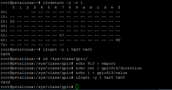
This subsystem provides 32-bit (4 x 8-bit) of general purpose parallel input and output (I/O) expansion for the I2C bus protocol. Address of this module is 0x20. This module contains four 8-bit registers for reading (GPIO_input[7:0] to GPIO_iput[31:24]) and four registers for writing (GPIO_output[7:0] to GPIO_output[31:24]) separately with 0x00 to 0x03 address. These registers can be accessed with I2C commands in linux console or with i2c functions in FSBL code. To access these registers the following commands in linux console can be used:
To see the i2c bus addresses : i2cdetect -y -r 1
To read register of i2c to GPIO module: i2cget -y 1 0x20 <register address>
To write data in a register of i2c to GPIO module: i2cset -y 1 0x20 <register address> <data>
I2C to GPIO
The MIO7 pin is connected to third bit of GPIO input of the I2C to GPIO subsystem (GPIO_input(2)) .To test the I2C to GPIO the MIO7 state can be changed and the value of the first register (register address 0x00) can be monitored. The initial value of this register depends on the CPLD firmware and can be variable. In the following example the initial value of this register is equal to 0x39. That means that initial value of MIO7 is zero. Now set MIO7 to one and read the value of the first register with address 0x00 again. It should be equal to 0x3D. LED1 (Green LED) glows, if MIO7 is set high:
To read the first register of the subsystem:
i2cget -y 1 0x20 0x00 → For example here is equal to 0x39. Here 0x20 is device address and 0x00 is register address.
To set MIO7 to one:
cd /sys/class/gpio/
echo 913 > export
echo out > gpio913/direction
echo 1 > gpio913/value
To read the first register of the subsystem again:
i2cget -y 1 0x20 0x00 → It should be equal to 0x3D.
Example
The subsystem I2C to GPIO port mapping is according the following table:
I2C to GPIO | Pin name | CPLD Pin | Direction | FPGA Pin | Description |
|---|---|---|---|---|---|
sda_in | X7 | M1 | from FPGA | N22 | |
sda_out | X5 | J1 | to FPGA | P22 | If X7 is Low, this pin will be disconnected. |
sclk | X1 | F1 | from FPGA | L16 | |
| SDA | SDA | P7 | To/From RTC and MEMS | -- | I2C data pin of ISL12020MRZ RTC chip / I2C data pin of MEMS chip (LSM303DTR) U22 |
| SCL | SCL | P8 | To RTC and MEMS | -- | I2C clock pin of ISL12020MRZ RTC chip / I2C clock pin of MEMS chip (LSM303DTR) U22 |
GPIO_input | Mapping the GPIO_input bits to various ports or signals | ||||
GPIO_output | Not used | ||||
GPIO input bit mapping:
GPIO_input bit | Connected to: |
|---|---|
0 | PHY_LED0 |
1 | PHY_LED1 |
2 | MIO7 |
3 | NOSEQ |
4 | RESIN_g |
5 | EN1_g |
6 | BOOTMODE_LATCHED |
7 | BOOTMODE_IN |
8 | INT1 |
9 | INT2 |
10 | RTC_INT |
11 | PHY_LED2 |
12 | '0' |
13 | '0' |
UNI/O MAC read block
UNI/O bus is a low speed serial interface for embedded systems that requires only one logic signal SCIO (Serial Clock, Data Input/Output). By using Manchester encoding techniques, the clock and data are combined into a single, serial bit stream (SCIO),where the clock signal is extracted by the receiver to correctly decode the timing and value of each bit. The serial EEPROM (U17) interface is UNI/O. The UNI/O bus uses a master/slave configuration. In this system the serial EEPROM chip is slave and a UNI/O subsystem in CPLD works as master. Both master and slave can operate as transmitter or receiver, but the master device determines which mode is active.The UNI/O MAC read block in CPLD reads the MAC address from serial EEPROM chip during power-on.
UNI/O
uio_sm_cnt[8:5] | uio_io_data |
|---|---|
0000 | MIO7 |
0001 | RTC_INT |
0010 | INT1 |
0100 | INT2 |
0011 | PHY_LED0 |
0100 | PHY_LED1 |
0101 | PHY_LED2 |
0110 | BOOTMODE_IN |
0111 | MIO14 |
1000 | MIO15 |
1001 | XIO4 |
1010 | XIO5 |
1011 | XIO6 |
1100 | WD_HIT |
1101 | '0' |
1110 | '0' |
Multiplexing uio data output between uio-id and uio-io:
uio_sm_cnt[2:1] | uio_sm_cnt(4) | uio_unidir |
|---|---|---|
01 | - | '0' |
10 | '0' | uio_id_data |
10 | '1' | uio_io_data |
SC Pins to B2B
Name | B2B | Mode | Default function | Alternative | Description |
|---|---|---|---|---|---|
EN1 | JM1-Pin 28 | input, weak pull-up | Power Enable | IO | High enables the DC-DC converters and on-board supplies. Not used if NOSEQ=1 |
MODE | JM1-Pin 32 | input, weak pull-up | Boot mode | SDA or IO | Force low for boot from the SD Card. Latched at power on only, not on soft reset! |
NOSEQ | JM1-Pin 7 | input, weak pull-down | Power sequencing Control | Output | Forces the 1.0V and 1.8V DC-DC converters always ON when high. Can be used as an I/O after boot. |
PGOOD | JM1-Pin 30 | output, open drain | Power good | SCL or IO | Forced low until all on-board power supplies are working properly. Attention: During CPLD programming, this pins is high impedance. |
RESIN | JM2-Pin 18 | input, weak pull-up | Reset input | IO | Active Low Reset input, default mapping forces POR_B reset to Zynq PS |
SC Pins to FPGA
Schematic net name | VHDL Name | Default function | Direction | SC pin | FPGA pin | Description |
|---|---|---|---|---|---|---|
XCLK | XCLK | ETH PHY Clock to FPGA | to FPGA | K1 | K19 | |
X7 | X7 | I2C Data from FPGA | from FPGA | M1 | N22 | SDA from EMIO I2Cx |
X5 | X5 | I2C Data to FPGA | to FPGA | J1 | P22 | SDA to EMIO I2Cx |
X4 | XIO6 | ETH PHY LED2 (PHY_LED2) | to FPGA | D1 | P16 | |
X3 | XIO5 | ETH PHY LED1 (PHY_LED1) | to FPGA | B1 | N15 | RTC, MEMS Interrupt or PHY LED1 |
X2 | XIO4 | ETH PHY LED0 (PHY_LED0) | to FPGA | C2 | M15 | |
X1 | X1 | I2C Clock from FPGA | from FPGA | F1 | L16 | SCL from EMIO I2Cx |
PUDC_B | PUDC_B | Enables internal pull-up resistors on the IOs | to FPGA | E3 | K16 | normally not used tied to fixed level by SC |
NOSEQ Pin
This is a dedicated input that forces the module's 1.0V and 1.8V supplies to be enabled if high. This pin has a weak pull-down on the module. If left open the module will power up in normal power sequencing enabled mode. This pin is 3.3V tolerant. This pin is also connected to the System Management Controller. The SC can read the status of this pin (it can be detected if the module is in power sequencing enabled mode). The SC can also use this pin as output after normal power on sequence.
No Sequencing mode
If the module is powered from a single 3.3V supply and power sequencing is disabled, then NOSEQ pin should be powered from the main 3.3V input. That is VIN, 3.3Vin and NOSEQ should all be tied together to the input 3.3V power rail. Sequencing mode should not be used if VIN is not 3.3V.
Normal mode
For normal operation leave NOSEQ open or pull down with a resistor.
Normal mode with user function on NOSEQ
NOSEQ can be used as an output after boot. NOSEQ must be low when 3.3V power is applied to the module. Common usage is an LED connected between NOSEQ and GND. The mapping of NOSEQ pin can be changed by CR1 register. The CR1 register is control register of MDIO slave interface that its content can be changed with FSBL code, uboot command or in linux console directly.
SC MDIO Interface
Most registers and functions are available via ETH PHY Management interface (MIO pins 52 and 53).
Address
| Addr | R/W | Register name | Description |
|---|---|---|---|
0 | RO | ||
1 | RO | ||
2 | RO | ID1 | PHY Identifier Register 1 |
3 | RO | ID2 | PHY Identifier Register 2 |
4 | RW | --- (register4) | register4 = CR5[15:14] & BOOTMODE_GEN & PUDC & CR5[10:8] & CPLD_REVISION BOOTMODE_GEN, PUDC and CPLD_REVISION are generic parameters. CR5[9:8] = boot mode CR5[10] = CPLD boot mode flag (if active '1' → boot mode adjustment via linux console) CR5[15:14] = WDT status |
5 | RW | CR1 (register5) | Control Register 1: LED's |
6 | RW | CR2 (register6) | Control Register 2; XIO Control |
7 | RW | CR3 (register7) | Control Register 3; Reset, Interrupt |
8 | RO | SR1 (register8) | Status Register |
9 | RO | MAChi (register9) | Highest bytes of primary MAC Address |
0xA | RO | MACmi (register10) | Middle bytes of primary MAC Address |
0xB | RO | MAClo (register11) | Lowest bytes of primary MAC Address |
0xC | RO | CR4 (register12) | reserved do not use |
0xD | RW | MMD_CR (register13) | MMD Control Register |
0xE | RW | MMD_AD (register14) | MMD Address/Data |
0xF | - | --- (register15) | reserved do no use |
other | - | reserved do not use |
Register Overview
To adjust desired boot mode in linux console or in FSBL code are used registers CR3(register7), CR4(register12) , CR5 and register4. These registers are used for communication between user, CPLD and FPGA. The format of these registers is shown in the following tables:
| Register | Bit 15...8 | Bit 7...0 | Description |
|---|---|---|---|
CR3 (register7) | Software WDT and Hardware WDT activation /External reset enable 0xA5 → Software WDT active | connected to some signals/ports that is shown in the related following table. | CR3 register is register7 in mdio slave interface. CR3 can be written by user: |
| Register | Bit 15...12 | Bit 11...10 | Bit 9...8 | Bit 7...0 | Description |
|---|---|---|---|---|---|
CR4 (register12) | Control bits for boot modes 1001 → Soft boot mode active | Reserved | boot mode 00 → Undefined | Software WDT time value | CR4[9:8] bits are written by user to define desired boot mode in linux console or in FSBL code. CR4[15:12] bits is used by user to reset FPGA after defining boot mode. CR4 register is register12 in mdio slave interface. CR4 can be written by user. For example: |
| Register | Bit 15...14 | Bit 13...12 | Bit 11 | Bit 10 | Bit 9...8 | Bit 7...0 | Description |
|---|---|---|---|---|---|---|---|
register4 | Watchdog timer status 00 → WDT deactivated | Boot mode generic parameter 00 → QSPI/SD Card | PUDC generic parameter 0 → Pull-up | Software boot mode adjustment active 0 → CPLD boot mode deactivated | Boot mode 00 → Undefined | CPLD_REVISION generic parameter | User does not have access to this register. |
Register CR1
CR1 | related function |
|---|---|
15 | Enable Extra_Enable |
14 | WD_HIT generation |
13 | Undefined |
12 | Undefined |
11:8 | NOSEQ Mux |
7:4 | LED1 Mux |
3:0 | LED2 Mux |
Register CR2
CR2 | related function |
|---|---|
15:12 | XCLK Mux |
11:8 | XIO6 Mux |
7:4 | XIO5 Mux |
3:0 | XIO4 Mux |
Register CR3
CR3 | related port/signal |
|---|---|
0 | INT1 |
1 | INT2 |
2 | RTC_INT |
3 | PHY_LED2 |
4 | OTG_RST |
5 | ETH_RST |
6 | MMC_RST |
7 | EN_ETH_CLK |
15:8 | WDT enable/ Extra enable |
Register CR4
CR4 | related function |
|---|---|
7:0 | WDT time |
| 9:8 | Boot mode |
| 11:10 | Undefined |
| 15:12 | Control bit for boot mode |
Register SR1
SR1 | related function |
|---|---|
0 | INT1 |
1 | INT2 |
2 | RTC_INT |
3 | PHY_LED2 |
7 | BOOTMODE_LATCHED |
8 | BOOTMODE_IN2 |
9 | BOOTMODE_IN |
10 | NOSEQ |
11 | NOSEQ_LATCHED |
12 | WD_EVENT |
13 | PG_1V5 |
14 | EXTRA_ENABLED or WDOG_ENABLED |
15 | mac_valid |
Register Details
Register CR1
The mapping of LED1(Green) , LED2(Red) and NOSEQ pin depends on the value of CR1 register.
CR1[3:0] | LED1 (Green) D2 | CPLD | Description |
|---|---|---|---|
0001 | PHY_LED0 | Input/Output | LED output 0 of Ehternet transceiver chip |
0010 | PHY_LED1 | Input/Output | LED output 1 of Ehternet transceiver chip |
0011 | PHY_LED2 | Input/Output | LED output 2 or interrupt output pin (Active Low) of Ehternet transceiver chip |
0100 | MIO7 | Input | GPIO |
0101 | RTC_INT | Input | Interrupt output or frequency output of RTC chip |
0110 | OFF | ||
0111 | ON | ||
1000 | XIO4 | Input/Output | CPLD pin to the FPGA (M15). ETH PHY LED0 |
1001 | Not MIO14 | Input/Output | |
1010 | Not MIO14/Not MIO15 | Input/Output | |
others | MIO7 | Input | Default value for CR1[3:0] is 0000. GPIO |
CR1[7:4] | LED2 (Red) D5 | CPLD | Description |
0001 | PHY_LED0 | Input/Output | LED output 0 of Ehternet transceiver chip |
0010 | PHY_LED1 | Input/Output | LED output 1 of Ehternet transceiver chip |
0011 | PHY_LED2 | Input/Output | LED output 2 or interrupt output pin (Active Low) of Ehternet transceiver chip |
0100 | MIO7 | Input | GPIO |
0101 | RTC_INT | Input | Interrupt output or frequency output of RTC chip |
0110 | OFF | ||
0111 | ON | ||
1000 | XIO5 | Input/Output | CPLD pin to the FPGA (N15). ETH PHY LED1 |
1001 | Not MIO15 | Input/Output | |
1010 | Not MIO14/Not MIO15 | Input/Output | |
others | modeblink | Signal | If SD card boot mode is selected on the carrier board (for examle for TE0703 S2-4 DIP switch ON) , LED2 flashs slow otherweise LED2 flashs fast. |
CR1[11:8] | NOSEQ | CPLD | Description |
0001 | PHY_LED0 | Input/Output | LED output 0 of Ehternet transceiver chip |
0010 | PHY_LED1 | Input/Output | LED output 1 of Ehternet transceiver chip |
0011 | PHY_LED2 | Input/Output | LED output 2 or interrupt output pin (Active Low) of Ehternet transceiver chip |
0100 | MIO7 | Input | GPIO |
0101 | RTC_INT | Input | Interrupt output or frequency output of RTC chip |
0110 | OFF | ||
0111 | ON | ||
1000 | XIO6 | Input/Output | CPLD pin to the FPGA (P16). ETH PHY LED2 |
1001 | uio_unidir | Signal | |
1010 | Undefined | ||
others | PHY_LED0 | Input/Output | Default value for CR1[11:8] is 0000. LED output 0 of Ehternet transceiver chip |
| CR1(12) | --- | --- | --- |
| --- | Undefined | --- | --- |
| CR1(13) | --- | --- | --- |
| --- | Undefined | --- | --- |
| CR1(14) | WDT Counter | CPLD | Description |
| 0 | counts | Register | CR1(14) = WD_HIT If WD_HIT = '0' --> If WD_counter = WD_time --> WD_RST = '1' --> WD happens |
| 1 | reset | Register | If WD_HIT = '1' --> WD_RST = '0' --> WD will not happen and the WD_counter will be reset. |
| CR1(15) | Extra Reset | CPLD | Description |
| 0 | Disable | Register | |
| 1 | Enable | Register |
Register CR2
The mapping of CPLD IOs (XIO4,XIO5,XIO6 and XCLK) that are connected directly with FPGA, can be changed using CR2 register.
CR2[3:0] | XIO4 | CPLD | Description |
|---|---|---|---|
0001 | MIO7 | Input | GPIO |
0010 | SHA_IO | Input/Output | SDA for CryptoAuthentication Chip |
0011 | MAC_IO | Input/Output | Serial Clock/Data input/Output of Serial EEPROM |
1000 | uio_unidir | Signal | |
0110 | 'Z' | ||
0111 | Undefined | ||
others | PHY_LED0 | Input/Output | Default value for CR2[3:0] is 0000. |
CR2[7:4] | XIO5 | CPLD | Description |
0001 | MIO14 | Input/Output | RX pin of UART0 (FPGA Zynq PS) |
0010 | Undefined | ||
0011 | RTC_INT | Input | Interrupt output or frequency output of RTC chip |
1000 | uio_unidir | Signal | |
0110 | 'Z' | ||
0111 | Undefined | ||
others | PHY_LED1 | Input/Output | Default value for CR2[7:4] is 0000. |
CR2[11:8] | XIO6 | CPLD | Description |
0001 | MIO15 | Input/Output | TX pin of UART0 (FPGA Zynq PS) |
0010 | Undefined | ||
0011 | osc_clk | Signal | This pin is directly connected to on-chip oscillator signal. (24.18MHZ) |
1000 | uio_unidir | Signal | |
0110 | 'Z' | ||
0111 | INTR | Signal | INTR signal can be depending on CR3 register value connected to one of the following interrupt signals: INT1, INT2, RTC_INT, PHY_LED2 |
others | PHY_LED2 | Input/Output | Default value for CR2[11:8] is 0000. |
CR2[15:12] | XCLK | CPLD | Description |
0001 | RTC_INT | Input | Interrupt output or frequency output of RTC chip |
0010 | osc_clk | Signal | This pin is directly connected to on-chip oscillator signal. (24.18MHZ) |
0011 | Undefined | ||
1000 | Undefined | ||
0110 | Undefined | ||
0111 | Undefined | ||
others | CLK_125MHZ | Input | Default value for CR2[15:12] is 0000. This pin is connected to output clock pin of ethernet transceiver chip. |
Register CR3
CR3 bit | Name | CPLD | Description |
|---|---|---|---|
0 | INT1 | Input | MEMS interrupt 1 |
1 | INT2 | Input | MEMS interrupt 2 |
2 | RTC_INT | Input | Real time clock interrupt |
3 | PHY_LED2 | Input/Output | Interrupt output pin of ethernet transceiver |
4 | OTG_RST | Output | Reset for high speed USB transceiver |
5 | ETH_RST | Output | Reset for ethernet transceiver / Reset for serial for unio mac read core |
6 | MMC_RST | Output | Reset for MMC |
7 | EN_ETH_CLK | Output | Enable for ETH clock |
15:8 | WDT enable/ Extra enable | Register | Enable watchdog timer (0xA5) / Enable Extra enable (0xE5) |
Register CR4
CR4 bits | related function | CPLD | Description |
|---|---|---|---|
7:0 | WDT time | Register | if CR4[7:0]=0x00 → WDT_time=0x07 |
| 9:8 | Boot mode | Register | boot mode 00 → Undefined |
| 11:10 | Undefined | ---- | ---- |
| 15:12 | Control bits for boot modes | Register | 1001 → Soft boot mode active |
Note that the time of WDT depends on WTD_time register and the CPLD internal oscillator clock frequency. Default value for CR4 is 0x0000.
Register SR1
SR1 | Description |
|---|---|
0 | INT1 |
1 | INT2 |
2 | RTC_INT |
3 | PHY_LED2 |
7 | BOOTMODE_LATCHED |
8 | BOOTMODE_IN2 |
9 | BOOTMODE_IN |
10 | NOSEQ |
11 | NOSEQ_LATCHED |
12 | WD_EVENT |
13 | PG_1V5 |
14 | EXTRA_ENABLED or WDOG_ENABLED |
15 | mac_valid |
On-board LEDs
There are 3 on-board LEDs, with two of them connected to the System Management Controller and one to the Zynq PL (Done pin).
Name | Color | Connected to: | Default mapping: |
|---|---|---|---|
LED1 | Green | SC | PL MIO[7] |
LED2 | Red | SC | Boot Mode Blink (Fast → SPI, Slow→ SD Card) |
LED3 | Green | Zynq PL | FPGA Done - Active Low |
LED Status Codes
# | LED1 Green | LED2 Red | LED3 Green | Status | Description |
|---|---|---|---|---|---|
1 | OFF | OFF | ON | Fatal power error | This combination after power up is only possible in no sequencing compatibility mode were 3.3Vout is supplied externally. The 1.0V and 1.8V DC-DC supplies are forced on (NOSEQ=1), and the SC is not able to start (3.3Vin below 2.1V). This should never happen if the external power supplies are OK. |
2 | OFF | ON | OFF | VIN missing (or EN1 low) | 3.3Vin is present, but the DC-DC supplies are not powered or 3.3Vin is below 3.05V. If the LEDs stay on in this state then 3.3Vout is not turned on, and the Zynq is kept in the POR state. |
3 | OFF | 1/2 Blink Fast 4 Hz | ON | OK | Boot mode selected is SPI Flash. This status remains after boot also if the LED settings are not changed and user is not controlling MIO7 and FPGA is not loaded. |
4 | OFF | 1/2 Blink Slow 1 Hz | ON | OK | Boot mode selected is SD Card. This status remains after boot also if the LED settings are not changed and user is not controlling MIO7 and FPGA is not loaded. |
5 | MIO7 or user function | Blink or user function | OFF | OK | LED3 goes off when the FPGA is configured. NOTE: The FPGA design can control this LED too using STARTUPE2, so it may remain ON or be flashing when the FPGA is configured. |
6 | ON | Slow blink 0.5Hz, 1/8 on, 7/8 off | OFF | Powerdown | EN1 input to the module is low. If sequencing is enabled in this mode, then all power supplies on the module are OFF. |
7 | ON | Slow blink 0.5Hz, 1/8 on, 7/8 off | ON | EN1 input to the module is low. Sequencing is disabled module is in reset state. | |
8 | ON | ON | ON | Reset | Powered, RESIN input is active low or Bank B34 Supply Voltage is missing. |
LED1 Green
This LED is mapped to MIO7 after power up. After the Zynq PS has booted it can change the mapping of this LED. If SC can not enable power to the Zynq then this LED will remain under SC control. It is available to the user only after the power supplies have stabilized and the POR reset to the Zynq is released. If softwarte watch dog timer is activated this LED will be assigned to the 7th bit of the counter of watch dog timer. By activating hardware WDT this LED will assign input clock of FPGA (Pin K20- CPLD pin X6).
LED1(Green) | Condition | Description |
|---|---|---|
WD_counter(7) | Software WDT activated / Hardware WDT on a board without WDT chip activated | If software WDT is activated, green LED will blink with frequency about 1 HZ. |
ON | POR_B_i = '0' | POR_B_i is '0' if one of the following signals is '0' ---> EN1 or RESIN or PG_ALL or PORDONE |
| X6 | Hardware WDT is activated and WDT chip exists on the board. | X6 is forwarded clock that is generated by FPGA. This signal can be monitored with oscilloscope. The frequency of this signal can be at least 32 HZ. |
Variable | else | Mapping depends on the CR1[3:0] value |
LED2 Red
This LED is used to show various signal or port states. The function of this LED can be changed by CR1 register.
LED2(Red) | Condition | Description |
|---|---|---|
powerblink | EN1_g = '0' | EN1_g is delayed EN1. |
ON | POR_B_i = '0' | |
Variable | else | Mapping depending on the CR1[7:4] value |
LED3 Green (FPGA Done)
This green LED is connected to the FPGA Done pin which has an active low state. As soon as the Zynq is powered and the 3.3V I/O voltage is enabled, this LED will illuminate. This indicates that the Zynq PL is not configured. Once the Zynq PL has been configured the LED will go off.
During normal operation when the Zynq PL has been configured, the LED can be controlled from the FPGA fabric. Control of the LED in a user design requires the use of Xilinx startup primitive rather than a normal I/O primitive. If the startup primitive is not used then the LED will go off after configuration and remain off irrespectively of the user design.
This LED can not be controlled by the SC. If green LED3 does not light up at least for short time at power then there is major problem with power supplies, FPGA core and aux voltages may be missing.
CR registers access methods
System Controller can be accessed as PHY with address 0x1A on the ETH0 Management bus (MIO pins 52, 53). PHY at address 0x00 is the ETH0 onboard ethernet PHY Marvell 88E1512. PHY at address 0x1A is the System Controller. OUI 0x7201 should be decoded as Model TE0720-01. Model 0x01 is Assembly option. Rev 0x00 is the firmware major revision for the System Controller (Rev 0 is the initial version). The CR registers have individual number to be accessed in FSBL code or Linux console. These numbers are defined in mdio_slave_interface subsystem in CPLD VHDL code. Refer to SC registers to see the table of CR registers.
The CR registers can be accessed in three methods. It can be used u-boot functions , FSBL code or phytool command in linux console to access these registers.
MDIO
FSBL code
It is possible to access the CR registers in FSBL code. The following functions are used to write or read these resgisters.
LONG XEmacPs_PhyWrite(XEmacPs *InstancePtr, u32 PhyAddress, u32 RegisterNum, u16 PhyData) → To write in CR registers
LONG XEmacPs_PhyRead(XEmacPs *InstancePtr, u32 PhyAddress, u32 RegisterNum, u16 *PhyDataPtr) → To read CR registers
Note that to access this registers in FSBL code it must be written the following instruction before above commands:
Mac_Config = XEmacPs_LookupConfig(XPAR_PS7_ETHERNET_0_DEVICE_ID); if(Mac_Config == NULL) { return XST_FAILURE; }Status = XEmacPs_CfgInitialize(&Emac, Mac_Config, Mac_Config->BaseAddress); if(Status != XST_SUCCESS){ return XST_FAILURE; }
For example to write 0x0077 in CR1 register the following instruction is used:
XEmacPs_PhyWrite(&Emac, 0x1A, 5, 0x0077);
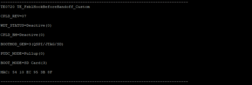
Note that the CR register names are CR1, CR2 , CR3 and CR4. But these registers are named in FSBL code register5, register6, register7 and register12 subsequently. CPLD revision,Boot mode,watchdog timer status and other features of the board will be shown by FSBL code while booting.The format of these information are shown in the following:
| WDT STATUS | Software Adjusted Boot Mode | Hardware Adjusted BOOT MODE | PUDC Mode | Current Boot Mode | CPLD REVISION | Description |
|---|---|---|---|---|---|---|
| Deactive | Deactive | QSPI/SD | Pull down | JTAG | ||
| Hardware_WDT | Active | QSPI/JTAG | Pull up | QSPI | ||
| Software_WDT | ---- | JTAG/SD | ---- | SD Card | ||
| No WDT on the board. Software_WDT with PL clock | ---- | default QSPI/JTAG/SD | ---- | ---- |
U-boot
Communication between Zynq and CPLD chip in mdio bus can be established anytime when ETH0 and management interface are enabled also before FPGA PL Fabric is configured too.
To write a value into CR registers or to read one of them the following instructions can be used:
mii read <addr> <reg>
mii write <addr> <reg> <data>
Module identification code can be read with the following u-boot command in u-boot :
zynq-uboot> mii read 0x1a 0x02 → For TE0720 = 0x01C8
For example to read CR4 register the following instruction can be written in U-Boot command console:
zynq-uboot> mii read 0x1A 0x0C
For example to write 0x0077 in CR1 can be written:
zynq-uboot> mii write 0x1A 5 0x0077
LED1 and LED2 will be switched on.
Linux
It is possible to write into CR registers and to read these registers in Linux console directly. To access the CR registers it must be added ethtool package , while linux image file is generated. To activate this option in petalinux this package must be chosen in configuration of rootfs in petalinux. The path for this package is: Filesystem packages/console/network/ethtool
If this package is installed , phytool command can be used to access the CR registers. Phytool command format is:
phytool read device/addr/register
phytool write device/addr/register <value>
For example to switch on LED1 and LED2 it must be written 0x0077 value in the register CR1:
phytool eth0/0x1A/5 0x0077
To switch off these LEDs execute this instruction:
phytool eth0/0x1A/5 0x0066
Reading MAC address
It can be read MAC-address automatically. Customized u-boot reads MAC address and stores it in environment variables as required. Setting up MAC Address for Linux involves dynamic rewrite of FDT, this is done with u-boot script that starts Linux.
To read MAC address automatically, the following steps must be implemented:
In the FSBL code it must be written the following code additionally. This c file can be found in the following path: \test_board\sw_lib\sw_apps\zynq_fsbl\src\te_fsbl_hooks_te0720.c
For more information refer to TE0720 test board
te_fsbl_hooks_te0720.c
u32 TE_FsblHookBeforeHandoff_Custom(void)
{
...
Mac_Config = XEmacPs_LookupConfig(XPAR_PS7_ETHERNET_0_DEVICE_ID); if(Mac_Config == NULL) { return XST_FAILURE; }
Status = XEmacPs_CfgInitialize(&Emac, Mac_Config, Mac_Config->BaseAddress); if(Status != XST_SUCCESS){ return XST_FAILURE; }
/*
* Read out MAC Address bytes
*/
Status = XEmacPs_PhyRead(&Emac, 0x1A, 9, &rval16); if(Status != XST_SUCCESS){ return XST_FAILURE; }
mac_addr[0] = (unsigned char)(rval16 >> 8);
mac_addr[1] = (unsigned char)(rval16 & 0xFF);
Status = XEmacPs_PhyRead(&Emac, 0x1A, 10, &rval16); if(Status != XST_SUCCESS){ return XST_FAILURE; }
mac_addr[2] = (unsigned char)(rval16 >> 8);
mac_addr[3] = (unsigned char)(rval16 & 0xFF);
Status = XEmacPs_PhyRead(&Emac, 0x1A, 11, &rval16); if(Status != XST_SUCCESS){ return XST_FAILURE; }
mac_addr[4] = (unsigned char)(rval16 >> 8);
mac_addr[5] = (unsigned char)(rval16 & 0xFF);
...

/*
* Write MAC Address to OCM memory for u-boot to import!
*
*/

//strcpy(0xFFFFFC04, "ethaddr=00:0a:35:00:00:05\n" );
#ifdef UBOOT_ENV_MAGIC
Xil_Out32(UBOOT_ENV_MAGIC_ADDR, UBOOT_ENV_MAGIC); // Magic!
MacToUbootEnvironment((char*)UBOOT_ENV_ADDR, mac_addr);

/*
* Set MAC Address in PS7 IP Core registers
*/
Status = XEmacPs_SetMacAddress(&Emac, mac_addr, 1); if(Status != XST_SUCCESS){ return XST_FAILURE; }
...
}
Add the following definition in petalinux-configuration platform-top header file:
platform-top.h code example
#define CONFIG_PREBOOT "echo U-BOOT for petalinux;echo importing env from FSBL shared area at 0xFFFFFC00; if itest *0xFFFFFC00 == 0xCAFEBABE; then echo Found valid magic; env import -t 0xFFFFFC04; fi;setenv preboot; echo; dhcp"
The platform-top.h file can be found in the following path: \petalinux\project-spec\meta-user\recipes-bsp\u-boot\files
The Zynq SoC reads the MAC address from EEPROM by CPLD during power-on and copies this data in OCM (On-chip Memory). After that either in Linux or Uboot console MAC address can be accessed.
Appx. A: Change History and Legal Notices
Revision Changes
- changes REV06 to REV07
- Added matched functions for WDT Chip BD39040MUF-CE2
PG_ALL pin pulled up.
User can activate WDT as before.
If no WDT chip on the board, hardware WDT will be switched automatically on software WDT with PL clock input (X6 pin of CPLD and K20 of FPGA).
If no WDT chip on the board, software WDT will work with CR1(14) clock input as before.
If WDT chip on the board, hardware and software WDT work separately with PL input clock (X6 pin) for hardware WDT and CR1(14) as input clock for software WDT.
For software WDT : phytool write eth0/0x1A/7 0xA500
For hardware WDT : phytool write eth0/0x1A/7 0xB600
Using CR5[15:14] to save the WDT status ("00" WDT deactive, "01" Hardware WDT, "10" Software WDT, "11" No WDT chip on the board, software WDT with PL clock input)
Using Register4 of mdio_slave_interface to see WDT status via FSBL code (first test in vivado 20.2 and vivado 21.2) or following instruction in linux: phytool read eth0/0x1A/4
Boot mode configuration via MDIO interface (phytool)
PGOOD pin is used as boot mode selector pin.
NOSEQ pin is used as tristate via i2c interface.
Reseting the FPGA after boot mode configuration
Matched to FSBL code to show all informations while booting in linux console. For example Boot mode, pudc state ...
Monitoring CR4[15:8] and CR5[10] continuously, to implement a state machine for boot mode configuration correctly.
Using CR4[15:12] as control bit to reset FPGA
Using CR4[9:8] as boot mode configuration , if the FPGA is not restarted still via soft reset.
Defining a new input register for mdio_slave_interface (CR5)
Using CR5[9:8] as boot mode configuration, if the FPGA is restarted already via soft reset.
Using CR5[10] to monitor , if the FPGA is restarted already via soft reset.
Using Register4 to read the generic parameters and other parameters via FSBl code or phytool command in linux : Phytool read eth0/0x1A/4
Using i2c_slave.vhd instead of I2C_to_GPIO.v
Changing Firmware Register MDIO_SL_REGISTER_4_CONTENT to CPLD_REVISION register.
- changes REV05 to REV06
Generic options: PUDC and Boot Mode
MIO7 Pullnone
Adding internal en_3v3_int
JTAG C_* high impedance until 3.3VOUT can be high
Boot mode pins are GND or high impedance until en_3v3_int are high
MIO14,15 high impedance until en_3v3_int are high
JTAG time constraint correction
JTAG drive line adjustment
Bugfix I2C to GPIO module (I2C_to_GPIO.v)
- Changed Firmware Identifier to REV06
changes REV04 to REV05:
0.05 watchdog
changes REV03 to REV04:
NA
changes REV02 to REV03:
NA
changes REV01 to REV02:
added deglicht for EN1 and RESIN inputs
added VCORE ON when 3.3 OK signalled
Identify CPLD Firmware with Trenz FSBL for TE0720
Document Change History
To get content of older revision got to "Change History" of this page and select older document revision number.
Date | Document Revision | CPLD Firmware Revision | Supported PCB Revision | Authors | Description |
|---|---|---|---|---|---|
| REV07 | REV04, |
| |||
| 2022-09-21 | v.138 | REV07 | REV04,REV03,REV02 | Mohsen Chamanbaz |
|
| 2022-06-29 | v.137 | REV07 | REV04,REV03,REV02 | Mohsen Chamanbaz |
|
| 2021-08-28 | v136 | REV06 | REV03, REV02 | John Hartfiel |
|
| 2021-02-16 | v134 | REV06 | REV03, REV02 | Mohsen Chamanbaz |
|
| 2021-02-03 | v.132 | REV06 | REV03, REV02 | Mohsen Chamanbaz |
|
| 2021-01-29 | v.130 | REV05 | REV03, REV02 | John Hartfiel |
|
| 2021-01-14 | v.127 | REV05 | REV03, REV02 | Mohsen Chamanbaz |
|
All |
Legal Notices
Data Privacy
Please also note our data protection declaration at https://www.trenz-electronic.de/en/Data-protection-Privacy
Document Warranty
The material contained in this document is provided “as is” and is subject to being changed at any time without notice. Trenz Electronic does not warrant the accuracy and completeness of the materials in this document. Further, to the maximum extent permitted by applicable law, Trenz Electronic disclaims all warranties, either express or implied, with regard to this document and any information contained herein, including but not limited to the implied warranties of merchantability, fitness for a particular purpose or non infringement of intellectual property. Trenz Electronic shall not be liable for errors or for incidental or consequential damages in connection with the furnishing, use, or performance of this document or of any information contained herein.
Limitation of Liability
In no event will Trenz Electronic, its suppliers, or other third parties mentioned in this document be liable for any damages whatsoever (including, without limitation, those resulting from lost profits, lost data or business interruption) arising out of the use, inability to use, or the results of use of this document, any documents linked to this document, or the materials or information contained at any or all such documents. If your use of the materials or information from this document results in the need for servicing, repair or correction of equipment or data, you assume all costs thereof.
Copyright Notice
No part of this manual may be reproduced in any form or by any means (including electronic storage and retrieval or translation into a foreign language) without prior agreement and written consent from Trenz Electronic.
Technology Licenses
The hardware / firmware / software described in this document are furnished under a license and may be used /modified / copied only in accordance with the terms of such license.
Environmental Protection
To confront directly with the responsibility toward the environment, the global community and eventually also oneself. Such a resolution should be integral part not only of everybody's life. Also enterprises shall be conscious of their social responsibility and contribute to the preservation of our common living space. That is why Trenz Electronic invests in the protection of our Environment.
REACH, RoHS and WEEE
REACH
Trenz Electronic is a manufacturer and a distributor of electronic products. It is therefore a so called downstream user in the sense of REACH. The products we supply to you are solely non-chemical products (goods). Moreover and under normal and reasonably foreseeable circumstances of application, the goods supplied to you shall not release any substance. For that, Trenz Electronic is obliged to neither register nor to provide safety data sheet. According to present knowledge and to best of our knowledge, no SVHC (Substances of Very High Concern) on the Candidate List are contained in our products. Furthermore, we will immediately and unsolicited inform our customers in compliance with REACH - Article 33 if any substance present in our goods (above a concentration of 0,1 % weight by weight) will be classified as SVHC by the European Chemicals Agency (ECHA).
RoHS
Trenz Electronic GmbH herewith declares that all its products are developed, manufactured and distributed RoHS compliant.
WEEE
Information for users within the European Union in accordance with Directive 2002/96/EC of the European Parliament and of the Council of 27 January 2003 on waste electrical and electronic equipment (WEEE).
Users of electrical and electronic equipment in private households are required not to dispose of waste electrical and electronic equipment as unsorted municipal waste and to collect such waste electrical and electronic equipment separately. By the 13 August 2005, Member States shall have ensured that systems are set up allowing final holders and distributors to return waste electrical and electronic equipment at least free of charge. Member States shall ensure the availability and accessibility of the necessary collection facilities. Separate collection is the precondition to ensure specific treatment and recycling of waste electrical and electronic equipment and is necessary to achieve the chosen level of protection of human health and the environment in the European Union. Consumers have to actively contribute to the success of such collection and the return of waste electrical and electronic equipment. Presence of hazardous substances in electrical and electronic equipment results in potential effects on the environment and human health. The symbol consisting of the crossed-out wheeled bin indicates separate collection for waste electrical and electronic equipment.
Trenz Electronic is registered under WEEE-Reg.-Nr. DE97922676.
Overview
Content Tools