The Trenz Electronic TE0728 is a SoC module integrating a Xilinx Automotive Zynq-7020, 512 MByte DDR3 SDRAM with 16-Bit width, 16 MByte Flash Memory for configuration and operation, two 100 Megabit Ethernet transceivers, and powerful switch-mode power supplies for all on-board voltages. A large number of configurable I/O's is provided via rugged high-speed stacking strips.
All this in a compact 6 x 6 cm form factor, at the most competitive price.
All parts are at least automotive temperature range up to +105°C. The module operating temperature range depends on customer design and cooling solution. Please contact us for options.
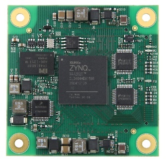 Image Added Image Added
|  Image Added Image Added
|
|---|
PS Peripherals
...
(on-board)
| Chip/Interface | IC | PS7 Peripheral |
|
|---|
| SPI Flash | S25FL127SABMFV10 | QSPI0 | 16 MByte Flash |
| I2C EEPROM | 24xx64 | I2C0 | 8 KByte EEPROM |
| RTC I2C | RV-3029 | I2C0 |
|
| RTC Interrupt | RV-3029 | GPIO - MIO0 |
|
| User LED |
| GPIO - MIO7 |
|
Mapping table for on-board IC to PS7 Peripherals
| MIO Pin | Mapped to | Pull up/down | Notes |
|---|
| 0 | GPIO | Up | RTC Interrupt |
| 1 | QSPI0 |
| |
|
| 4 | QSPI0 | Down | Override to up on base for bootmode change |
| 5 | QSPI0 | Up |
|
|
| 7 | GPIO | Down | On-board LED |
| 8 | CAN1 TXD | Down | CAN transceiver |
in SBC in SBC | SBC SPI Bus | SBC SPI Bus | SBC SPI Bus | | SBC SPI Bus |
|
|
| 14 | I2C0 SCL | Up | On-board RTC, and EEPROM |
| 15 | I2C0 SDA | Up | On-board RTC, and EEPROM |
Recommended Peripheral mapping for MIO Voltage bank 0.
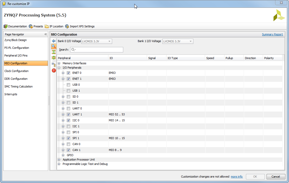 Image Removed
Mapping of on-board peripherals.
PS7 UART
There is no fixed mapping for PS7 UART, if needed it can be mapped to free pins from MIO1 Bank or via EMIO to PL pins.
Recommended mapping for primary (console, debug) UART are MIO52, MIO53 for all cases when MIO1 is not used for off-board Gigabit ETH PHYNote: UART must not be on MIO52,53 different mapping is possible.
PL Peripherals
Both Ethernet PHY IC's are connected to PL pins in Bank 34, all PHY IC pins are connected to FPGA pins, there is no sharing of signals for the two PHY's. PHY's must be operated in MII Mode, other modes are not supported. It is possible to use PS ENET0 or ENET1 via EMIO routing or Ethernet IP Cores implemented in PL Fabric.
.
PUDC pin is connected with pull-up to 3.3V those pre-configuration pull-ups are disabled by default. Strapping resistor exist to change the PUDC mode.
PS and PL Banks
| Bank | VCCIO | B2B I/O Pins | Notes |
|---|
| 500 | 3.3V | 0 |
Vref | MIO1 VREF is connected to resistor divider to support HSTL18 |
| 13 | USER J1.39 B2B | 48 | Differential routing |
| 33 | 3.3V | 33 | Single ended routing |
| 34 | 3.3V | 0 | Ethernet PHY's |
| 35 | 3.3V | 42 | Single ended routing |
| 0 | 3.3V | 4 | JTAG, note 3 pins can be used as input only from PL Fabric |
...
Clock sources
Designator| IC | Description | Frequency | Used as |
|---|
| U14 | MEMS Oscillator | 33. |
3333MHzPS_CLK| 3333 MHz | PS7 PLL clock |
| U5 | MEMS Oscillator |
25MHz| 25 MHz | Ethernet PHY Clock |
| U7 | RTC (internal oscillator) | 32. |
768KHz| 768 KHz | Used by RTC, CLKOUT of RTC not connected |
LED's
| Designator | Color | Connected to | Active Level | IO Standard |
|---|
| D9 | Green | DONE | Low | not applicable |
| D8 | RED | MIO7 | High | not applicable |
| D4 | Green | PL pin V18 | High | LVCMOS33 |
...
XADC Usage
| XADC Pin | Connected to | Notes |
|---|
| VP_0 | SBC MUX_OUT | Resistor divider to adjust ADC Range |
| VN_0 | GND | |
| | | | | XADC is used with internal reference option.
Note the XADC capable pins are not routed differentially to the B2B connector. The performance and usability of the XADC must be evaluated.
SBC
SBC - System Basis Chip MC33908
| SBC Name | Connected | Notes |
|---|
| VDDIO | 3.3V | I/O Voltage fix 3.3V |
| VCCA | J1.17 B2B | Not used on board, external PNP Transistor not used, max 100mA |
| VAUX | - | Not connected, not used |
| SELECT | 5K1 to VPRE | Select 3.3V for VCCA Supply |
| MUX_OUT | XADC | |
| CAN RXD | MIO9 | |
| CAN TXD | MIO8 | |
| LIN RXD | PL Y14 | LIN Soft IP should be implemented in PL Fabric |
| LIN TXD | PL AA14 | |
| MOSI | MIO10 | |
| MISO | MIO11 | |
| SCK | MIO12 | |
| NCS | MIO13 | |
| DEBUG | J1.18 B2B | 11K Pull-down on module, defaults to debug mode DISABLED |
| IO_0 | J1.7 B2B | |
| IO_1 | J1.9 B2B | |
| IO_2 | J1.11 B2B | |
| IO_3 | J1.13 B2B | |
| IO_4 | J1.8 B2B | |
| IO_5 | J1.10 B2B | |
| INTB | J1.12 B2B | If connection to MIO or PL is needed must be implemented on base board |
| FS0B | J1.16 B2B | |
| RSTB | J1.14 B2B | Also forces system Reset |
| CANH | J1.2 B2B | 120R terminator on board, EMI and ESD should be on base board |
| CANL | J1.4 B2B | |
| LIN | J1.20 B2B | Any termination, ESD and EMI circuits should be on base board |
Note: the availability LIN depends on the Module version and assembly option.
Ethernet
There are two 100 MBit Extreme Temperature Ethernet PHY's DP83848YB on the board. Datasheet is available from TI, Literature number SNLS208H. Both PHY's are connected with all I/O Pins to FPGA Bank 34 (VCCIO = 3.3V). PHY Clock 25 MHz source is provided from MEMS Oscillator. All LED outputs have on-board pull-ups. Outputs to Magnetics have also required termination resistors on board.
Both PHY's must be operated in MII Mode, other modes are not supported. It is possible to use PS ENET0 or ENET1 via EMIO routing or Ethernet IP Cores implemented in PL Fabric.
| ETH1 | ETH2 | Pullup | Notes |
|---|
| CTREF | J3.57 | J3.25 |
| Magnetics center tap voltage |
| TD+ | J3.58 | J3.28 | on-board |
|
| TD- | J3.56 | J3.26 | on-board |
|
| RD+ | J3.52 | J3.22 | on-board |
|
| RD- | J3.50 | J3.20 | on-board |
|
| LED1 | J3.55 | J3.23 | on-board |
|
| LED2 | J3.53 | J3.21 | on-board |
|
| LED3 | J3.51 | J3.19 | on-board |
|
| POWERDOWN/INT | L21 | R20 | on-chip | It is recommended to configure FPGA I/O as input with Pullup or as output driving 1 if Interrupt not used. |
| RESET_N | M15 | R16 | on-chip | It is recommended to configure FPGA I/O as input with Pullup or as output (active low PHY Reset). |
It is recommended to add IOB TRUE constraint for the MII Interface pins.
When connecting the PHY's to Zynq PS ETH0, ETH1 EMIO GMII Interfaces it is recommended to use GMII to MII Wrap IP Core. This IP core maps the EMIO GMII to external MII Interface.
Legal Notices
| Include Page |
|---|
| IN:Legal Notices |
|---|
| IN:Legal Notices |
|---|
|
Document Change History
| Date | Revision | Authors | Description |
|---|
| 2015-05-10 | |
| Work in progress |
| All |
...