Page History
| Scroll Ignore |
|---|
Download PDF Version version of this Documentdocument. |
| Scroll pdf ignore | |
|---|---|
Table of Contents
|
Overview
| Scroll Only (inline) |
|---|
Refer to https:// |
...
wiki.trenz-electronic.de/ |
...
display/PD/TE0711+TRM for online version of this manual and the rest of available documentation. |
...
Trenz Electronic TE0711 is an industrial-grade FPGA module integrating a Xilinx Artix-7 FPGA, 32 MByte Quad SPI Flash memory for configuration and operation and powerful switching-mode power supplies for all on-board voltages. Numerous configurable I/O's are provided via rugged high-speed strips. All this on a tiny footprint, smaller than a credit card size at very competitive price. All Trenz Electronic SoM's in 4 x 5 cm form factor follow the same mechanical design rules, thus they are interchangeable.
Block Diagram

Figure 1: TE0711-01 block diagram.
Main Components
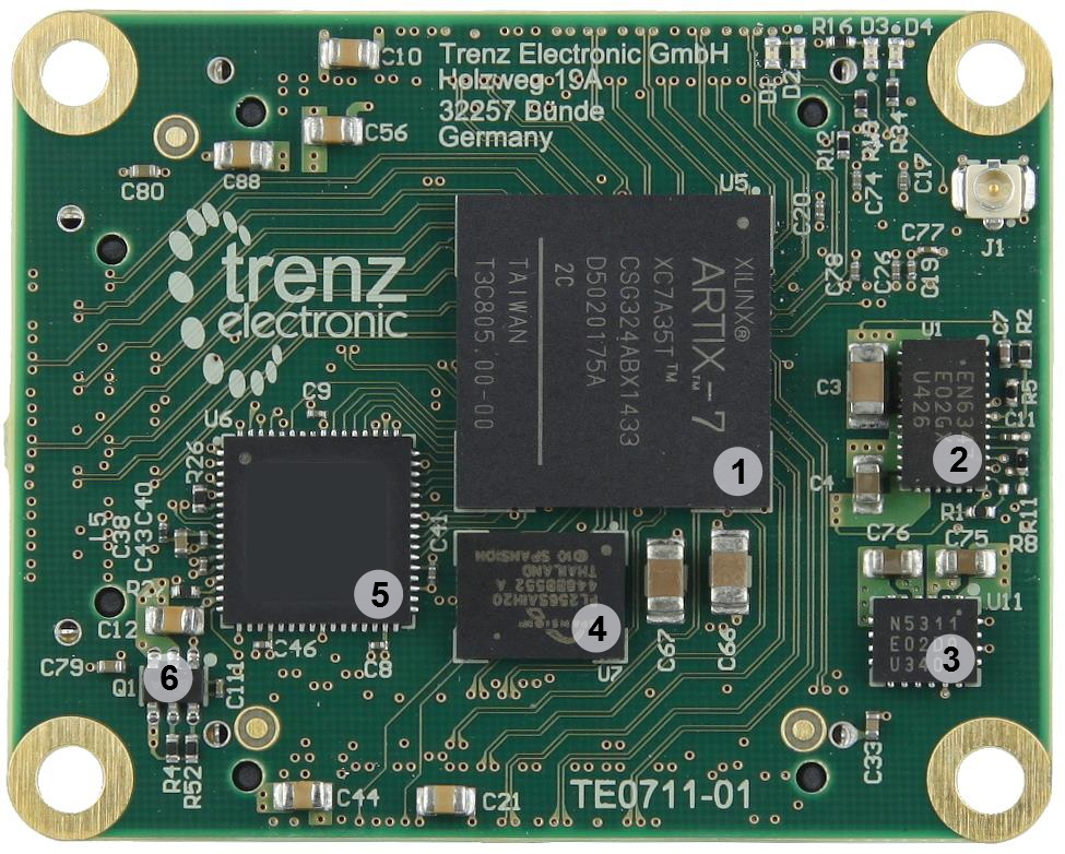
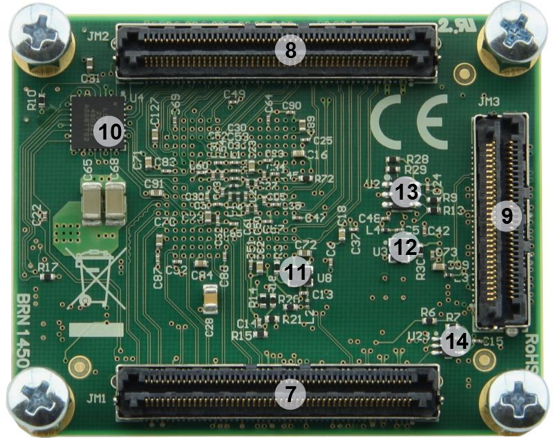
Figure 2: TE0711 (REV 01).
- Artix-7 (15T to 100T) FPGA
- EN6347QI voltage Regulator 1.0V
- EN5311QI voltage Regulator 1.8V
- S25FL256S 32 MByte Quad SPI Flash memory
- Dual USB to UART/FIFO Bridge (FT2232H)
- TPS27082L load switch for 3.3V voltage level
- B2B connector JM1 (0,40 mm Razor Beam™ High Speed Hermaphroditic Terminal/Socket Strip (LSHM-150))
- B2B connector JM2 (0,40 mm Razor Beam™ High Speed Hermaphroditic Terminal/Socket Strip (LSHM-150))
- B2B connector JM3 (0,40 mm Razor Beam™ High Speed Hermaphroditic Terminal/Socket Strip (LSHM-150))
- System Controller CPLD (Lattice LCMXO2-256HC): 256 Macrocell CPLD
- SiT8008AI 100 MHz reference clock (connected to FPGA bank 14)
- SiT8008AI 12 MHz reference clock (connected to USB to UART/FIFO Bridge)
- EEPROM (configuration data for USB to UART/FIFO Bridge)
- TPS3805H33 voltage detector for generating "Power OK"-signal indicating successful power-on-sequencing
Key Features
Industrial-grade Xilinx Artix-7 (15T to 100T) SoM (System on Module), supported by the free Xilinx Vivado WebPACK tool
Rugged for shock and high vibration
- FTDI FT2232HQ USB 2.0 High Speed to UART/FIFO
32 MByte QSPI Flash memory (with XiP support)
100 MHz MEMS oscillator
Plug-on module with 2 × 100-pin and 1 × 60-pin high-speed hermaphroditic strips
178 FPGA I/Os (84 differential pairs) are available on board-to-board connectors
On-board high-efficiency DC-DC converters
4.0 A x 1.0 V power rail
1.0 A x 1.8 V power rail
1.0 A x 1.5 V power rail
System management and power sequencing
eFUSE bit-stream encryption
AES bit-stream encryption
User LED
Evenly-spread supply pins for good signal integrity
Assembly options for cost or performance optimization available upon request.
are mechanically compatible.
Key Features
Industrial-grade Xilinx Artix-7 (15T to 100T) FPGA, supported by the free Xilinx Vivado WebPACK tool
Rugged for shock and high vibration
- FTDI FT2232H USB 2.0 high-speed to UART/FIFO
32 MByte QSPI Flash memory (with XiP support)
100 MHz MEMS oscillator
Plug-on module with 2 × 100-pin and 1 × 60-pin high-speed hermaphroditic strips
178 FPGA I/Os (84 differential pairs) are available on board-to-board connectors
On-board high-efficiency DC-DC converters
4.0 A x 1.0 V power rail
1.0 A x 1.8 V power rail
1.0 A x 1.5 V power rail
System management and power sequencing
eFUSE bit-stream encryption
AES bit-stream encryption
User LED
Evenly-spread supply pins for good signal integrity
Assembly options for cost or performance optimization available upon request.
Block Diagram
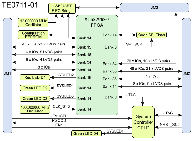
Figure 1: TE0711-01 block diagram.
| Page break |
|---|
Main Components
Figure 2: TE0711-01 PCB.
- Xilinx Artix-7 FPGA, U5
- 4A PowerSoC DC-DC converter for 1.0V (Altera EN6347QI), U1
- 1A PowerSoC DC-DC converter for 1.8V (Altera EN5311QI), U11
- 32 MByte Quad SPI Flash memory 32 MByte Quad SPI Flash memory (Cypress S25FL256S), U7
- Dual USB to UART/FIFO bridge (FTDI FT2232H), U6
- Load switch for 3.3V voltage level (Texas Instruments TPS27082L), Q1
- B2B connector Samtec Razor Beam™ LSHM-150, JM1
- B2B connector Samtec Razor Beam™ LSHM-150, JM2
- B2B connector Samtec Razor Beam™ LSHM-130, JM3
- System Controller CPLD (Lattice Semiconductor LCMXO2-256HC), U4
- 100.000000 MHz reference clock connected to the FPGA bank 14 (SiTime SiT8008), U8
- 12.000000 MHz reference clock connected to the USB to UART/FIFO bridge (SiTime SiT8008), U3
- Configuration data serial EEPROM for USB to UART/FIFO bridge (Microchip 93AA56), U2
- Voltage detector for "Power OK" signalling (Texas Instruments TPS3805H3), U23
Page break
Initial Delivery State
| Storage Component | Content | Notes |
|---|---|---|
SPI Flash OTP Area | Empty, not programmed | Except serial number programmed by flash vendor. |
SPI Flash Quad Enable bit | Programmed | - |
SPI Flash main array | Demo design | - |
EFUSE USER | Not programmed | - |
EFUSE Security | Not programmed | - |
Table 1: Initial TE0711-01 initial delivery state.
Signals, Interfaces and Pins
...
I/O signals connected to the FPGA's I/O banks and B2B connector:
| Bank | Type | B2B Connector | I/O Signal Count |
|---|
0
HR
-
-
| Voltage | Notes | ||
|---|---|---|---|
14 | HR | JM1 JM2 | 8 I/O pins 18 I/O pins, |
(9 LVDS pairs |
) | 3.3V | HR banks support voltages from 1.2V to 3.3V. See Xilinx Artix-7 datasheet (DS181) for voltage ranges. | |
15 | HR | JM1 | 48 I/O pins 24 LVDS pairs |
User | As above. | ||
16 | HR | JM1 | 6 I/O pins 3 LVDS pairs |
1.8V | As above. | ||
| 34 | HR | JM1 JM3 | 48 I/O pins 24 LVDS pairs |
| User | As above. | ||
| 35 | HR | JM2 | 50 I/O pins 24 LVDS pairs |
| User | As above. |
Table 2: Voltage ranges and pin-outs of available logic banks of the FPGA.
Please use Refer to Master Pin-out Table as primary reference for the pin mapping information.
...
| JTAG Signal | B2B Connector |
|---|---|
| TCK | JM2-99 |
| TDI | JM2-95 |
| TDO | JM2-97 |
| TMS | JM2-93 |
Table 3: Pin - mapping of JTAG Interface on B2B connector
...
Special purpose pins are connected to smaller System Controller CPLD and have following default configuration:
| Pin Name | Mode | Function | Default Configuration | B2B Connector |
|---|---|---|---|---|
| STAT_SC2 | Output | Power Good | Active high when all on-module power supplies are working properly. | JM1-30 |
| NRST_SC0 | Input | Reset | Active low reset signal, drive low to keep the system in reset (FPGA pin PROG_B will be driven by CPLD). | JM2-18 |
| JTAGSEL | Input | JTAG Select | Low for normal operation, high (3.3V) to |
| program the System Controller CPLD. | JM1-89 | |||
| EN_SC3 | Input | Enable FPGA Core Voltage supply | High (3.3V) or open for normal operation, low to stop power-on sequencing. | JM1-28 |
Table 4: Pin - description of System Controller CPLD.
LEDs
On the SoM TE0710 there is a total of 3 LEDS available. Two LEDs are status LEDs, one can freely used in costumer designs. The user LED is routed to the FPGA by the net with the schematic-name 'USERLED'.
On-board LEDs
The TE0711 SoM has total of 4 on-board LED's. LED's D1, D2 and D3 are connected to the Xilinx Artix-7 FPGA and can be freely used by user design. LED D4 is the System Controller CPLD status LEDWhen the FPGA is not configured the status LEDs will flash continuously. Finally once FPGA configuration has completed the status LEDs can be used in the user's FPGA design.
| LED | Color | Connected to pin | Description and Notes |
|---|---|---|---|
| D1 | redRed | SYSLED2 | User LED, active HIGH, connected to FPGA Pin A8 |
| D2 | greenGreen | SYSLED4 | User LED, active HIGH, connected to FPGA Pin R17 |
| D3 | green | SYSLED3 | User LED, active LOW, connected to FPGA Pin L15 |
| D4 | green | SYSLED1 | System Controller status LED, connected to CPLD |
Table 5: Description of the on board LEDs
Clocking
The TE0710 is equipped with two MEMS oscillators to provide clock signals for two on-board Ethernet PHY's and DDR3 SDRAM.
...
Reference oscillator clock for USB to UART/FIFO Bridge (FT2232H)
...
12 MHz
...
| User LED, active HIGH, connected to FPGA Pin R17 | |||
| D3 | Green | SYSLED3 | User LED, active LOW, connected to FPGA Pin L15 |
| D4 | Green | SYSLED1 | System Controller status LED, connected to CPLD |
Table 5: Description of on-board LED's.
Clocking
The TE0711-01 is equipped with MEMS oscillator (
...
SiT8008AI-73-XXS-100.000000E
...
, U8) to provide 100 MHz clock signal for Xilinx Artix-7 FPGA pin P17.
On-board Peripherals
32 MByte Quad SPI Flash Memory
On-board
Table 6: Clocks overview
Onboard Peripherals
32 Mbyte Quad SPI Flash Memory
An SPI flash memory S25FL256S (U7) is provided for used to store initial FPGA configuration file storage. After Besides FPGA configuration completes the , remaining free flash memory can be used for user application data storage. All four SPI data lines are connected to the FPGA allowing x1, x2 or x4 data bus widths to be used. The maximum Maximum data rate will be dependent depends on the bus width and clock frequency used.
| Note |
|---|
SPI Flash QE (Quad Enable) bit must be set , to high or the FPGA would not configure from Flash. This bit is always set at manufacturingFPGA is unable to load its configuration from flash. By default this bit is set to high at the manufacturing plant. |
System Controller CPLD
The system controller is used to coordinate the configuration of the FPGA. The FPGA is held in reset (by driving the PROG_B signal) until the power supplies have sequenced. Low level at NRST_SC0 pin also resets the FPGA. This signal can be driven from the user’s PCB via the B2B connector pin JM2-18. Input EN_SC3 is also gated to FPGA Reset and should be open or pulled up for normal operation. EN_SC3 low turns off on board DC-DC converters and stops power-on sequencing.
...
The TE0711-01 SoM has on-board high-speed USB 2.0 High Speed to UART/FIFO IC FT2232HQ FT2232H controller from FTDI. Channel A can only be used in simple UART mode, . Channel B can be used as UART , in FT245 FIFO mode, JTAG (MPSSE) or High Speed Serial mode or in high-speed serial modes.
All FT2232HQ-pins are FT2232H controller is connected to the FPGA bank 14 with fixed 3.3V VCCIO and should be used with LVCMOS33 all signalling must meet the LVCMOS 3.3V I/O Standardstandard.
There is also a standard 256 Byte EEPROM is connected to the FT2232HQFT2232H-chip available to store custom configuration settings. EEPROM These settings can be changed using FTDI provided tools that can be downloaded from FTDI website. See FTDI website for more information.
Power and Power-On Sequence
...
| Power Input Pin | Voltage Range | Max Current |
|---|---|---|
| VIN | 3.3V to 5.5V | Typical 200mA, depending on customer design and connections. |
| 3.3VIN | 3.3V | Typical 50mA, depending on customer design and connections. |
Table 76: maximal current of power suppliesTypical power consumption.
| Tip |
|---|
Vin VIN and Vin 3VIN3.3V can be connected to the same power source (3.3 V3V). |
Lowest power consumption is achieved when powering the module from single 3.3V supply. When using split 3.3V/5V supplies the power consumption (and heat dissipation) will rise, this is due to the DC/DC converter efficiency (it decreases when VIN/VOUT ratio rises).
...
For highest efficiency of on board DC/-DC regulators, it is recommended to use same 3.3V power source for both VIN and 3.3VIN power rails. Although VIN and 3.3VIN can be powered up in any order, it is recommended to power them up simultaneously.
It is important that all baseboard I/O's are 3-stated at power-on until System Controller sets STAT_SC2 signal high (B2B connector JM1, pin 30), or 3.3V is present on B2B connector JM2 pins 10,12 or 91, meaning that all on-module voltages have become stable and module is properly powered up.
See Xilinx Artix-7 datasheet DS181 ( for Artix7) for additional information. User should also Also check related baseboard documentation when choosing baseboard design for TE0711-01 module.
A 3.3V supply is also needed and must be supplied from the user's PCB. An output 3.3V supply is available on some of the board connector pins (see section 'Power Rails'). The input 3.3VIN will be switched to the internal 3.3V voltage level after the FPGA 1.0V supply is stablehas stabilized. Than 3.3V supply will be available on the B2B connector pins.
...
Voltages on B2B- Connectors | B2B JM1-Pin | B2B JM2-Pin | Direction | Note | ||
|---|---|---|---|---|---|---|
| VIN | 1, 3, 5 | 2, 4, 6, 8 | input | supply voltage | ||
| 3.3VIN | 13, 15 | - | input | supply voltage | ||
| VCCIO15 | 9, 11 | - | input | high range bank voltage | ||
| VCCIO34 | - | 1, 3 | input | high range bank voltage | ||
| VCCIO35 | 7, 9 | input | high range bank voltage | |||
| 3.3V | 14 | .3V | - | 10, 12 | output | internal 3.3V voltage level |
| JTAG VREF | - | 10, 12, 91 | output | internal JTAG reference voltage (3.3V voltage level). | ||
| 1.8V | 39 | - | output | internal 1.8V voltage level |
Table 87: Power rails of SoM on B2B connectors.
Bank Voltages
| Bank | Schematic Name | Voltage | Range |
|---|---|---|---|
| 0 Config | 3.3V | 3.3V | - |
| 14 | 3.3V | 3.3V | - |
| 15 | VCCIO15 | user | HR: 1.2V to 3.3V |
| 16 | 1.8V | 1.8V | - |
| 34 | VCCIO34 | user | HR: 1.2V to 3.3V |
| 35 | VCCIO35 | user | HR: 1.2V to 3.3V |
Table 98: Range of FPGA's bank voltages.
See the Artix7 datasheet DS181 for the allowable voltage range.
Board to Board Connectors
| Include Page | ||||||
|---|---|---|---|---|---|---|
|
Variants Currently In Production
Module Variant | FPGA | FPGA Junction Temperature | Operating Temperature Range | TE0711-01-100-2C | XC7A100T-2CSG324C | 0°C to 85°C | Variant | FPGA | FPGA Junction Temperature | Operating Temperature Range | commercial grade|
|---|---|---|---|---|---|---|---|---|---|---|---|
| TE0711-01-35- | 2C2I | XC7A35T- | 2CSG324C2CSG324I | 0°C -40°C to 85°C100°C | commercial Industrial grade | ||||||
| TE0711-01-100-2I | XC7A100T-2CSG324I | -40°C to 100°C | industrial Industrial grade | ||||||||
| TE0711-01-35- | 2I2C | XC7A35T- | 2CSG324I2CSG324C | 0°C to 85°C | Commercial grade | ||||||
| TE0711-01-100-2C | XC7A100T-2CSG324C | 0°C to 85°C | Commercial | -40°C to 100°C | industrial grade |
Table 109: Differences between variants of Module TE0711-01 module variants.
Technical Specifications
Absolute Maximum Ratings
| Parameter | Min | Max | Units | Notes |
|---|---|---|---|---|
VIN supply voltage | -0.3 | 7.0 | V | EN6347QI |
| , EN5311QI |
| datasheet | ||||
| 3.3VIN supply voltage | -0.1 | 3.6 | V | - |
| HR I/O |
| banks supply voltage (VCCO) | -0.5 | 3.6 | V |
| Xilinx datasheet DS181 | |
| HR I/O banks input voltage | -0.4 |
| VCCO |
| + 0.55 | V |
| Xilinx datasheet DS181 |
| Voltage on module JTAG pins | -0.5 |
| VCCO_0 + 0.45 | V | VCCO_0 is 3.3V nominal |
| Storage temperature | -55 | +125 | °C | - |
Table 1110: Absolute maximum ratings.
Recommended
...
Operating Conditions
| Parameter | Min | Max | Units | Notes |
|---|
| VIN supply voltage | 2.4 | 5.5 | V |
| EN5311QI data sheet |
| 3.3VIN supply voltage | 3.135 | 3.465 | V |
3,3V ± 5% |
| HR I/O |
| banks supply voltage |
| (VCCO) | 1.14 | 3.465 | V |
Xilinx datasheet DS181 |
| HR I/O banks input voltage |
| -0.20 | VCCO + 0.2 | V |
Xilinx datasheet DS181 |
| Voltage on |
| JTAG pins | 3.135 | 3.465 | V |
| 3,3V ± 5% |
Table 1211: Recommended operation conditions
...
operating conditions.
Operating Temperature Ranges
...
Industrial grade: -40°C to +85°C.
The module Module operating temperature range depends also on customer design and cooling solution. Please contact us for options.
| Note |
|---|
| Please check Xilinx datasheet (DS181) for complete list of absolute maximum and recommended operating ratings. |
| Page break |
|---|
Physical Dimensions
- Module size: 50 mm × 40 mm. Please download the assembly diagram for exact numbers.
- Mating height with standard connectors: 8mm
- PCB thickness: 1.6mm
- Highest part on PCB: approx. 2.5mm. Please download the step model for exact numbers.
All dimensions are shown in mmmillimeters.


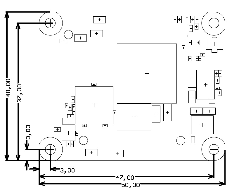
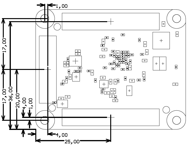
Figure 3: Physical Dimensions dimensions of the TE0711-01 board.
Weight
20.6 g
...
Plain module.
8.8 g
...
Set of nuts and bolts
...
.
Revision History
Hardware Revision History
| Date | Revision | Notes | PCN | Documentation |
|---|
| Link | ||
|---|---|---|
| 2015-01-02 | 01 | First production release |
Current Hardware Revision
| TE0711-01 |
Table 12: Hardware revisions.
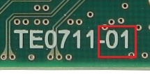
Hardware revision number is printed on the PCB board together with the module model number separated by the dash.
Document Change History
separated by the dash.
Document Change History
| Date | Revision | Contributors | Description | ||||||||
|---|---|---|---|---|---|---|---|---|---|---|---|
| John Hartfiel |
| |||||||||
| 2017-11-10 | v.33 | John Hartfiel |
| ||||||||
| 2017-01-29 | v.30 | Jan Kumann |
|
| 2017-01-01 | v.10 | Ali Naseri, Thorsten Trenz, Jan Kumann |
|
| 2015-06-05 |
| v.1 |
Antti Lukats |
|
Disclaimer
| Include Page | ||||
|---|---|---|---|---|
|
Overview
Content Tools