...
| Page properties |
|---|
|
Template Revision 2.12
- Module: TRM Name always "TE Series Name" +TRM
Example: "TE0728 TRM"
- Carrier: TRM Name usually "TEB Series Name" +TRM
Example: "TEB0728 TRM"
|
| HTML |
|---|
<!-- tables have all same width (web max 1200px and pdf full page(640px), flexible width or fix width on menu for single column can be used as before) -->
<style>
.wrapped{
width: 100% !important;
max-width: 1200px !important;
}
</style>Template Change history: | Date | Version | Changes | Author |
|---|
| 4.2 | | ED |
| 4.1 | | ED |
| 4.0 | - Rework for smaller TRM which can be generated faster
- Reduce Signal Interfaces Pin
- Reduce On Board Periphery
- Reduce Power
- Move Configuration Signals from Overview to own section
| JH |
| 3.12 | - Version History
- changed from list to table
- all
- changed title-alignment for tables from left to center
| ma |
| 3.11 | - update "Recommended Operating Conditions" section
|
|
| 3.1 | - New general notes for temperature range to "Recommended Operating Conditions"
|
|
| 3.02 | - add again fix table of content with workaround to use it for pdf and wiki
- Export Link for key features examples
- Notes for different Types (with and without Main FPGA)
- Export Link for Signals, Interfaces and Pins examples
- Notes for different Types (Modul, Modul Hybrid, Evalboard, Carrier)
|
|
| 3.01 | - remove fix table of content and page layout ( split page layout make trouble with pdf export)
- changed and add note to signal and interfaces, to on board periphery section
- ...(not finished)
|
|
| 3.00 | - → separation of Carrier/Module and evaluation kit TRM
|
|
| 2.15 | - add excerpt macro to key features
|
|
| 2.14 | - add fix table of content
- add table size as macro
|
|
|
| Page properties |
|---|
|
Important General Note:
|
| Page properties |
|---|
|
----------------------------------------------------------------------- |
| Page properties |
|---|
|
Note for Download Link of the Scroll ignore macro: |
Overview
Trenz Electronic TEM0007 module is an industrial-grade FPGA micromodule integrating a Microsemi Polarfire SoC FPGA, Gigabit Ethernet PHY, USB 2.0 PHY, one GByte LPDDR4 SDRAM, 64 MByte SPI Flash memory for configuration and operation, and power supply. A large number of configurable I/Os is provided via robust board-to-board (B2B) connectors.
Refer to http://trenz.org/tem0007-info for the current online version of this manual and other available documentation.
Key Features
| Page properties |
|---|
|
Note:
'description: Important components and connector or other Features of the module
→ please sort and indicate assembly options → See examples for different types <Series Name> TRM Template section examples#%3CSeriesName%3ETRMTemplatesectionexamples-KeyFeatures |
| Excerpt |
|---|
- SoC/FPGA/Module
- RAM/Storage
- On Board
- Interface
- Power
- Dimension
- Notes
|
- SoC/FPGA
- Industrial-grade Microsemi Polarfire SoC MPFS250T-1FCVG484I
- RAM/Storage
- 1 GByte LPDDR4
- 64 MByte SPI Flash Memory
- On Board
- System Controller CPLD
- MAC address serial EEPROM
- Interface
- 10/100/1000 Mbps Gigabit Ethernet PHY
- Highly Integrated Full-Featured Hi-Speed USB 2.0 ULPI Transceiver
- Trenz 4 x 5 module socket connectors (3x Samtec LSHM series connectors)
- Power
- Dimension
Block Diagram
| Page properties |
|---|
|
add drawIO object in Scroll Ignore section and add reference image in Scroll Only.
| Note |
|---|
Title (not anchor) of all Scroll Title such as DrawIOs and Tables should be changed according to the Module name. Example: TE0812 Block Diagram |
| Note |
|---|
All created DrawIOs should be named according to the Module name: Example: DrawIO of TE0812 Block Diagram should be named TE0812_OV_BD |
|
| Scroll Title |
|---|
| anchor | Figure_OV_BD |
|---|
| title-alignment | center |
|---|
| title | TEM0007 block diagram |
|---|
|
| Scroll Ignore |
|---|
| draw.io Diagram |
|---|
| border | true |
|---|
| |
|---|
| diagramName | Figure_OV_BD |
|---|
| simpleViewer | true |
|---|
| width | |
|---|
| links | auto |
|---|
| tbstyle | top |
|---|
| diagramDisplayName | |
|---|
| lbox | true |
|---|
| diagramWidth | 644 |
|---|
| revision | 14 |
|---|
|
|
| Scroll Only |
|---|
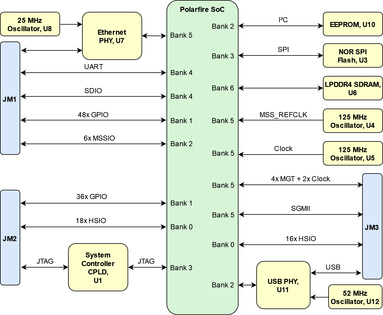 Image Added Image Added
|
|
Main Components
| Page properties |
|---|
|
Notes : - Picture of the PCB (top and bottom side) with labels of important components
- Add List below
Important General Note: If some section is configurable and depends on Firmware, please refer to the addition page (for example CPLD). If not available, add note, that this part is configurableDesignate all graphics and pictures with a number and a description, Use "Scroll Title" macro Use "Scroll Title" macro for pictures and table labels. Figure number must be set manually at the moment (automatically enumeration is planned by scrollPDF)Figure template: | Scroll Title |
|---|
|
| anchor | Figure_anchorname |
|---|
| title | Text |
|---|
|
| Scroll Ignore |
|---|
Create DrawIO object here: Attention if you copy from other page, objects are only linked. |
| Scroll Only |
|---|
image link to the generate DrawIO PNG file of this page. This is a workaround until scroll pdf export bug is fixed |
Table template:
Layout macro can be use for landscape of large tables
| Scroll Title |
|---|
| Table_tablename| Figure_OV_MC | | title-alignment | center |
|---|
| title |
|---|
| Text |
tablelayoutorientationportraitsortDirection | ASC |
| repeatTableHeaders | default |
|---|
style | widths | | sortByColumn | 1 |
|---|
| sortEnabled | false |
|---|
| cellHighlighting | true |
|---|
| Example | Comment |
|---|
| 1 | 2 |
The anchors of the Scroll Title should be named consistant across TRMs. A incomplete list of examples is given below
Use Anchor in the document: add link macro and add "#<anchorname>Refer to Anchror from external : <page url>#<pagename without space characters>-<anchorname>
| Page properties |
|---|
|
----------------------------------------------------------------------- |
| Page properties |
|---|
|
Note for Download Link of the Scroll ignore macro: |
| Scroll pdf ignore |
|---|
Table of Contents |
Overview
Trenz Electronic TEM0007 module is an industrial-grade FPGA micromodule integrating a Microsemi Polarfire SoC FPGA, Gigabit Ethernet PHY, USB 2.0 PHY, one GByte LPDDR4 SDRAM, 64 MByte SPI Flash memory for configuration and operation, and power supply. A large number of configurable I/Os is provided via robust board-to-board (B2B) connectors.
Refer to http://trenz.org/tem0007-info for the current online version of this manual and other available documentation.
...
| |
|---|
| diagramName | TEM0007_OV_MC |
|---|
| simpleViewer | false |
|---|
| width | |
|---|
| links | auto |
|---|
| tbstyle | top |
|---|
| lbox | true |
|---|
| diagramWidth | 641 |
|---|
| revision | 4 |
|---|
|
|
| Scroll Only |
|---|
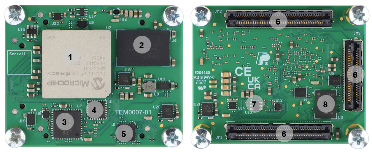 Image Added Image Added
|
|
- Microsemi Polarfire SoC MPFS250T, U2
- 1 GByte LPDDR4 SDRAM, U6
- Integrated 10/100/1000 Mbps Energy Efficient Ethernet Transceiver, U7
- Highly Integrated Full Featured Hi-Speed USB 2.0 ULPI Transceiver, U11
- Lattice Semiconductor MachXO2 System Controller CPLD, U1
- B2B Connector Samtec Razor Beam, JM1...3
- EEPROM, U10
- Serial NOR Flash, U3
Initial Delivery State
| Page properties |
|---|
|
| Note |
|---|
Only components like EEPROM, QSPI flash can be initialized by default at manufacture. If there is no components which might have initial data ( possible on carrier) you must keep the table empty |
|
| Scroll Title |
|---|
| anchor | Table_OV_IDS |
|---|
| title-alignment | center |
|---|
| title | Initial delivery state of programmable devices on the module |
|---|
|
| Scroll Table Layout |
|---|
| orientation | portrait |
|---|
| sortDirection | ASC |
|---|
| repeatTableHeaders | default |
|---|
| style | |
|---|
| widths | |
|---|
| sortByColumn | 1 |
|---|
| sortEnabled | false |
|---|
| cellHighlighting | true |
|---|
|
Storage device name | Content | Notes |
|---|
SPI NOR Flash, U3 | Not programmed |
| | EEPROM, U10 | Pre-programmed globally unique MAC |
| | System Controller CPLD, U1 | Standard firmware |
|
|
Signals, Interfaces and Pins
| Page properties |
|---|
|
For subsection examples see: <Series Name> TRM Template section examples#%3CSeriesName%3ETRMTemplatesectionexamples-Signals,InterfacesandPins | Note |
|---|
- Table with all connectors and Designator
- List of different interfaces per connector
- IO CNT (for FPGA IOs where functionality can be changed by customer)
|
|
Connectors
| Scroll Title |
|---|
| anchor | Table_SIP_C |
|---|
| title-alignment | center |
|---|
| title | Board Connectors |
|---|
|
| Scroll Table Layout |
|---|
| orientation | portrait |
|---|
| sortDirection | ASC |
|---|
| repeatTableHeaders | default |
|---|
| style | |
|---|
| widths | |
|---|
| sortByColumn | 1 |
|---|
| sortEnabled | false |
|---|
| cellHighlighting | true |
|---|
|
| Connector Type | Designator | Interface | IO CNT | Notes |
|---|
|
|
|
|
|
|
|
|
|
|
|
|
|
|
|
|
|
|
|
|
|
|
|
|
|
|
Test Points
| Page properties |
|---|
| Note:
'description: Important components and connector or other Features of the module
→ please sort and indicate assembly options
Key Features' must be split into 6 main groups for modues:
- SoC/FPGA
- Package:
- Speed:
- Temperature:
- RAM/Storage
- On Board
- Interface
- E.g. ETH, USB, B2B, Display port
- Power
- E.g. Input supply voltage
- Dimension
Key Features' must be split into 6 main groups for carrier:
- Modules
- TE0808, TE807, TE0803,...
- RAM/Storage
- On Board
- Interface
- E.g. ETH, USB, B2B, Display port
- Power
- E.g. Input supply voltage
- Dimension
- SoC/FPGA
- Industrial-grade Microsemi Polarfire SoC MPFS250T-1FCVG484I
- RAM/Storage
- 1 GByte LPDDR4
- 64 MByte SPI Flash Memory
- On Board
- System Controller CPLD
- MAC address serial EEPROM
- Interface
- 10/100/1000 Mbps Gigabit Ethernet PHY
- Highly Integrated Full-Featured Hi-Speed USB 2.0 ULPI Transceiver
- Trenz 4 x 5 module socket connectors (3x Samtec LSHM series connectors)
- Power
- Dimension
...
you must fill the table below with group of Test Point which are indicated as TP in a schematic. If there is no Test Point remarked in the schematic, delete the Test Point section. Example: | Test Point | Signal | Notes1) |
|---|
| TP1 | PWR_PL_OK |
|
1) Direction: - IN: Input from the point of view of this board.
- OUT: Output from the point of view of this board.
|
| Scroll Title |
|---|
| anchor | Table_SIP_TPs |
|---|
| title-alignment | center |
|---|
| title | Test Points Information |
|---|
|
| Scroll Table Layout |
|---|
| orientation | portrait |
|---|
| sortDirection | ASC |
|---|
| repeatTableHeaders | default |
|---|
| style | |
|---|
| widths | |
|---|
| sortByColumn | 1 |
|---|
| sortEnabled | false |
|---|
| cellHighlighting | true |
|---|
|
| Test Point | Signal | Notes1) |
|---|
| TP1 |
|
|
1) Direction: - IN: Input from the point of view of this board.
- OUT: Output from the point of view of this board.
|
On-board Peripherals
| Page properties |
|---|
|
Notes : In the on-board peripheral table "chip/Interface" must be linked to the corresponding chapter or subsection by assigning advance link using: #NameOfTheSection Example: | Chip/Interface | Designator | Connected To | Notes |
|---|
| ETH PHY | U10 | | Gigabit ETH PHY |
add drawIO object here. | Note |
|---|
For more information regarding how to draw a diagram, Please refer to "Diagram Drawing Guidline" .
|
| Scroll Title |
|---|
| anchor | Table_OBP |
|---|
| title-alignment | centerFigure_OV_BD |
|---|
| title | TEM0007 block diagramOn board peripherals |
|---|
|
ignore| draw.io Diagram |
|---|
|
| border | true |
|---|
| diagramName | Figure_OV_BD |
|---|
| simpleViewer | true |
|---|
width | | links | auto |
|---|
| tbstyle | top |
|---|
diagramDisplayName | | lbox | true |
|---|
| diagramWidth | 644 |
|---|
| revision | 14 |
|---|
| Scroll Only |
|---|
Image Removed |
...
| tablelayout |
|---|
| orientation | portrait |
|---|
| sortDirection | ASC |
|---|
| repeatTableHeaders | default |
|---|
| style | |
|---|
| widths | |
|---|
| sortByColumn | 1 |
|---|
| sortEnabled | false |
|---|
| cellHighlighting | true |
|---|
|
| Chip/Interface | Designator | Connected To | Notes |
|---|
|
|
|
|
|
Configuration and System Control Signals
| Page properties |
|---|
|
- Overview all Controller signals, like Reset, Boote Mode, JTAG Interface(Connector or USB In case of FTDI)...
- In case it's connected to CPLD always link to CPLD description and add not from the current implementation here(in case it's available)
Notes : - Picture of the PCB (top and bottom side) with labels of important components
- Add List below
| Note |
|---|
For more information regarding how to add board photoes, Please refer to "Diagram Drawing Guidline" . |
| Scroll Title |
|---|
| anchor | FigureTable_OV_MCCNTRL |
|---|
| title-alignment | center |
|---|
| title | TEM0007 main componentsController signal. |
|---|
|
ignore| draw.io Diagram |
|---|
|
| border | true |
|---|
| diagramName | TEM0007_OV_MC |
|---|
| simpleViewer | false |
|---|
width | | links | auto |
|---|
| tbstyle | top |
|---|
| lbox | true |
|---|
| diagramWidth | 641 |
|---|
| revision | 4 |
|---|
| Scroll Only |
|---|
Image Removed |
- Microsemi Polarfire SoC MPFS250T, U2
- 1 GByte LPDDR4 SDRAM, U6
- Integrated 10/100/1000 Mbps Energy Efficient Ethernet Transceiver, U7
- Highly Integrated Full Featured Hi-Speed USB 2.0 ULPI Transceiver, U11
- Lattice Semiconductor MachXO2 System Controller CPLD, U1
- B2B Connector Samtec Razor Beam, JM1...3
- EEPROM, U10
- Serial NOR Flash, U3
...
| tablelayout |
|---|
| orientation | portrait |
|---|
| sortDirection | ASC |
|---|
| repeatTableHeaders | default |
|---|
| style | |
|---|
| widths | |
|---|
| sortByColumn | 1 |
|---|
| sortEnabled | false |
|---|
| cellHighlighting | true |
|---|
|
| Connector+Pin | Signal Name | Direction1) | Description |
|---|
|
|
|
|
1) Direction: - IN: Input from the point of view of this board.
- OUT: Output from the point of view of this board.
|
Power and Power-On Sequence
| Page properties |
|---|
|
Enter the default value for power supply and startup of the module here. - Order of power provided Voltages and Reset/Enable signals
Link to Schematics, for power images or more details |
Power Rails
| Page properties |
|---|
|
List of all power rails which are accessible by the customer - Main Power Rails and Variable Bank Power
Notes : Only components like EEPROM, QSPI flash can be initialized by default at manufacture. If there is no components which might have initial data ( possible on carrier) you must keep the table empty
|
| Scroll Title |
|---|
| anchor | Table_OV_IDSPWR_PR |
|---|
| title-alignment | center |
|---|
| title | Module power rails. | title | Initial delivery state of programmable devices on the module |
|---|
|
| Scroll Table Layout |
|---|
| orientation | portrait |
|---|
| sortDirection | ASC |
|---|
| repeatTableHeaders | default |
|---|
| style | |
|---|
| widths | |
|---|
| sortByColumn | 1 |
|---|
| sortEnabled | false |
|---|
| cellHighlighting | true |
|---|
|
|
Storage device name | Content | Notes |
|---|
SPI NOR Flash, U3 | Not programmed | - |
| EEPROM, U10 | Pre-programmed globally unique MAC | - |
| System Controller CPLD, U1 | Standard firmware | - |
Signals, Interfaces and Pins
...
Notes :
...
| Power Rail Name/ Schematic Name | Connector + Pin | Direction1) | Notes |
|---|
|
|
|
|
|
|
|
|
|
|
|
|
|
|
|
|
1) Direction: - IN: Input from the point of view of this board.
- OUT: Output from the point of view of this board.
|
Recommended Power up Sequencing
| Page properties |
|---|
|
List baseboard design hints for final baseboard development. |
| Scroll Title |
|---|
| anchor | Table_BB_DH |
|---|
| title-alignment | center |
|---|
| title | Baseboard Design Hints |
|---|
|
| Scroll Table Layout |
|---|
| orientation | portrait |
|---|
| sortDirection | ASC |
|---|
| repeatTableHeaders | default |
|---|
| style | |
|---|
| widths | |
|---|
| sortByColumn | 1 |
|---|
| sortEnabled | false |
|---|
| cellHighlighting | true |
|---|
|
| Sequence | Net name | Recommended Voltage Range | Pull-up/down | Description | Notes |
|---|
|
|
|
|
|
|
|
|
|
|
|
|
|
|
|
|
|
|
|
|
|
|
|
|
|
|
|
|
|
|
|
|
|
|
|
|
|
|
|
|
|
|
|
|
|
|
|
|
|
ED: TODO → Following needs to be updated to new TRM style.
...
Board to Board (B2B) I/Os
...
| Scroll Title |
|---|
| anchor | Table_OBP_USB |
|---|
| title | General Overview of the USB PHY Signals |
|---|
|
| Scroll Table Layout |
|---|
| orientation | portrait |
|---|
| sortDirection | ASC |
|---|
| repeatTableHeaders | default |
|---|
| style | |
|---|
| widths | |
|---|
| sortByColumn | 1 |
|---|
| sortEnabled | false |
|---|
| cellHighlighting | true |
|---|
|
| PHY Pin | Connected to | B2B | Notes |
|---|
DP - 18, | OTG-D_P | JM3 - 47 | USB data line | | DM - 19 | OTG-D_N | JM3 - 49 | USB data line | | CPEN - 17 | VBUS_EN | JM3 - 53 | External USB power switch | | VBUS - 22 | VBUS | JM3 - 55 |
| | ID - 23 | ID | JM3 - 51 |
|
|
Test Points
| Scroll Title |
|---|
| anchor | Table_OBP_TestPoints |
|---|
| title | Test Points Information |
|---|
|
| Scroll Table Layout |
|---|
| orientation | portrait |
|---|
| sortDirection | ASC |
|---|
| repeatTableHeaders | default |
|---|
| style | |
|---|
| widths | |
|---|
| sortByColumn | 1 |
|---|
| sortEnabled | false |
|---|
| cellHighlighting | true |
|---|
|
| Test Point | Signal | Connected to | Notes |
|---|
| 1 | +3.3V | High-Side Switch, U14 |
| | 2 | +2.5V | Voltage Regulator, U21 |
| | 3 | +2.5V_XCVR | Voltage Regulator, U22 |
| | 4 | +1.8V | Voltage Regulator, U20 |
| | 5 | +1.8V_VDD | High-Side Switch, U13 |
| | 6 | +1.1V_LPDDR4 | Voltage Regulator, U18 |
| | 7 | +1.0V | Voltage Regulator, U19 |
| | 8 | VDDAUX1 | Power Switch, U16 |
| | 9 | AVDD18 | Voltage Regulator, U7 |
| | 10 | AVDD33 | Inductor, L6 |
| | 11 | DVDD1V0 | Voltage Regulator, U7 |
| | 12 | F_TRSTB | FPGA Bank 3 |
|
|
On-board Peripherals
| Page properties |
|---|
|
Notes : - add subsection for every component which is important for design, for example:
- Two 100 Mbit Ethernet Transciever PHY
- USB PHY
- Programmable Clock Generator
- Oscillators
- eMMCs
- RTC
- FTDI
- ...
- DIP-Switches
- Buttons
- LEDs
|
...
| Scroll Title |
|---|
| anchor | Table_OBP |
|---|
| title | On board peripherals |
|---|
|
| Scroll Table Layout |
|---|
| orientation | portrait |
|---|
| sortDirection | ASC |
|---|
| repeatTableHeaders | default |
|---|
| style | |
|---|
| widths | |
|---|
| sortByColumn | 1 |
|---|
| sortEnabled | false |
|---|
| cellHighlighting | true |
|---|
|
|
System Controller CPLD
...
| Scroll Title |
|---|
| anchor | Table_OBP_CLK |
|---|
| title | Osillators |
|---|
|
| Scroll Table Layout |
|---|
| orientation | portrait |
|---|
| sortDirection | ASC |
|---|
| repeatTableHeaders | default |
|---|
| style | |
|---|
| widths | |
|---|
| sortByColumn | 1 |
|---|
| sortEnabled | false |
|---|
| cellHighlighting | true |
|---|
|
| Designator | Description | Frequency | Note |
|---|
| U4 | MSS REFCLK | 125 MHz |
| | U5 | SERDES CLK | 125 MHz |
| | U12 | USB | 52 MHz |
|
|
Power and Power-On Sequence
| Page properties |
|---|
|
In 'Power and Power-on Sequence' section there are three important digrams which must be drawn: - Power on-sequence
- Power distribution
- Voltage monitoring circuit
|
...
| Scroll Title |
|---|
| anchor | Figure_PWR_VMC |
|---|
| title | Voltage Monitor Circuit |
|---|
|
| Scroll Ignore |
|---|
| draw.io Diagram |
|---|
| border | true |
|---|
| |
|---|
| diagramName | TEM0007_PWR_VM |
|---|
| simpleViewer | false |
|---|
| width | |
|---|
| links | auto |
|---|
| tbstyle | top |
|---|
| lbox | true |
|---|
| diagramWidth | 481 |
|---|
| revision | 2 |
|---|
|
|
| Scroll Only |
|---|

|
|
Power Rails
| Scroll Title |
|---|
| anchor | Table_PWR_PR |
|---|
| title | Module power rails. |
|---|
|
| Scroll Table Layout |
|---|
| orientation | portrait |
|---|
| sortDirection | ASC |
|---|
| repeatTableHeaders | default |
|---|
| style | |
|---|
| widths | |
|---|
| sortByColumn | 1 |
|---|
| sortEnabled | false |
|---|
| cellHighlighting | true |
|---|
|
| Power Rail Name | B2B Connector JM1 Pin | B2B Connector JM2 Pin | Direction | Notes |
|---|
| VIN | 1, 3, 5 | 2, 4, 6, 8 | Input | Supply voltage from the carrier board | | 3.3VIN | 13, 15 | - | Input | Supply voltage from the carrier board | | 3.3VIN | - | 91 | Output | JTAG reference voltage | | +1.8V | 39 | - | Output | Internal +1.8V voltage level | VCCIOB | - | 1, 3 | Input | General purpose I/O bank voltage | | VCCIOD | - | 7, 9 | Input | High speed I/O bank voltage (max. +1.8 V) | | +3.3V | - | 10, 12 | Output | Internal +3.3 V voltage level |
|
...