Page History
| Scroll Title | ||||||||||||||||||||||
|---|---|---|---|---|---|---|---|---|---|---|---|---|---|---|---|---|---|---|---|---|---|---|
| ||||||||||||||||||||||
TEG2000 mounted on the TE0703
|
Overview
This page showcases important details of the module-carrier combination TEG2000 + TE0703 and shows how to get the board up and running.
Note that some interfaces on the carrier board like ethernet via the RJ45 or USB via the USB Connector cannot easily be implemented in a design due to the missing PHY. For that application a carrier like TEB0707 with CRUVI adapters would be a solution.
Requirements
| Hardware | Software |
|---|---|
|
|
Documentation
- Link to the shop:
- Technical Reference Manual:
- Online Resources & Reference Designs:
- official cologne chip documentation(possibly login needed):
https://colognechip.com/programmable-logic/gatemate/ - colognechip test designs: https://colognechip.com/downloads/cc-toolchain-win.zip
- Comprehensive video on the toolchain installation and usage: https://www.youtube.com/watch?v=lMUQplZXPoM
- official cologne chip documentation(possibly login needed):
Getting Started with the TEG2000 + TE0703
The module TEG2000 has Cologne Chip GateMate A1 FPGA onboard that allows you to create extensive digital hardware designs.
Most of the FPGA IOs are spread arround the carrier. The TEG2000 is assembled with a QSPI non-volatile Flash memory(128 Mbit) and plenty of IOs which enable great hardware expandability. For communication and configuration the carrier offers a JTAG/UART Interface.
| Page properties | ||||
|---|---|---|---|---|
| ||||
| This Getting Started Guide shows how to set up the board, attach the jumpers, wire it up and connect it with the software. The TE0717 Test Board description goes into "how to use the provided reference design" and in here we touch the aspect of how to add your own IP to the design. This includes changing the Vivado Block Design, regenerating the bitstream and using the hardware export(.xsa file) in Vitis to develop software that runs on the MicroBlaze. |
TEG2000 module - Hardware Features
- FPGA
- Cologne Chip GateMate CCGM1A1 FPGA
- Clocking
- 25 MHz clock from clocking chip SiT8008 on TEG2000 module
- Memory
- 16 MByte Quad-SPI Flash
- Communication
- On carrier USB-JTAG/UART
- Connectors
- B2B connector - Module(JM1&JM2) to Carrier(JB1&JB2)
- Unpopulated PIN Header on carrier(J1 & J2)
- Configuration and Debug
- On carrier USB-JTAG interface
- Jumper
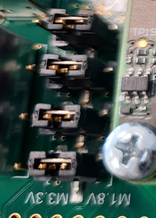
- Adjustable FPGA BANK supply voltages VCCIOA, VCCIOC ,VCCIOD (max. 2,7V, on TE0703 → 1.8V)
- Adjustable FPGA BANK supply voltages VCCIOA, VCCIOC ,VCCIOD (max. 2,7V, on TE0703 → 1.8V)
- General Purpose I/O
- D2 user LED on module (green)
| draw.io Diagram | ||||||||||||||||||||
|---|---|---|---|---|---|---|---|---|---|---|---|---|---|---|---|---|---|---|---|---|
|
TEG2000 + TE0703 Hardware Blockdiagram
Basic IOs<->FPGA connections are as following, Table 1:
| Component | Signal | FPGA Pin(Loc) | Function |
|---|---|---|---|
| Green LED D2(on module) | LED1 | IO_SB_B4 | custom LED |
| Clock | CLK_FPGA | IO_SB_A8 | singled ended 25MHz clock |
| Reset | MR | IO_EB_B0 | low active reset signal from S1 |
| Info |
|---|
Information on IO routing and FPGA pin connections can be found in the schematics. |
Board Power-Up
TEG2000 + TE0703 Hardware Setup and Power up
- Before connecting the Board to the PC, make sure to properly mount the module TEG2000 onto the carrier TE0703 via the B2B connector. It can only fit one way.
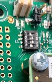
Check the Jumper settings. Bank Voltages to 1.8V. Caution! 3.3V setting could destroy the module. The description of the DIP-switches on the carrier can be found here.
- Use a Mini USB Cable to connect via USB to PC and a DC cable to connect to a power supply. The carrier TE0703 is supplied with 5V and 1A on the current limitation should suffice.
- Turning the board on, the LED D2 might be blinking if the module comes with a preloaded design. Otherwise the red DONE LED D3 would be ON if no FPGA design is loaded.
- The FPGA can be programmed with one of the example designs (e.g. from colognechip sample designs or our test board project) following the user guide ug1002 → Quick start or the video from Johannes 4GNU_Linux. To be able to program and use UART with the board on Windows OS, you need to install the right driver for the FTDI device on the carrier with the following zadig software. With linux as OS, programming should work out-of-the-box without touching the drivers.
Expand title zadig driver installation - For the programmer to work you need the zadig software https://zadig.akeo.ie/
- Download the exe file
- Execute it and click on Options → List all devices. Then Options → Ignore Hubs or Composite Parents
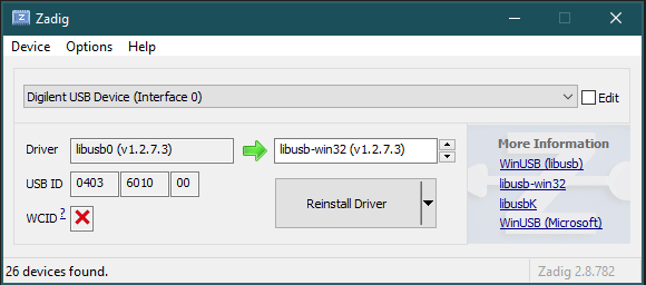
- From the device list choose the Digilent USB Device interface 0 / TE0703 device interface 0. Then select libusb-win32 any version and replace the driver for one interface only!
- After that, you should see your device in the device manager as follows:
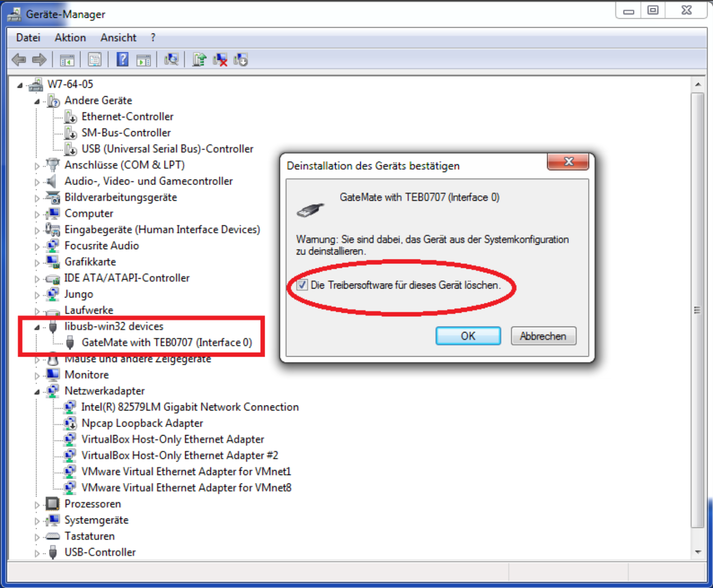
You can return the device to normal by deleting the driver.
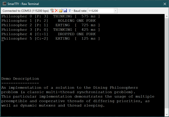
- If the QSPI Flash is loaded with our philosopher test design the green led blinks and you can connect to the board with a program like SmarTTY to see the output. Just open up SmarTTY and connect to with baud-rate of 115200. You may need to press the reset button to see the output.
Overview
Content Tools