Page History
...
Figure 1: TE0703 (REV 01).
Overview
Features
- VG96 Connectors (Mounting Holes and Solder Pads)
- Carrier Controller CPLD (Lattice LCMXO2-1200HC)
SD Card level-shifter
- Micro SD Card Connector
- LEDs
- Mini USB Connector FT2232H
- User Push Button
- RJ45 GbE Connector
- USB Host Connector
- Barrel jack for 5V Power Supply
- 4A High-Efficiency DC-DC Step-Down Converter for 3.3V Power Supply
- Trenz 4x5 Module Socket (3x Samtec LSHM Series Connectors)
- USB JTAG and UART Interface (FTDI FT2232H), compatible with Xilinx Tools
- DIP Switch
| Warning |
|---|
Note: TE0703 must be powered by a 5V power supply! |
User I/O Connectors
Note: VCCIO for FPGA banks is has no default fixed connection to power supply. Those the bank VCCIO must be supplied to externally, or optionally 0 ohm resistors can be soldered onto TE0703 to set fixed 3.3V voltages.
...
Example wiring that powers ALL banks with 3.3V - those connections should be present on the base board, in this drawing 3 banks are have VCCIO supplied over connector and 4th bank is connected to 3.3V with jumper J5.
TE0715-30 modification
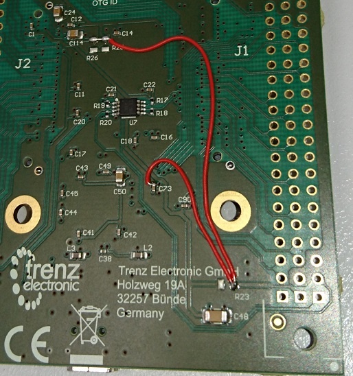
REMOVE jumper J5, add wires as on picture for VCCIO=1.8V for all banks.
UART
FT2232H USB interface Channel B is normally used as UART, in default CPLD configuration UART pins are routed to Module connector to location of default UART pins.
| FT2232H Channel B | B2B | TE0715 | TE0720 | TE0710 | TE0711 | TE0712 | TE0713 | TE0741 | Notes |
|---|---|---|---|---|---|---|---|---|---|
| TXD | JM1.92 | MIO14 | MIO14 | A8 | N17 | P16 | A10 | J21 | Module input |
| RXD | JM1.85 | MIO15 | MIO15 | B8 | R10 | U18 | C11 | G24 | Module output |
LEDS
Two LED's (those closer to mini-USB Connector) are connected to the 4x5 B2B Connector pins. Those LEDs can be controlled by FPGA Module.
...
Default function of the User LED's. Note the function of this LEDs is controlled by the CPLD and can be changed.
I2C Level Shifter
TE0703 has a I2C level shifter IC on-board, there are however no I2C devices on TE0703. Those pins that go through level shifter can be used I2C bus, or as GPIO.
| Net | B2B/Module | TE0715 | TE0720 | TE0710 | TE0711 | TE0712 | TE0713 | TE0741 | |
|---|---|---|---|---|---|---|---|---|---|
| SCL | JM1.95 | MIO10 | MIO10 | R10 | M13 | T21 | B9 | L22 | |
| SDA | JM1.93 | MIO11 | MIO11 | L18 | L18 | Y22 | A9 | K21 |
Micro SD Card Socket
The Micro SD Card Socket do not include a Card detect signal and Write Protect signal. It is not directly connected to the 4x5 B2B Connector pins, but through a SDIO port expander, TI TXS02612. This device is used for voltage translation, due to the different voltage levels between Micro SD Card and MIO Bank 501 on the Zynq 7000 . (The Micro SD Card is 3.3V, but the MIO Bank 501 is set to 1.8V.)
| Signal Name | Description | Net Name | B2B/Module | TE0715 | TE0720 |
|---|---|---|---|---|---|
| DATA[3] | Data | DAT3 | JM1.17 | MIO45 | MIO45 |
| DATA[2] | Data | DAT2 | JM1.19 | MIO44 | MIO44 |
| DATA[1] | Data | DAT1 | JM1.21 | MIO43 | MIO43 |
| DATA[0] | Data | DAT0 | JM1.23 | MIO42 | MIO42 |
| CMD | Command | CMD | JM1.25 | MIO41 | MIO41 |
| CLK | Clock | S_CLK | JM1.27 | MIO40 | MIO40 |
DIP Switch settings
| 4 | MODE = LOW | MODE = HIGH | Module "MODE" Pin level, select between boot-modes (SPI <> SD for Zynq modules) |
| 3 | Normal mode | CC Update mode | JTAG Select: fixed function can not be changed |
| 2 | |||
| 1 |
Function of MODE pin is module dependent!
Carrier Controller Update Mode
Carrier Controller JTAG port is enabled by setting switch 3 on DIP switch S2 on TE0703 to "OFF" position. This setting is only useful when updating Carrier Controller firmware! In this mode Module JTAG is not accessible.
Switch 3 on DIP switch S2 must be moved to "ON" position for normal operation! Otherwise the JTAG on the module would not be accessible at all.
Configuring B34 Bank Supply for TE0720 Zynq SoC Module
J5 Jumper can be used to power TE0720 bank 34 from TE0720 3.3V output rail. If J5 is installed TE0720 will boot also in the case bank 34 supply is not delivered from the VG96 /Pin headers. If TE0720 bank supply of 3.3V is required it is recommended to insert the jumper. Optionally, 3.3V or any other valid IO voltage can be supplied from the TE0703 pins.
Use with TE0715
| Warning |
|---|
Care should be taken with TE0715-30, all I/O should be set to 1.8V |
Backup Battery Supply (VBAT connector)
J7 provides two pins (+/-) to supply battery backup voltage to TE0720. If not required leave open.
Ensure to connect the supply battery to jumper J7 with correct polarity!
Revision History
REV 04
- corrected Pull up on U10
- PCB cosmetic changes
Document Change History
| date | revision | authors | description |
|---|---|---|---|
| 2014-02-12 | Work in progress | ||
All |
...
Overview
Content Tools