Page History
| HTML |
|---|
<!--
Template Revision 1.68
(HTML comments will be not displayed in the document, no need to remove them. For Template/Skeleton changes, increase Template Revision number. So we can check faster, if the TRM style is up to date).
--> |
| HTML |
|---|
<!--
General Notes:
If some section is CPLD firmware dependent, make a note and if available link to the CPLD firmware description. It's in the TE shop download area in the corresponding module -> revision -> firmware folder.
--> |
| HTML |
|---|
<!--
General Notes:
Designate all graphics and pictures with a number and a description. For example "Figure 1: TE07xx-xx Block Diagram" or "Table 1: Initial delivery state". "Figure x" and "Table x" have to be formatted to bold.
--> |
| HTML |
|---|
<!--
Link to the base folder of the module (remove de/ or en/ from the URL): for example:
https://shop.trenz-electronic.de/Download/?path=Trenz_Electronic/Modules_and_Module_Carriers/4x5/4x5_Carriers/TE0703/
--> |
| Scroll Ignore |
|---|
| Scroll pdf ignore | |
|---|---|
Table of Contents
|
Overview
The Trenz Electronic TE0782 is a high-performance, industrial-grade SoM (System on Module) with industrial temperature range based on Xilinx Zynq-7000 SoC (XC7Z035, XC7Z045 or XC7Z100).
These highly integrated modules with an economical price-performance-ratio have a form-factor of 8,5 x 8,5 cm and are available in several versions.
All parts cover at least industrial temperature range of -40°C to +85°C. The module operating temperature range depends on customer design and cooling solution. Please contact us for options and for modified PCB-equipping due increasing cost-performance-ratio and prices for large-scale order.
| HTML |
|---|
<!--
Use short link the Wiki Ressource page: for example:
http://trenz.org/te0782-info
List of available short links: https://wiki.trenz-electronic.de/display/CON/Redirects
--> |
| Scroll Only (inline) |
|---|
Refer to http://trenz.org/te0782-info for the current online version of this manual and other available documentation.
|
Key Features
- Xilinx Zynq-7000 XC7Z035, XC7Z045 or XC7Z100 SoC
- Rugged for shock and high vibration
- Large number of configurable I/Os are provided via rugged high-speed stacking strips
- Dual ARM Cortex-A9 MPCore
- 1 GByte RAM (32-Bit wide DDR3)
- 32 MByte QSPI Flash memory
- 2 x Hi-Speed USB2 ULPI transceiver PHY
- 2 x Gigabit (10/100/1000 Mbps) Ethernet transceiver PHY
- 4 GByte eMMC (optional up to 64 GByte)
- 2 x MAC-address EEPROMs
- Optional 2x 64 MByte HyperFLASH or 2x 8 MByte HyperRAM (max 2x 32 MByte HyperRAM)
- Temperature compensated RTC (real-time clock)
- Si5338A programmable quad PLL clock generator for GTX transceiver clocks
- Plug-on module with 3 x 160-pin high-speed strips
- 16 GTX high-performance transceiver
- 2x GT transceiver clock inputs
- 254 FPGA I/O's (125 LVDS pairs)
- On-board high-efficiency switch-mode DC-DC converters
- System management
- eFUSE bit-stream encryption
- AES bit-stream encryption
- Evenly-spread supply pins for good signal integrity
- User LED
Assembly options for cost or performance optimization available upon request.
Additional assembly options are available for cost or performance optimization upon request.
Block Diagram
| HTML |
|---|
<!--
Rules for all diagrams:
1. All diagrams are wrapped in the "Scroll Title" macro.
	- The title has to be named with the diagrams name
	- The anchor has the designation figure_x, whereby x is the number of the diagram

2. The Draw.IO diagram has to be inserted in the "Scroll Ignore" macro
	- Border has to be switched off in the macro edit
	- Toolbar has to be hidden in the macro edit

3. A PNG Export of the diagram has to be inserted in the "Scroll Only" macro

The workaround with the additional PNG of the diagram is necessary until the bug of the Scroll PDF Exporter, which cuts diagram to two pages, is fixed.


IMPORTANT NOTE: In case of copy and paste the TRM skeleton to a new Wiki page, delete the Draw.IO diagrams and the PNGs, otherwise due to the linkage of the copied diagrams every change in the TRM Skeleton will effect also in the created TRM and vice versa!

See page "Diagram Drawing Guidelines" how to clone an existing diagram as suitable template for the new diagram!

--> |
| Scroll Title | ||||||||||||||||||||||||||||||||
|---|---|---|---|---|---|---|---|---|---|---|---|---|---|---|---|---|---|---|---|---|---|---|---|---|---|---|---|---|---|---|---|---|
| ||||||||||||||||||||||||||||||||
|
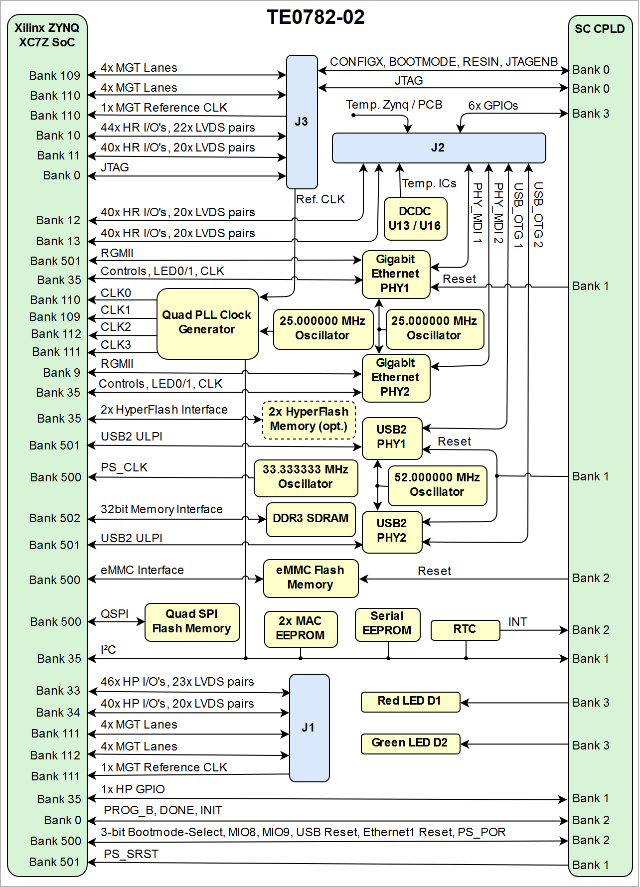
Main Components
| Scroll Title | ||||||||||||||||||||||||||||||||
|---|---|---|---|---|---|---|---|---|---|---|---|---|---|---|---|---|---|---|---|---|---|---|---|---|---|---|---|---|---|---|---|---|
| ||||||||||||||||||||||||||||||||
|
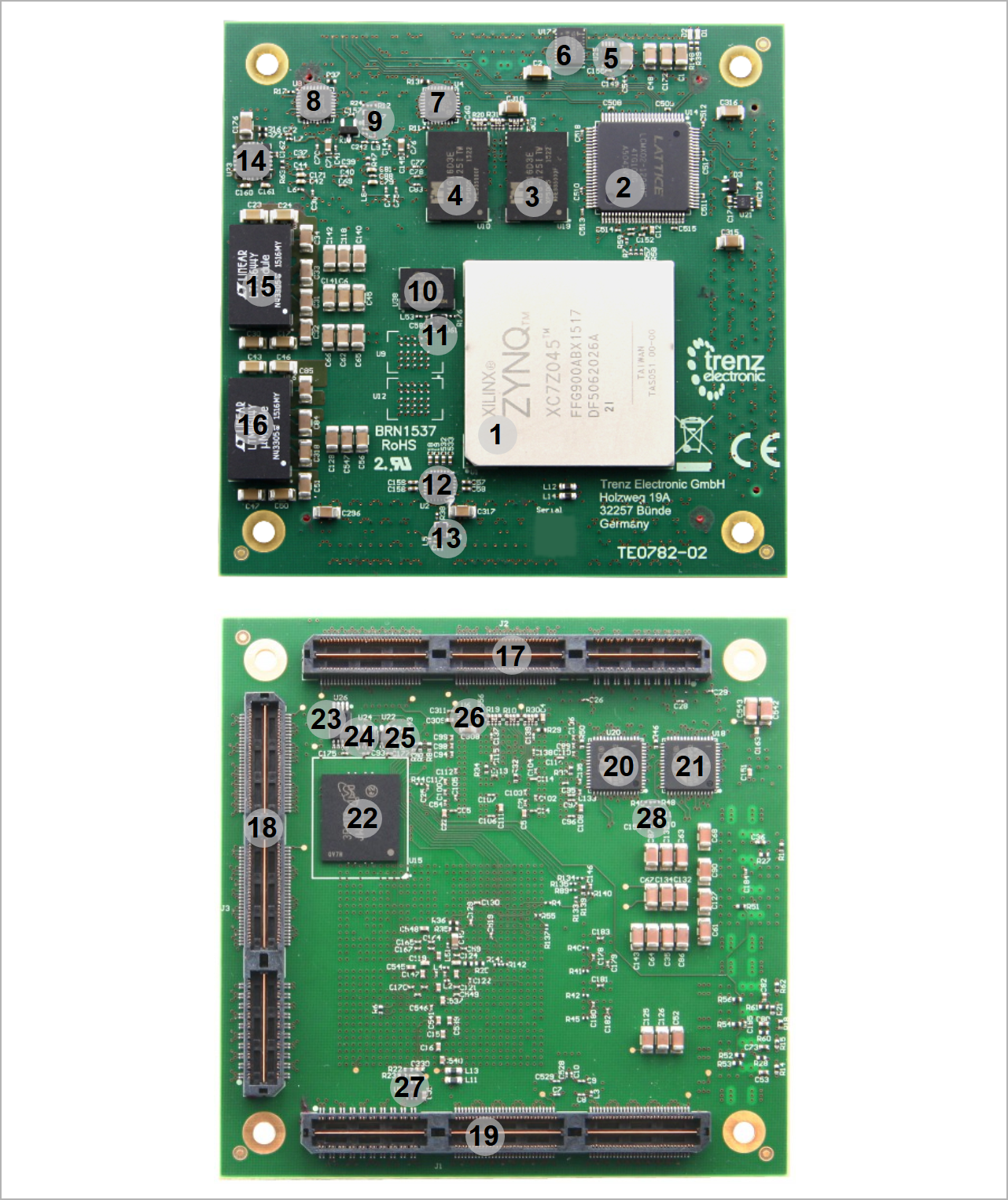
- Xilinx Zynq-7000 SoC, U1
- Lattice Semiconductor MachXO2 1200HC CPLD, U14
- 4Gbit DDR3L SDRAM, U19
- 4Gbit DDR3L SDRAM, U10
- I²C voltage translator, U25
- Intersil ISL12020MIRZ Real Time Clock, U17
- Microchip USB3320C USB PHY transceiver, U4
- Microchip USB3320C USB PHY transceiver, U8
- SiTime SiT8008 52.000000 MHz oscillator, U7
- 32 MByte QSPI Flash memory, U38
- SiTime SiT8008 33.333333 MHz oscillator, U61
- SI5338A programmable quad PLL clock generator, U2
- SiTime SiT8008 25.000000 MHz oscillator, U3
- TPS74801 LDO @1.5V, U23
- LT quad 4A PowerSoC DC-DC converter (@1.0V), U13
- LT quad 4A PowerSoC DC-DC converter (@3.3V, @1,8V, @1.2V_MGT, @1.0V_MGT), U16
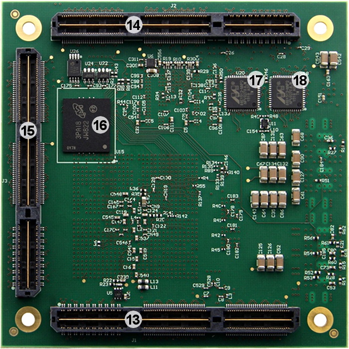
- Samtec ASP-122952-01 160-pin stacking strip (2 rows a 80 positions), J2
- Samtec ASP-122952-01 160-pin stacking strip (2 rows a 80 positions), J3
- Samtec ASP-122952-01 160-pin stacking strip (2 rows a 80 positions), J1
- Marvell Alaska 88E1512 Gigabit Ethernet PHY, 20
- Marvell Alaska 88E1512 Gigabit Ethernet PHY, U18
- Micron Technology 4 GByte eMMC, U15
- Microchip 128Kbit I²C EEPROM, U26
- Microchip 2Kbit I²C MAC EEPROM, U24
- Microchip 2Kbit I²C MAC EEPROM, U22
- TPS51206 DDR reference voltage and termination regulator, U6
- TPS799 LDO @1.8V_MGT, U5
- SiTime SiT8008 25.000000 MHz oscillator, U11
Initial Delivery State
| Storage device name | Content | Notes |
|---|---|---|
| 24LC128-I/ST | not programmed | User content |
24AA025E48 EEPROM's | User content not programmed | Valid MAC Address from manufacturer |
| Si5338A OTP Area | not programmed | - |
| eMMC Flash Memory | Empty, not programmed | Except serial number programmed by flash vendor |
SPI Flash OTP Area | Empty, not programmed | Except serial number programmed by flash vendor |
SPI Flash Quad Enable bit | Programmed | - |
SPI Flash main array | demo design | - |
| HyperFlash Memory | not programmed | - |
eFUSE USER | Not programmed | - |
eFUSE Security | Not programmed | - |
Table 1: Initial delivery state of programmable devices on the module
Boot Process
4 of the 7 boot mode strapping pins (MIO2 ... MIO8) of the Xilinx Zynq-7000 SoC device are hardware programmed on the board, 3 of them are set by the SC CPLD firmware. The boot strapping pins are evaluated by the Zynq device soon after the 'PS_POR' signal is deasserted to begin the boot process (see section "Boot Mode Pin Settings" of Xilinx manual UG585).
The TE0782 board is programmed in the SC CPLD firmware to boot initially from the on-board QSPI Flash memory U38. See section Bootmode in the TE0782 SC CPLD reference Wiki page.
The JTAG interface of the module is provided for storing the data to the QSPI Flash memory through the Zynq-7000 device.
Signals, Interfaces and Pins
Board to Board (B2B) I/Os
Zynq-7000 SoC's I/O banks signals connected to the B2B connectors:
| Bank | Type | B2B Connector | I/O Signal Count | Differential | Voltage | Notes |
|---|---|---|---|---|---|---|
10 | HR | J3 | 44 | 22 | User | Max voltage 3.3V |
11 | HR | J3 | 40 | 20 | User | Max voltage 3.3V |
| 12 | HR | J2 | 40 | 20 | User | Max voltage 3.3V |
13 | HR | J2 | 40 | 20 | User | Max voltage 3.3V |
33 | HP | J1 | 48 | 23 | User | Max voltage 1.8V |
| 34 | HP | J1 | 42 | 20 | User | Max voltage 1.8V |
Table 2: General overview of board to board I/O signals
For detailed information about the pin-out, please refer to the Pin-out table.
MGT Lanes
The Xilinx Zynq-7000 SoC used on the TE0782 module has 16 MGT transceiver lanes. All of them are wired directly to B2B connectors J1 and J3. MGT (Multi Gigabit Transceiver) lane consists of one transmit and one receive (TX/RX) differential pairs, four signals total per one MGT lane with data transmission rates up to 12.5Gb/s per lane (Xilinx GTX transceiver). Following table lists lane number, FPGA bank number, transceiver type, signal schematic name, board-to-board pin connection and FPGA pins connection:
Board to
| Bank | Type | Lane | Signal Name | B2B Pin | FPGA Pin |
|---|---|---|---|---|---|
| 109 | GTX | 0 |
|
|
|
| 1 |
|
|
| ||
| 2 |
|
|
| ||
| 3 |
|
|
| ||
| 110 | GTX | 0 |
|
|
|
| 1 |
|
|
| ||
| 2 |
|
|
| ||
| 3 |
|
|
| ||
| 111 | GTX | 0 |
|
|
|
| 1 |
|
|
| ||
| 2 |
|
|
| ||
| 3 |
|
|
| ||
| 112 | GTX | 0 |
|
|
|
| 1 |
|
|
| ||
| 2 |
|
|
| ||
| 3 |
|
|
|
Table 3: MGT lanes
There are 2 clock sources for the GTX transceivers. MGT_CLK1 and MGT_CLK4 are connected directly to B2B connector J3 and J1, so the clock can be provided by the carrier board. Clocks MGT_CLK0, MGT_CLK3, MGT_CLK5 and MGT_CLK6 are provided by the on-board clock generator (U2). As there are no capacitive coupling of the data and clock lines that are connected to the connectors, these may be required on the user’s PCB depending on the application.
| Bank | Type | Clock signal | Source | FPGA Pin | Notes |
|---|---|---|---|---|---|
| 109 | GTX | MGT_CLK3_P | U2, CLK3A | MGTREFCLK1P_109, AF10 | Supplied by on-board Si5338A |
| MGT_CLK3_N | U2, CLK3B | MGTREFCLK1N_109, AF9 | |||
| 110 | GTX | MGT_CLK0_P | U2, CLK2A | MGTREFCLK0P_110, AA8 | Supplied by on-board Si5338A |
| MGT_CLK0_N | U2, CLK2B | MGTREFCLK0N_110, AA7 | |||
| MGT_CLK1_N | J3-39 | MGTREFCLK1P_110, AC8 | Supplied by B2B connector J3 | ||
| MGT_CLK1_P | J3-37 | MGTREFCLK1N_110, AA7 | |||
| 111 | GTX | MGT_CLK4_N | J1-40 | MGTREFCLK0P_111, U8 | Supplied by B2B connector J1 |
| MGT_CLK4_P | J1-38 | MGTREFCLK0N_111, U7 | |||
| MGT_CLK5_P | U2, CLK1A | MGTREFCLK1P_111, W8 | Supplied by on-board Si5338A | ||
| MGT_CLK5_N | U2, CLK1B | MGTREFCLK1N_111, W7 | |||
| 112 | GTX | MGT_CLK6_P | U2, CLK0A | MGTREFCLK0P_112, N8 | Supplied by on-board Si5338A |
| MGT_CLK6_N | U2, CLK0B | MGTREFCLK0N_112, N7 |
Table 4: MGT reference clock sources
JTAG Interface
JTAG access to the Xilinx Zynq-7000 is provided through B2B connector J3.
JTAG Signal | B2B Connector Pin |
|---|---|
| TMS | J3-142 |
| TDI | J3-147 |
| TDO | J3-148 |
| TCK | J3-141 |
Table 5: Zynq JTAG interface signals
JTAG access to the LCMXO2-1200HC System Controller CPLD U14 is provided through B2B connector J3.
JTAG Signal | B2B Connector Pin |
|---|---|
| M_TMS | J3-82 |
| M_TDI | J3-87 |
| M_TDO | J3-88 |
| M_TCK | J3-81 |
Table 6: System Controller CPLD JTAG interface signals
Pin J3-136 'JTAGENB' of B2B connector J3 is used to access the JTAG interface of the SC CPLD. Set high to program the System Controller CPLD via JTAG interaface.
System Controller CPLD I/O Pins
Special purpose pins are connected to System Controller CPLD and have following default configuration:
| Pin Name | Direction | Function | Default Configuration |
|---|---|---|---|
| BOOTMODE | in | in | signal forwarded to MIO9 and currently used as UART RX line |
| CONFIGX | in | out | signal forwarded to MIO8 and currently used as UART TX line |
| RESIN | in | nRESET | external Board Reset |
| M_TDO | out | CPLD JTAG interface | - |
| M_TDI | in | ||
| M_TCK | in | ||
| M_TMS | in | ||
| JTAGENB | in | enable JTAG | pull high for programming SC CPLD firmware |
| I2C_SCL | in / out | I²C data line | I²C bus of board |
| I2C_SDA | in | I²C clock | |
| CPLD_IO | in / out | user GPIO | currently not used |
| ETH1_RESET | out | reset GbE PHY U18 | see current SC CPLD firmware |
| OTG-RST | out | reset USB2 PHYs U4 and U8 | see current SC CPLD firmware |
| RTC_INT | in | interrupt | interrupt from RTC |
| PS_SRST | out | Zynq control signal | reset PS of Zynq-7000 SoC |
| DONE | in | PL configuration completed | |
| PROG_B | out | PL configuration reset signal | |
| INIT | in | Low active FPGA initialization pin or configuration error signal | |
| PS_POR | out | PS power-on reset | |
| BM0/MIO5 | out | Bootmode Pins currently configured in SC CPLD firmare to boot from QSPI Flash | |
| BM2/MIO4 | out | ||
| BM3/MIO2 | out | ||
| MIO8 | in | user MIO pins | currently used as UART interface |
| MIO9 | out | ||
| MMC_RST | out | Reset MMC Flash | see current SC CPLD firmware |
| ETH1-RESET33 | in | reset GbE PHY U18 | reset signal from Zynq-7000 level shifted to 1.8V |
| OTG-RST33 | in | reset USB2 PHYs | reset signal from Zynq-7000 level shifted to 1.8V |
| LED1 ... LED2 | out | LED status signal | see current CPLD firmware |
| CPLD_GPIO0 ... CPLD_GPIO5 | in / out | user GPIO | currently not used |
| EN_1V | out | Power control | enable signal DCDC U13 '1V' |
| PG_1V | in | power good signal DCDC U13 '1V' | |
| EN_1.0V_MGT | out | enable signal DCDC U16 '1.0V_MGT' | |
| PG_1.0V_MGT | in | power good signal DCDC U16 '1.0V_MGT' | |
| EN_1.2V_MGT | out | enable signal DCDC U16 '1.2V_MGT' | |
| PG_1.2V_MGT | in | power good DCDC U16 '1.2V_MGT' | |
| EN_1.8V | out | enable signal DCDC U16 '1.8V' | |
| PG_1.8V | in | power good signal DCDC U16 '1.8V' | |
| EN_3.3V | out | enable signal DCDC U16 '3.3V' | |
| PG_3.3V | in | power good signal DCDC U16 '3.3V' | |
| PG_1V5 | in | power good signal DCDC U23 '1.5V' |
Table 7: System Controller CPLD special purpose pins.
See also TE0782 CPLD reference Wiki page.
Default PS MIO Mapping
| MIO | Function | Connected to |
|---|---|---|
| 0 | USB2 PHYs Reset | SC CPLD (used as level translator) |
| 1 | QSPI0 | SPI Flash-CS |
| 2 | QSPI0 | SPI Flash-DQ0 |
| 3 | QSPI0 | SPI Flash-DQ1 |
| 4 | QSPI0 | SPI Flash-DQ2 |
| 5 | QSPI0 | SPI Flash-DQ3 |
| 6 | QSPI0 | SPI Flash-SCK |
| 7 | Ethernet PHY1 Reset | SC CPLD (used level translator) |
| 8 | UART TX | output, muxed to B2B by the SC CPLD |
| 9 | UART RX | input, muxed to B2B by the SC CPLD |
| 10 | SDIO1 D0 | eMMC DAT0 |
| 11 | SDIO1 CMD | eMMC CMD |
| 12 | SDIO1 CLK | eMMC CLK |
| 13 | SDIO1 D1 | eMMC DAT1 |
| 14 | SDIO1 D2 | eMMC DAT2 |
| 15 | SDIO1 D3 | eMMC DAT3 |
| 16..27 | ETH0 | Ethernet RGMII PHY |
| 28..39 | USB0 | USB0 ULPI PHY |
| 40...51 | USB1 | USB1 ULPI PHY |
| 52 | ETH0 MDC | - |
| 53 | ETH0 MDIO | - |
Table 8: Zynq PS MIO mapping
Gigabit Ethernet
The TE0782 is equipped with two Marvell Alaska 88E1512 Gigabit Ethernet PHYs (U18 (ETH1) and U20 (ETH2)). The transceiver PHY of ETH1 is connected to the Zynq PS Ethernet GEM0. The I/O Voltage is fixed at 1.8V for HSTL signaling. The reference clock input for both PHYs is supplied from an on board 25MHz oscillator (U11), the 125MHz output clock of both PHYs are connected to Zynq's PL bank 35.
ETH1 PHY connection:
| PHY PIN | Zynq PS / PL | System Controller CPLD | Notes |
|---|---|---|---|
| MDC/MDIO | MIO52, MIO53 | - | - |
| LED0 | Bank 35, Pin B12 | - | - |
| LED1 | Bank 35, Pin C12 | - | - |
| Interrupt | Bank 35, Pin A15 | - | - |
| CONFIG | Bank 35, Pin F14 | - | When pin connected to GND, PHY Address is strapped to 0x00 by default |
| RESETn | - | Pin 53 | ETH1_RESET33 (MIO7) -> SC CPLD -> ETH1_RESET |
| RGMII | MIO16..MIO27 | - | |
| MDI | - | - | on B2B J2 connector |
Table 9: General overview of the Gigabit Ethernet1 PHY signals
ETH2 PHY connection:
| PHY PIN | Zynq PS / PL | System Controller CPLD | Notes |
|---|---|---|---|
| MDC/MDIO | Bank 35, Pin C17/B17 | - | - |
| LED0 | Bank 35, Pin K15 | - | - |
| LED1 | Bank 35, Pin B16 | - | - |
| Interrupt | Bank 35, Pin A17 | - | - |
| CONFIG | Bank 35, Pin E15 | - | When pin connected to GND, PHY Address is strapped to 0x00 by default |
| RESETn | Bank 35, Pin B15 | - | - |
| RGMII | Bank 9 | - | - |
| MDI | - | - | on B2B J2 connector |
Table 10: General overview of the Gigabit Ethernet2 PHY signals
USB Interface
The TE0782 is equipped with two USB PHY's USB3320 from Microchip (U4 (USB0) and U8 (USB1)). The ULPI interface of USB0 is connected to the Zynq PS USB0, ULPI interface of USB1 to Zynq PS USB1. The I/O Voltage is fixed at 1.8V.
The reference clock input of both PHY's is supplied from an on board 52MHz oscillator (U7).
USB0 PHY connection:
| PHY Pin | Zynq PS / PL | CPLD | B2B Connector J2 | Notes |
|---|---|---|---|---|
| ULPI | MIO28..39 | - | - | Zynq USB0 MIO pins are connected to the PHY |
| REFCLK | - | - | - | 52MHz from on board oscillator (U7) |
| REFSEL[0..2] | - | - | - | 000 GND, select 52MHz reference Clock |
| RESETB | MIO0 | OTG_RESET33 | - | OTG_RESET33 -> SC CPLD -> OTG_RESET |
| CLKOUT | MIO36 | - | - | Connected to 1.8V selects reference clock operation mode |
| DP,DM | - | - | USB1_D_P, USB1_D_N | USB Data lines |
| CPEN | - | - | VBUS1_V_EN | External USB power switch active high enable signal |
| VBUS | - | - | USB1_VBUS | Connect to USB VBUS via a series resistor. Check reference schematic. |
| ID | - | - | OTG1_ID | For an A-Device connect to ground, for a B-Device left floating |
Table 11: General overview of the USB0 PHY signals
USB1 PHY connection:
| PHY Pin | Zynq PS / PL | CPLD | B2B Connector J2 | Notes |
|---|---|---|---|---|
| ULPI | MIO40..51 | - | - | Zynq USB1 MIO pins are connected to the PHY |
| REFCLK | - | - | - | 52MHz from on board oscillator (U7) |
| REFSEL[0..2] | - | - | - | 000 GND, select 52MHz reference Clock |
| RESETB | MIO0 | OTG_RESET33 | - | OTG_RESET33 -> SC CPLD -> OTG_RESET |
| CLKOUT | MIO48 | - | - | Connected to 1.8V selects reference clock operation mode |
| DP,DM | - | - | USB2_D_P, USB2_D_N | USB Data lines |
| CPEN | - | - | VBUS2_V_EN | External USB power switch active high enable signal |
| VBUS | - | - | USB2_VBUS | Connect to USB VBUS via a series resistor. Check reference schematic. |
| ID | - | - | OTG2_ID | For an A-Device connect to ground, for a B-Device left floating |
Table 12: General overview of the USB1 PHY signals
I2C Interface
The on-board I2C components are connected to bank 35 pins L15 (I2C_SDA) and L14 (I2C_SCL).
I2C addresses for on-board components:
| Device | IC | Designator | I2C-Address | Notes |
|---|---|---|---|---|
| EEPROM | 24LC128-I/ST | U26 | 0x53 | user data |
| EEPROM | 24AA025E48T-I/OT | U22 | 0x50 | MAC address EEPROM |
| EEPROM | 24AA025E48T-I/OT | U24 | 0x51 | MAC address EEPROM |
| RTC | ISL12020MIRZ | U17 | 0x6F | Temperature compensated real time clock |
| Battery backed RAM | ISL12020MIRZ | U17 | 0x57 | Integrated in RTC |
| PLL | SI5338A-B-GMR | U2 | 0x70 | - |
| SC CPLD | LCMXO2-1200HC-4TG100I | U14 | user | - |
Table 13: Address table of the I2C bus slave devices
Pin Definitions
Pins with names ending with _VRN and _VRP are connected to Zynq PL HP bank special purpose pins VRN/VRP and can be routed to DCI calibration resistors on the baseboard. Otherwise they are usable as general purpose I/Os.
Bank 35 has 100 ohm DCI calibration resistors installed, it is also possible to "borrow" the DCI calibration from bank 35 for banks 34 and 33. For more detailed information about the DCI check Xilinx documentation.
On-board Peripherals
System Controller CPLD
The System Controller CPLD (U14) is provided by Lattice Semiconductor LCMXO2-1200HC (MachXO2 product family). It is the central system management unit with module specific firmware installed to monitor and control various signals of the FPGA, on-board peripherals, I/O interfaces and module as a whole.
See also TE0782 CPLD reference Wiki page.
eMMC Flash Memory
eMMC Flash memory device (U15) is connected to the Zynq PS MIO bank 500 pins MIO10..MIO15. eMMC chips MTFC4GMVEA-4M IT (Flash NAND-IC 2x 16 Gbit) is used with 4 GByte of memory density.
DDR3L Memory
By default TE0782-02 module has two 16-bit wide IM (Intelligent Memory) IM4G16D3FABG-125I DDR3L SDRAM (DDR3-1600 Speedgrade) chips (U10, U19) arranged into 32-bit wide memory bus providing total of 1 GBytes of on-board RAM.
Quad SPI Flash Memory
Two quad SPI compatible serial bus flash memory for FPGA configuration file storage is provided by Spansion S25FL256SAGBHI20 (U38) with 256 Mbit (32 MByte) memory density. After configuration completes the remaining free memory can be used for application data storage. All four SPI data lines are connected to the FPGA allowing x1, x2 or x4 data bus widths to be used. The maximum data transfer rate depends on the bus width and clock frequency.
Gigabit Ethernet PHYs
On-board Gigabit Ethernet PHYs (U18, U20) are provided by Marvell Alaska 88E1512. The Ethernet PHYs' RGMII interfaces are connected to the Zynq's PS MIO bank 501 and to PL bank 9. I/O voltage is fixed at 1.8V for HSTL signaling. The reference clock input of both PHYs is supplied from an on-board 25.000000 MHz oscillator (U11).
High-speed USB ULPI PHYs
Hi-speed USB ULPI PHYs (U4. U8) are provided with USB3320 from Microchip. The ULPI interfaces are connected to the Zynq PS USB0 and USB1 via MIO28..51, bank 501 (see also section USB interface). The I/O voltage is fixed at 1.8V and PHY reference clock input is supplied from the on-board 52.000000 MHz oscillator (U7).
MAC Address EEPROMs
Two Microchip 24AA025E48 serial EEPROMs (U22, U24) contain globally unique 48-bit node address, which are compatible with EUI-48(TM) specification. The devices are organized as two blocks of 128 x 8 Kbit memory. One of the blocks stores the 48-bit node address and is write protected, the other block is available for application use. The MAC address EEPROMS areaccessible over I2C bus (see also section I²C interface).
Configuration EEPROM
The TE0782 board contains one EEPROM (U26) for configuration and general user purposes. The EEPROMs is provided by Microchip 24LC128-I/ST with 128 KBit memory density, the EEPROM is areaccessible over I2C bus (see also section I²C interface).
Programmable Clock Generator
There is a Silicon Labs I2C programmable clock generator Si5338A (U2) chip on-board. It's output frequencies can be programmed using the I2C bus address 0x70 or 0x71. Default address is 0x70, IN4/I2C_LSB pin must be set to high for address 0x71.
A 25.000000 MHz oscillator (U3) is connected to the pin IN3 and is used to generate the output clocks. The output voltage of the oscillator is provided by the 1.8V power rail, thus making output frequency available as soon as 1.8V is present. All 4 of the Si5338 clock outputs are connected to the MGT banks of the Zynq device. It is possible to use the clocks connected to the GTR bank in the user's logic design. This is achieved by instantiating a IBUFDSGTE buffer in the design.
Once running, the frequency and other parameters can be changed by programming the device using the I2C bus connected between the FPGA (master) and clock generator (slave). For this, proper I2C bus logic has to be implemented in FPGA.
| Signal | Frequency | Notes |
|---|---|---|
| IN1/IN2 | user | External clock signal supply from B2B connector J3, pins J3-38 / J3-40 |
IN3 | 25.000000 MHz | Fixed input clock signal from reference clock generator SiT8008BI-73-18S-25.000000E (U3) |
| IN4 | - | LSB of the default I2C address, wired to ground mean address is 0x70 |
IN5 | - | Not connected |
IN6 | - | Wired to ground |
| CLK0 A/B | - | reference clock 0 of Bank 112 GTX |
CLK1 A/B | - | reference clock 1 of Bank 111 GTX |
CLK2 A/B | - | reference clock 0 of Bank 110 GTX |
| CLK3 A/B | - | reference clock 1 of Bank 109 GTX |
Table 14: General overview of the on-board quad clock generator I/O signals
Oscillators
The module has following reference clock signals provided by on-board oscillators and external source from carrier board:
| Clock Source | Schematic Name | Frequency | Clock Destination |
|---|---|---|---|
| SiTime SiT8008AI oscillator, U61 | PS_CLK | 33.333333 MHz | Zynq SoC U1, pin A22 |
| SiTime SiT8008BI oscillator, U21 | - | 25.000000 MHz | Quad PLL clock generator U2, pin 3 |
| SiTime SiT8008AI oscillator, U7 | - | 52.000000 MHz | USB2 PHYs U4 and U8, pin 26 |
| SiTime SiT8008BI oscillator, U11 | - | 25.000000 MHz | GbE PHYs U18 and U20, pin 34 |
Table 15: Reference clock signals
On-board LEDs
| LED | Color | Connected to | Description and Notes |
|---|---|---|---|
| D1 | Red | System Controller CPLD U14, bank 3 | Exact function is defined by SC CPLD firmware |
| D2 | Green | System Controller CPLD U14, bank 3 |
Table 16: On-board LEDs
Power and Power-on Sequence
Power Supply
Power supply with minimum current capability of 4A for system startup is recommended.
Power Consumption
| Power Input | Typical Current |
|---|---|
| VIN | TBD* |
| C3.3V | TBD* |
Table 17: Power consumption
* TBD - To Be Determined soon with reference design setup.
| Warning |
|---|
| To avoid any damage to the module, check for stabilized on-board voltages should be carried out (i.e. power good and enable signals) before powering up any Zynq's I/O bank voltages VCCO_x. All I/Os should be tri-stated during power-on sequence. |
Power Distribution Dependencies
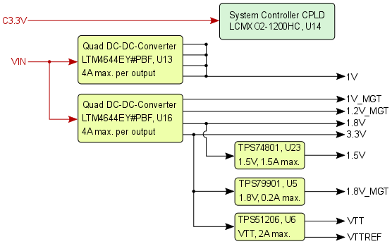
The Trenz TE0782 SoM is equipped with two quad DC-DC voltage regulators to generate required on-board voltage levels 1V, 3.3V, 1.8V, 1.2V_MGT, 1V_MGT. Additional voltage regulators are used to generate voltages 1.5V, VTT, VTTREF and 1.8V_MGT.
The power supply voltage 'C3.3V' of System Controller CPLD of the SoM have to be externally supplied with 3.3V nominal.
There are following dependencies how the initial voltages of the power rails on the B2B connectors are distributed to the on-board DC-DC converters, which power up further DC-DC converters and the particular on-board voltages:
| Scroll Title | ||||||||||||||||||||||||||||||||
|---|---|---|---|---|---|---|---|---|---|---|---|---|---|---|---|---|---|---|---|---|---|---|---|---|---|---|---|---|---|---|---|---|
| ||||||||||||||||||||||||||||||||
|
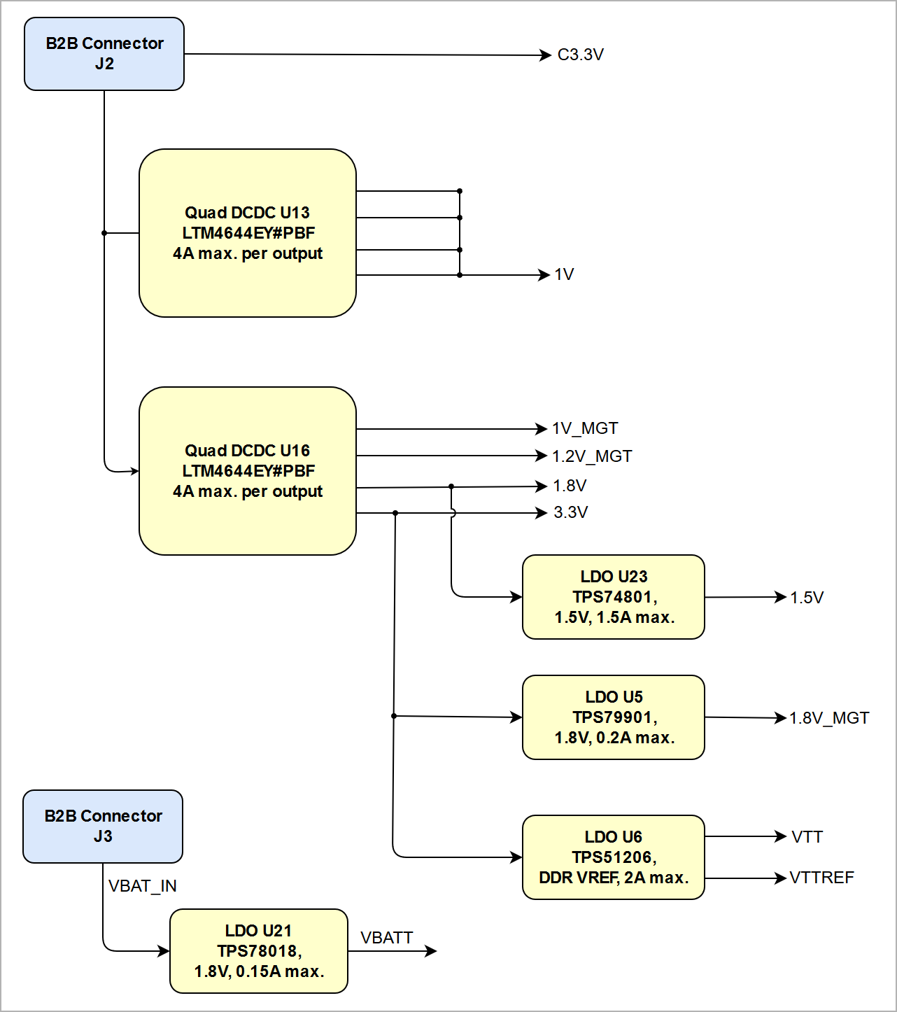
See also Xilinx datasheet DS191 for additional information. User should also check related base board documentation when intending base board design for TE0782 module.
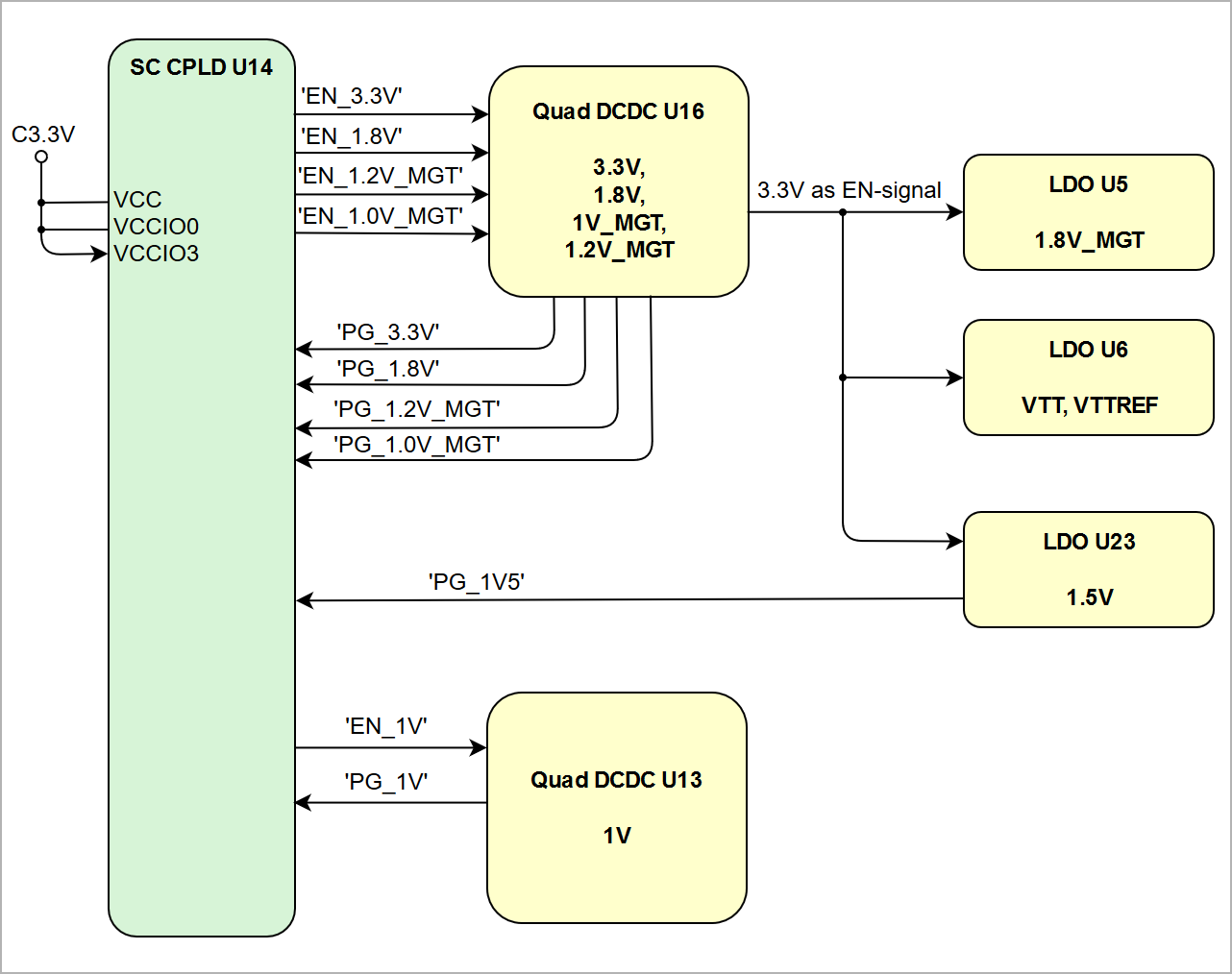
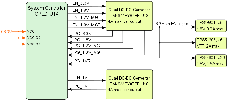
Power-On Sequence
Power-on sequence is handled by the System Controller CPLD using "Power good"-signals from the voltage regulators:
| Scroll Title | ||||||||||||||||||||||||||||||||
|---|---|---|---|---|---|---|---|---|---|---|---|---|---|---|---|---|---|---|---|---|---|---|---|---|---|---|---|---|---|---|---|---|
| ||||||||||||||||||||||||||||||||
|
Power Rails
| Power Rail Name on B2B Connector | J1 Pins | J2 Pins | J3 Pins | Direction | Notes |
|---|---|---|---|---|---|
| VIN | - | 165, 166, 167, 168 | - | Input | external power supply voltage |
| C3.3V | - | 147, 148 | - | Input | external 3.3V power supply voltage |
| 3.3V | - | 111, 112, 123, 124, 135 136 169, 170, 171, 172 | - | Output | internal 3.3V voltage level |
| 1.8V | 169, 170, 171, 172 | - | - | Output | internal 1.8V voltage level |
| VCCIO_10 | - | - | 99, 100 | Input | high range I/O bank voltage |
| VCCIO_11 | - | - | 159, 160 | Input | high range I/O bank voltage |
| VCCIO_12 | - | 159, 160 | - | Input | high range I/O bank voltage |
| VCCIO_13 | - | 99, 100 | - | Input | high range I/O bank voltage |
| VCCIO_33 | 99, 100 | - | - | Input | high performance I/O bank voltage |
| VCCIO_34 | 159, 160 | - | - | Input | high performance I/O bank voltage |
| VBAT_IN | - | - | 124 | Input | backup battery voltage |
Table 18: Module power rails
Bank Voltages
| Bank | Schematic Name | Voltage | Range | Notes |
|---|---|---|---|---|
| 0 | - | 3.3 V | - | FPGA configuration |
| 502 | - | 1.5 V | - | DDR3-RAM port |
| 109 / 110 / 111 / 112 | - | 1.2 V | - | MGT |
| 500 / 501 | - | 3.3 V | - | MIO banks |
| 9 (HR) | - | 1.8 V | 1.2V to 3.3V | ETH2 RGMII |
| 10 (HR) | VCCIO_10 | user | 1.2V to 3.3V | - |
| 11 (HR) | VCCIO_11 | user | 1.2V to 3.3V | - |
| 12 (HR) | VCCIO_12 | user | 1.2V to 3.3V | - |
| 13 (HR) | VCCIO_13 | user | 1.2V to 3.3V | - |
| 33 (HP) | VCCIO_33 | user | 1.2V to 1.8V | - |
| 34 (HP) | VCCIO_34 | user | 1.2V to 1.8V | - |
| 35 (HP) | - | 1.8 V | 1.2V to 1.8V | Hyper-RAM, Ethernet, I²C |
Table 19: Module I/O bank voltages
See Xilinx Zynq-7000 datasheet DS191 for the voltage ranges allowed.
Board to Board Connectors
Include Page 8.5 x 8.5 SoM QSH and QTH B2B Connectors 8.5 x 8.5 SoM QSH and QTH B2B Connectors
Variants Currently In Production
| Trenz shop TE0782 overview page | |
|---|---|
| English page | German page |
Technical Specifications
Absolute Maximum Ratings
Parameter | Min | Max | Units | Notes |
|---|---|---|---|---|
VIN supply voltage | -0.3 | 15 | V | LTM4644 datasheet |
| C3.3V supply voltage | -0.3 | 3.6 | V | LTM4644 datasheet |
| VBAT supply voltage | -0.3 | 6 | V | TPS780180 datasheet |
| PS I/O supply voltage, VCCO_PSIO | -0.5 | 3.6 | V | Xilinx document DS191 |
| PS I/O input voltage | -0.4 | VCCO_PSIO + 0.55 | V | Xilinx document DS191 |
| HP I/O bank supply voltage, VCCO | -0.5 | 2.0 | V | Xilinx document DS191 |
| HP I/O bank input voltage | -0.55 | VCCO + 0.55 | V | Xilinx document DS191 |
| HR I/O bank supply voltage, VCCO | -0.5 | 3.6 | V | Xilinx document DS191 |
| HR I/O bank input voltage | -0.55 | VCCO + 0.55 | V | Xilinx document DS191 |
| Reference Voltage pin | -0.5 | 2 | V | Xilinx document DS191 |
| Differential input voltage | -0.4 | 2.625 | V | Xilinx document DS191 |
| MGT reference clocks absolute input voltage | -0.5 | 1.32 | V | Xilinx document DS191 |
| MGT absolute input voltage | -0.5 | 1.26 | V | Xilinx document DS191 |
Voltage on SC CPLD pins | -0.5 | 3.75 | V | Lattice Semiconductor MachXO2 datasheet |
Storage temperature | -40 | +85 | °C | See eMMC MTFC4GMVEA datasheet |
Table 20: Module absolute maximum ratings
Recommended Operating Conditions
| Parameter | Min | Max | Units | Notes |
|---|---|---|---|---|
| VIN supply voltage | 11.4 | 12.6 | V | LTM4644 datasheet, 12V nominal |
| C3.3V supply voltage | 3.3 | 3.465 | V | LCMXO2-256HC, LTM4644 datasheet |
| VBAT supply voltage | 2.2 | 5.5 | V | TPS780180 datasheet |
| PS I/O supply voltage, VCCO_PSIO | 1.710 | 3.465 | V | Xilinx document DS191 |
| PS I/O input voltage | –0.20 | VCCO_PSIO + 0.20 | V | Xilinx document DS191 |
| HP I/O banks supply voltage, VCCO | 1.14 | 1.89 | V | Xilinx document DS191 |
| HP I/O banks input voltage | -0.20 | VCCO + 0.20 | V | Xilinx document DS191 |
| HR I/O banks supply voltage, VCCO | 1.14 | 3.465 | V | Xilinx document DS191 |
| HR I/O banks input voltage | -0.20 | VCCO + 0.20 | V | Xilinx document DS191 |
| Differential input voltage | -0.2 | 2.625 | V | Xilinx document DS191 |
| Voltage on SC CPLD pins | -0.3 | 3.6 | V | Lattice Semiconductor MachXO2 datasheet |
| Operating Temperature Range | -40 | 85 | °C | Xilinx document DS191, industrial grade Zynq temperarure range |
Table 21: Recommended operating conditions
Module operating temperature range depends also on customer design and cooling solution. Please contact us for options.
| Note |
|---|
| See Xilinx datasheet DS191 for more information about absolute maximum and recommended operating ratings for the Zynq-7000 chips. |
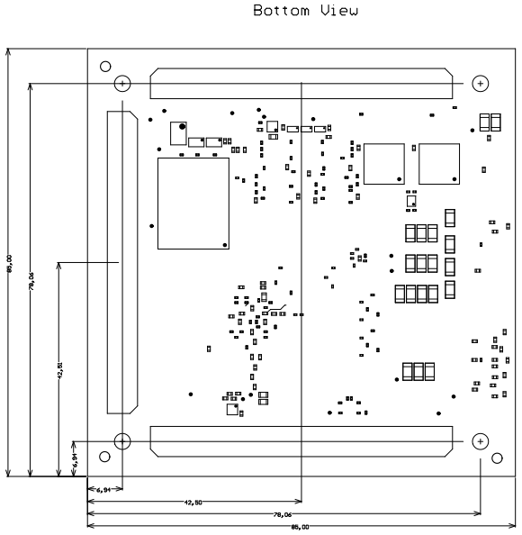
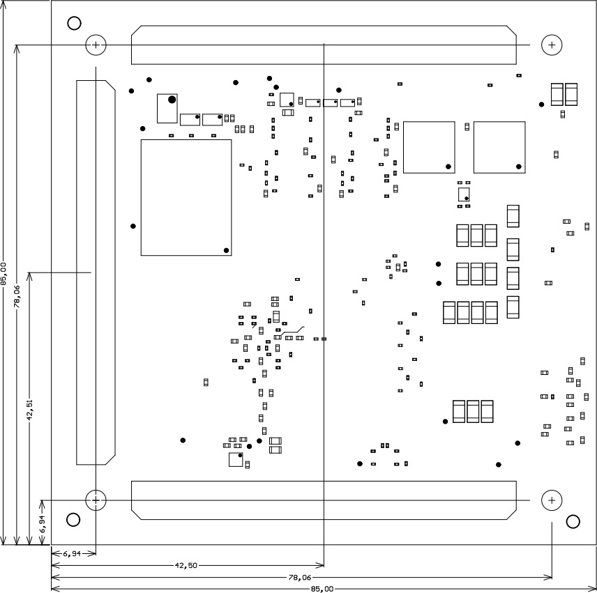
Physical Dimensions
Module size: 85 mm × 85 mm. Please download the assembly diagram for exact numbers.
Mating height with standard connectors: 5 mm
PCB thickness: 1.7 mm
All dimensions are shown in millimeters.
| Scroll Title | ||||
|---|---|---|---|---|
| ||||
|
Revision History
Hardware Revision History
| Date | Revision | Notes | PCN Link | Documentation Link |
|---|---|---|---|---|
| - | 02 | current available board revision | - | TE0782-02 |
| 2015-05-27 | 01 | Prototype only | - | - |
Table 22: Hardware revision history table
| Scroll Title | ||||
|---|---|---|---|---|
| ||||
|
Document Change History
| HTML |
|---|
<!--
Generate new entry:
1.add new row below first
2.Copy "Page Information Macro(date)" Macro-Preview, Metadata Version number, Author Name and description to the empty row. Important Revision number must be the same as the Wiki document revision number
3.Update Metadata = "Page Information Macro (current-version)" Preview+1 and add Author and change description.
--> |
| Date | Revision | Contributors | Description | ||||||||||||||||||||||||||
|---|---|---|---|---|---|---|---|---|---|---|---|---|---|---|---|---|---|---|---|---|---|---|---|---|---|---|---|---|---|
|
|
|
| ||||||||||||||||||||||||||
| 2018-07-20 | v.33 | John Hartfiel |
| ||||||||||||||||||||||||||
2018-07-19 | v.32 | Ali Naseri |
| ||||||||||||||||||||||||||
| 2018-05-15 | v.22 | Ali Naseri |
| ||||||||||||||||||||||||||
| 2018-01-31 | Ali Naseri |
| |||||||||||||||||||||||||||
| 2017-06-07 | Jan Kumann |
| |||||||||||||||||||||||||||
| 2017-05-23 | v.13 | Jan Kumann |
| ||||||||||||||||||||||||||
| 2017-01-24 | v.12 | Ali Naseri |
| ||||||||||||||||||||||||||
| 2016-06-27 | v.10 | Ali Naseri, Jan Kumann |
| ||||||||||||||||||||||||||
| -- | all |
|
|
...
Download PDF version of this document.
| Scroll pdf ignore | |
|---|---|
Table of Contents
|
Overview
| Scroll Only (inline) |
|---|
Refer to https://wiki.trenz-electronic.de/display/PD/TE0782+TRM for online version of this manual and the rest of available documentation.
|
The Trenz Electronic TE0782 is a high-performance, industrial-grade SoM (System on Module) with industrial temperature range based on Xilinx Zynq-7000 SoC (XC7Z035, XC7Z045 or XC7Z100).
These highly integrated modules with an economical price-performance-ratio have a form-factor of 8,5 x 8,5 cm and are available in several versions.
All parts cover at least industrial temperature range of -40°C to +85°C. The module operating temperature range depends on customer design and cooling solution. Please contact us for options and for modified PCB-equipping due increasing cost-performance-ratio and prices for large-scale order.
Key Features
- Xilinx Zynq-7 XC7Z035, XC7Z045 or XC7Z100 SoC
- Rugged for shock and high vibration
- Large number of configurable I/Os are provided via rugged high-speed stacking strips
- Dual ARM Cortex-A9 MPCore
- 1 GByte RAM (32-Bit wide DDR3)
- 32 MByte QSPI Flash memory
- 2 x Hi-Speed USB2.0 ULPI transceiver PHY
- 2 x Gigabit (10/100/1000 Mbps) Ethernet transceiver PHY
- 4 GByte eMMC (optional up to 64 GByte)
- 2 x MAC-address EEPROMs
- Optional 2 x 8 MByte HyperRAM (max 2 x 32 MByte) or optional 2 x 64 MByte HyperFLASH
- Temperature compensated RTC (real-time clock)
- Si5338 PLL for GTX transceiver clocks
- Plug-on module with 3 x 160-pin high-speed strips
- 16 GTX high-performance transceiver
- GT transceiver clock inputs
- 254 FPGA I/O's (125 LVDS pairs)
- On-board high-efficiency switch-mode DC-DC converters
- System management
- eFUSE bit-stream encryption
- AES bit-stream encryption
- Evenly-spread supply pins for good signal integrity
- User LED
Assembly options for cost or performance optimization available upon request.
Block Diagram
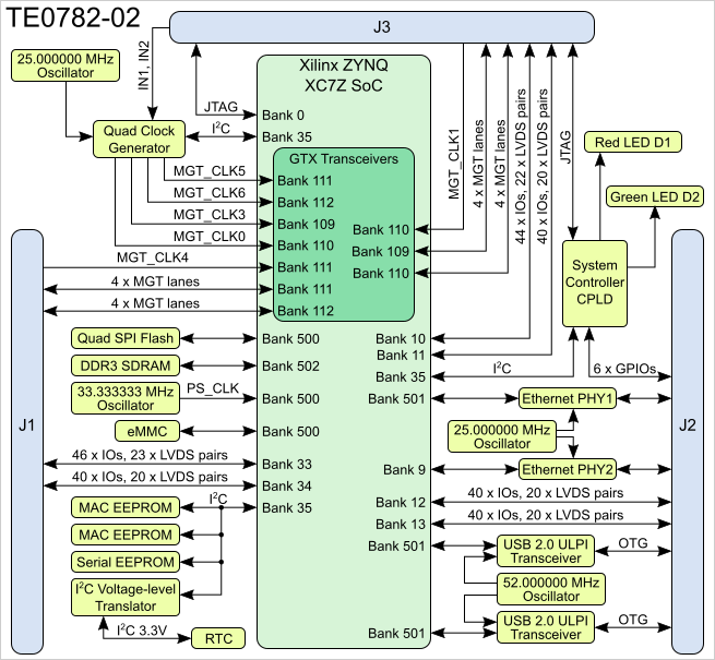
Main Components
- Xilinx Zynq XC7Z SoC (XCZ035, XC7Z045 or XC7Z100), U1
- Lattice Semiconductor MachXO2 1200HC System Controller CPLD, U14
- Intelligent Memory 4Gbit DDR3L-1600 SDRAM, U19
- Intelligent Memory 4Gbit DDR3L-1600 SDRAM, U10
- Spansion 32 MByte QSPI Flash memory, U38
- SI5338A PLL programmable clock generator, U2
- TI low-dropout linear regulator @1.5V, U23
- Microchip USB3320C USB PHY transceiver, U8
- Microchip USB3320C USB PHY transceiver, U4
Intersil ISL12020MIRZ Real Time Clock, U17
- LT quad 4A PowerSoC DC-DC converter (1.0V), U13
LT quad 4A PowerSoC DC-DC converter (3.3V, 1,8V, 1.2V_MGT, 1.0V_MGT), U16
- Samtec ASP-122952-01 160-pin stacking strip (2 rows a 80 positions), J1
- Samtec ASP-122952-01 160-pin stacking strip (2 rows a 80 positions), J2
- Samtec ASP-122952-01 160-pin stacking strip (2 rows a 80 positions), J3
Micron Technology 4 GByte eMMC, U15
- Marvell Alaska 88E1512 Gigabit Ethernet PHY, 20
- Marvell Alaska 88E1512 Gigabit Ethernet PHY, U18
Initial Delivery state
...
24AA025E48 EEPROM's
...
User content not programmed
...
SPI Flash OTP Area
...
Empty, not programmed
...
Except serial number programmed by flash vendor
...
SPI Flash Quad Enable bit
...
Programmed
...
SPI Flash main array
...
demo design
...
eFUSE USER
...
Not programmed
...
...
eFUSE Security
...
Not programmed
...
Signals, Interfaces and Pins
Board to Board (B2B) I/Os
I/O signals connected to the SoC's I/O banks and B2B connector:
...
For detailed information about the pin out, please refer to the Master pin-out table.
JTAG Interface
JTAG access to the Xilinx Zynq device is provided through B2B connector J3.
...
JTAG access to the System Controller CPLD device is provided through B2B connector J3.
...
| Note |
|---|
JTAGENB pin in J3 should be kept low or grounded for normal operation. |
System Controller CPLD I/O Pins
Special purpose pins to configure and operate the System Controller CPLD (IC U14):
...
Some of the functions of the SoM are controlled by the System Controller CPLD and it's firmware. User can change this by using(creating) different firmware for the System Controller CPLD.
On-board LEDs
...
| Page break |
|---|
Clocking
Silicon Labs PLL Si5338 is used to supply reference clock for MGT banks. Optionally MGT reference clocks can also be supplied from the baseboard for any of the MGT banks. Reference clock for the Si5338 quad clock generator itself can be supplied by the on-board oscillator (U3) or from the baseboard.
...
PLL reference
...
25.000000 MHz
...
U3
...
-
...
GT REFCLK1
...
-
...
B2B connector
...
Bank 110, pin AC7/AC8
...
Supplied from baseboard.
...
GT REFCLK4
...
-
...
B2B connector
...
Bank 111, pin U7/U8
...
Supplied from baseboard.
...
Default MIO Mapping
...
Gigabit Ethernet
The TE0782 is equipped with two Marvell Alaska 88E1512 Gigabit Ethernet PHYs (U18 (ETH1) and U20 (ETH2)). The transceiver PHY of ETH1 is connected to the Zynq PS Ethernet GEM0. The I/O Voltage is fixed at 1.8V. The reference clock input for both PHYs is supplied from an on board 25MHz oscillator (U11).
ETH1 PHY connection:
...
Page break
ETH2 PHY connection:
...
-
...
USB Interface
The TE0782 is equipped with two USB PHY's USB3320 from Microchip (U4 (USB0) and U8 (USB1)). The ULPI interface of USB0 is connected to the Zynq PS USB0, ULPI interface of USB1 to Zynq PS USB1. The I/O Voltage is fixed at 1.8V.
The reference clock input of both PHY's is supplied from an on board 52MHz oscillator (U7).
USB0 PHY connection:
...
Page break
USB1 PHY connection:
...
The schematic for the USB connector and required components is different depending on the USB usage. USB standard A or B connectors can be used for Host or Device modes. A Mini USB connector can be used for USB Device mode. A USB Micro connector can be used for Device mode, OTG Mode or Host Mode.
I2C Interface
The on-board I2C components are connected to bank 35 pins L15 (I2C_SDA) and L14 (I2C_SCL).
I2C addresses for on-board components:
...
Pin Definitions
Pins with names ending with _VRN and _VRP are connected to Zynq PL HP bank special purpose pins VRN/VRP and can be routed to DCI calibration resistors on the baseboard. Otherwise they are useable as general purpose I/Os.
Bank 35 has 100 ohm DCI calibration resistors installed, it is also possible to "borrow" the DCI calibration from bank 35 for banks 34 and 33. For more detailed information about the DCI check Xilinx documentation.
On-board peripherals
Processing System (PS) Peripherals
...
optional 2 x 8 MByte HyperRAM (max 2 x 32 MByte HyperRAM)
or optional 2 x 64 MByte HyperFLASH
...
RTC - Real Time Clock
An temperature compensated Intersil ISL12020M is used for Real Time Clock (U17). Battery voltage must be supplied to the module from the baseboard. Battery backed registers can be accessed over I2C bus at slave address 0x6F. General purpose RAM is at I2C slave address 0x57. RTC IC is supported by Linux so it can be used as hwclock device.
| Page break |
|---|
PLL - Phase Locked Loop
The TE0782 is also equipped with a Silicon Labs programmable clock quad generator Si5338A (U2). The Si5338 is accessible for programming over I2C bus at slave address 0x70.
...
Input/Output
...
Default Frequency
...
Notes
...
Externally supplied
...
Needs decoupling on base board
...
IN3
...
25.000000 MHz
...
Fixed input clock
...
CLK0 A/B
...
-
...
GT REFCLK0
...
CLK1 A/B
...
-
...
GT REFCLK3
...
CLK2 A/B
...
GT REFCLK6
...
CLK3 A/B
...
-
...
GT REFCLK5
MAC-Address EEPROM's
Two Microchip 24AA025E48 serial EEPROM's (U22 and U24) are used for storing globally unique 48-bit node addresses, are compatible with EUI-48(TM). The devices are organized as two blocks of 128 x 8-bit memory. One of those blocks stores the 48-bit node address and is write protected, the other block is available for application use. EEPROM's are accessible through I2C nus at slave address 0x50 for MAC-Address1 (U22), 0x51 for MAC-Address2 (U24) .
Boot Process
TE0782's primary boot device is on-board SPI Flash. Boot from on-board eMMC is also supported (FSBL must be loaded from SPI Flash).
JTAG boot mode option is always available.
| Page break |
|---|
Power and Power-On Sequence
Input Power Supply
...
Bank Voltages
...
Power-up sequence at start-up
The Trenz TE0782 SoM is equipped with two quad DC-DC voltage regulators to generate required on-board voltage levels 1V, 3.3V, 1.8V, 1.2V_MGT, 1V_MGT. Additional voltage regulators are used to generate voltages 1.5V, VTT, VTTREF and 1.8V_MGT.
There are following dependencies how the initial voltages of the power rails on the B2B connectors are distributed to the on-board DC-DC converters, which power up further DC-DC converters and the particular on-board voltages:
Power-on sequence is handled by the System Controller CPLD using "Power good"-signals from the voltage regulators:
| Warning |
|---|
| To avoid any damage to the SoM, check on-board voltages in steady state before applying VCCIO voltages to the SoC's I/O banks. |
Voltage levels of the I/O signals must not get higher than VCCIO + 0.4V.Board to Board Connectors
The TE0782 module has three 160-pin double-row ASP-122952-01 Samtec connectors on the bottom side which mate with ASP-122953-01 Samtec connectors on the baseboard. Mating height is 5 mm.
Variants Currently In Production
...
SoC Junction Temperature
...
Technical Specification
Absolute Maximum Ratings
...
VIN supply voltage
...
-0.3
...
15
...
V
...
VIN33 supply voltage
...
-0.5
...
3.75
...
V
...
Voltage on module JTAG pins
...
-0.4
...
V
...
Storage temperature
...
-40
...
+85
...
C
...
| Note |
|---|
| Assembly variants for higher storage temperature range on request |
Recommended Operating Conditions
...
| Note |
|---|
| Please check Xilinx Datasheet for complete list of Absolute maximum and recommended operating ratings for the Zynq device (DS181 Artix or DS182 Kintex). |
| Page break |
|---|
Operating Temperature Ranges
Industrial grade: -40°C to +85°C.
Module operating temperature range depends on customer design and cooling solution. Please contact us for options.
Physical Dimensions
Please download the assembly diagram for exact values.
Module size: 85 mm × 85 mm.
Mating height with standard connectors: 5 mm
PCB thickness: 1,7 mm
All dimensions are shown in millimeters.
Weight
...
Weight
...
Part
...
60 g
...
Plain module
Revision History
Hardware Revision History
...
02
...
First production release
...
Hardware revision number is printed on the PCB board together with the module model number separated by the dash.
Document Change History
| Date | Revision | Contributors | Description | 2017-06-07 | Jan Kumann | Minor formatting |
|---|---|---|---|
| 2017-05-23 | V13
| Jan Kumann | New block diagram. New product images. New physical dimensions drawing. |
| 2017-01-24 | V12
| Ali Naseri | New numbered pictures describing main components. Added variants in production. |
| 2016-06-27 | v10 | Ali Naseri, Jan Kumann | Initial release.
Disclaimer
| Include Page | ||||
|---|---|---|---|---|
|
Overview
Content Tools