Page History
...
| Scroll Only (inline) |
|---|
On https://wiki.trenz-electronic.de/display/PD/TE0782-02+TRM the online version of this manual and other documents can be found. |
The Trenz Electronic TE0782 is a high-performance, industrial-grade SoM (System on Module) with industrial temperature range based on Xilinx Zynq-7000 SoC. It is equipped with a Xilinx Zynq-7 (XC7Z035, XC7Z045 or XC7Z100).
...
- 2 x Gbps Ethernet PHY transceiver
- 32-Bit DDR3 SDRAM 1Gbyte
- 32 MByte QSPI Flash Memory for configuration, operation and to store data
- eMMC (4 GByte in standard configuration)
- 2 x USB PHY transceiver
- 16 GTX high-performance transceiver lanes
- powerful switch-mode power supplies for all on-board voltages
- large number of configurable I/Os is provided via rugged high-speed stacking strips
Block
...
Diagram
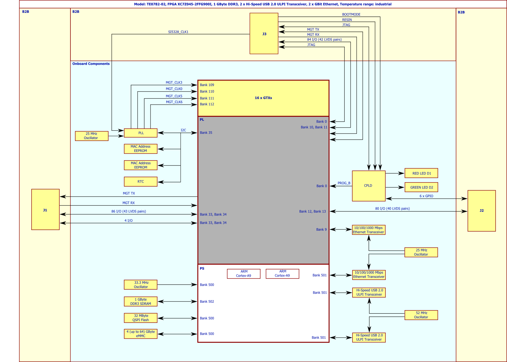
Key Features
- Xilinx Zynq-7 XC7Z035, XC7Z045 or XC7Z100 SoM
- Rugged for shock and high vibration
- Dual ARM Cortex-A9 MPCore
- 1 GByte DDR3 SDRAM (2 x 16RAM (32-Bit wide 512 MByte DDR3 SDRAM)
- 32 MByte QSPI Flash memory
- 2 x Hi-Speed USB2.0 ULPI transceiver PHY
- 2 x Gigabit (10/100/1000 Mbps) Ethernet transceiver PHY
- 4 GByte eMMC (optional up to 64GByte)
- 2 x MAC-Address EEPROMs
- optional 2 x 8 MByte HyperRAM (max 2 x 32 MByte HyperRAM) or optional 2 x 64 MByte HyperFLASH
- Temperature compensated RTC (real-time clock)
- Si5338 PLL for GTX Transceiver clocks
- Plug-on module with 3 x 160-pin high-speed strips
- 16 GTX high-performance transceiver lanes
- GT transceiver clock inputs
- 254 FPGA I/O's (125 LVDS pairs)
- On-board high-efficiency DC-DC converters
- System management
- eFUSE bit-stream encryption
- AES bit-stream encryption
- Evenly-spread supply pins for good signal integrity
- User LED
...
| Name | Note |
|---|---|
| BOOTMODE | user configurable (CPLD) |
| CONFIGX | user configurable (CPLD) |
| JTAGENBJTAG operation | special mode pin for SC CPLD |
| RESIN | System-reset |
| CLPD_GPIO0user GPIO | Function defined by CPLD Firmware |
| CLPD_GPIO1user GPIO | Function defined by CPLD Firmware |
| CLPD_GPIO2user GPIO | Function defined by CPLD Firmware |
| CLPD_GPIO3user GPIO | Function defined by CPLD Firmware |
| CLPD_GPIO4user GPIO | Function defined by CPLD Firmware |
| CLPD_GPIO5 | Function defined by CPLD Firmware |
| CLPD_GPIO6 | |
| CLPD_GPIO7 | user GPIO |
Small CPLD controls some functions of the SoM, this CPLD can be updated by the end user if support is designed in on customer base.
Boot Modes
...
Silabs Multisynth PLL Si5338 can deliver GT reference clocks to all 4 GT Banks. Additionally a GT Reference clock can be generated on the base board for any of the 4 GT Banks. There is reference clock available on the TE0782 for Si5338, there is no need to supply a master optionally external reference clock can be supplied from the base.
| Clock | Frequency | IC | ZYNQ PS / PL | Notes | ||
|---|---|---|---|---|---|---|
| PS CLK | 33.3333 MHz | U61 | BANK500, PS _ CLK | PS Subsystem main clock | ||
| 10/100/1000 Mbps ETH PHYs reference | 25 MHz | U11 | - | |||
| USB PHY reference | 52 MHz | U7 | - | |||
PLL reference | 25 MHz | U3 | - | |||
GT REFCLK1 | - | B2B connector | BANK110, Pin AC7/AC8 | Externally supplied from base | ||
GT REFCLK4 | - | B2B connector | BANK111, Pin U7/U8 | Externally supplied from base | ||
| Si5338 CLK0 | quad programmable clock (I2C) SI5338A | user | U2 | BANK110, Pin AA8/AA7 | ? | |
| Si5338 CLK1 | U2 | BANK109, Pin AF10/AF9 | ? | |||
| Si5338 CLK2 | U2 | BANK111, Pin W8/W7 | ? | |||
| Si5338 CLK3 | U2 | BANK112, Pin N8/N7 | GT REFCLK0 GT REFCLK3 GT REFCLK5 GT REFCLK6 | ? |
Processing System (PS) Peripherals
| Peripheral | IC | Designator | ZYNQ PS / PL | MIO | Notes |
|---|---|---|---|---|---|
| QSPI Flash | S25FL256SAGBHI20 | U38 | PS QSPI0 | MIO1...MIO6 | - |
| ETH0 10/100/1000 Mbps PHY | 88E1512-A0-NNP2I000 | U18 | PS ETH0; GPIO BANK35 | MIO16...MIO27, MIO52, MIO53 | - |
| ETH0 10/100/1000 Mbps PHY Reset | PS GPIO | MIO7 | ETH1_RESET33 (MIO7) -> CPLD -> ETH1_RESET | ||
| ETH1 10/100/1000 Mbps PHY | 88E1512-A0-NNP2I000 | U20 | GPIO BANK9, BANK35 | - | PHY can be used with soft Ethernet MAC IP also |
| ETH1 10/100/1000 Mbps PHY Reset | GPIO BANK35, Pin B15 | - | - | ||
| USB0 | USB3320C-EZK | U4 | PS USB0 | MIO28...MIO39 | - |
| USB0 Reset | PS GPIO | MIO0 | OTG_RESET33 (MIO0) -> CPLD -> OTG_RESET | ||
| USB1 | USB3320C-EZK | U8 | USB1 | MIO40...MIO51 | - |
| USB1 Reset | PS GPIO | MIO0 | OTG_RESET33 (MIO0) -> CPLD -> OTG_RESET | ||
| Clock PLL | Si5338 | U2I2C | BANK35, Pin L14/L15 | Low jitter phase locked loop | |
| e-MMC (embedded e-MMC) | MTFC4GMVEA-4M IT | U15 | SDIO0 | MIO10...MIO15 | - |
| HyperFlash RAM | S26KS512SDPBHI00x | U9 | GPIO BANK35 | - | optional 2 x 8 MByte HyperRAM (max 2 x 32 MByte HyperRAM) or optional 2 x 64 MByte HyperFLASH |
| HyperFlash RAM | S26KS512SDPBHI00x | U12 | GPIO BANK35 | - | as above |
| EEPROM I2C | 24LC128-I/ST | U26 | GPIO BANK35, Pin L14/L15 | - | - |
| EEPROM I2C | 24AA025E48T-I/OT | U22 | GPIO BANK35, Pin L14/L15 | - | MAC Address |
| EEPROM I2C | 24AA025E48T-I/OT | U24 | GPIO BANK35, Pin L14/L15 | - | MAC Address |
| RTC | ISL12020MIRZ | U17 | GPIO BANK35, Pin L14/L15 | - | Temperature compensated real time clock |
| RTC Interrupt | ISL12020MIRZ | U17 | - | - | RTC_INT -> CPLD |
...
| MIO | Configured as | B2B | Notes |
|---|---|---|---|
| 0OTG | -RST33USB Reset | - | connected to CPLD used as level translator |
| 1 | QSPI0 | - | SPI Flash-CS |
| 2 | QSPI0 | - | SPI Flash-DQ0 |
| 3 | QSPI0 | - | SPI Flash-DQ1 |
| 4 | QSPI0 | - | SPI Flash-DQ2 |
| 5 | QSPI0 | - | SPI Flash-DQ3 |
| 6 | QSPI0 | - | SPI Flash-SCK |
| 7ETH1 | _RESET33Ethernet Reset | - | connected to CPLD used level translator |
| 8, | GPIOUART | -connected to CPLD and Pull-Up 3.3V | |
| 9 | GPIOUART | - | connected to CPLD |
| 10 | MMC-SDIO1 D0 | - | - |
| 11 | MMC-SDIO1 CMD | - | - |
| 12MMC-CCLK | SDIO1 CLK | - | - |
| 13 | MMC-SDIO1 D1 | - | - |
| 14 | MMC-SDIO1 D2 | - | - |
| 15 | MMC-SDIO1 D3 | - | - |
| 16..27 | ETH0 | - | Ethernet RGMII PHY |
| 28..39 | USB0 | - | USB0 ULPI PHY |
| 40...51 | USB1 | - | USB1 ULPI PHY |
| 52 | ETH0 MDC | - | - |
| 53 | ETH0 MDIO | - | - |
...
| Device | IC | Designator | I2C-Address | Notes |
|---|---|---|---|---|
| EEPROM | 24LC128-I/ST | U26 | 0x53 | user data, parameter |
| EEPROM | 24AA025E48T-I/OT | U22 | 0x50 | MAC Address/EEPROM |
| EEPROM | 24AA025E48T-I/OT | U24 | 0x51 | MAC Address/EEPROM |
| RTC | ISL12020MIRZ | U17 | 0x6F | Temperature compensated real time clock |
| Battery backed RAM | ISL12020MIRZ | U17 | 0x57 | integrated in RTC |
| PLL | SI5338A-B-GMR | U2 | 0x70 | Quad reference clock for GTX transceiver lanes |
| CPLD | LCMXO2-1200HC-4TG100I | U14 | user | - |
...
Number of I/O's connected to the SoC's I/O bank and B2B connector
| Bank | Type | VCCIO Max | B2BConnector | IO count | Differentíal | IO Voltage | Notes | ||
|---|---|---|---|---|---|---|---|---|---|
| 10 | HR | 3.3V | J3 | 44 | 22 | user | 22 LVDS-pairs possible | ||
| 11 | HR | 3.3V | J3 | 40 | 20 | user | 20 LVDS-pairs possible | ||
| 12 | HR | 3.3V | J2 | 40 | 20 | user | 20 LVDS-pairs possible | ||
| 13 | HR | 3.3V | J2 | 40 | 20 | user | 20 LVDS-pairs possible | ||
| 33HR | HP | 1.8V | J1 | 48 | 23 | user | 23 LVDS-pairs possible | ||
| 34 | HR | HP | 1.8V | J1 | 42 | 20 | user | 20 LVDS-pairs possible |
For detailed information about the pin out, please refer to the Master Pinout Table.
...
| Frequency of LED-Toggling [1/2.6sec] | Status |
|---|---|
| 1 | Power problem |
| 2 | MGT Power problem |
| 3 | Reset from mainboardbase board |
| 4 | FPGA not programmed |
This function depend on the CPLD revision.
D2 - On- Onboard board GREEN LED
Green LED connected to MIO8
...
| PHY PIN | ZYNQ PS / PL | System Controller CPLD | Notes |
|---|---|---|---|
| MDC/MDIO | BANK35, Pin C17/B17 | - | - |
| LED0 | BANK35, Pin K15 | - | - |
| LED1 | BANK35, Pin B16 | - | - |
| Interrupt | BANK35, Pin A17 | - | - |
| CONFIG | BANK35, Pin E15 | - | Pin connected to GND, PHY Address is strapped to 0x00 by default |
| RESETn | BANK35, Pin B15 | - | - |
| RGMII | BANK9 | - | - |
| MDI | - | - | on B2B J2 connector- |
USB
The TE0782 is equipped with two USB PHYs USB3320 from Microchip (U4 (USB0) and U8 (USB1)). The ULPI interface of USB0 is connected to the Zynq PS USB0, ULPI interface of USB1 to Zynq PS USB1. The I/O Voltage is fixed at 1.8V.
...
Input/Output | Default Frequency | Notes | |||
|---|---|---|---|---|---|
| IN1/IN2 | Externally supplied | need decoupling on base board | |||
IN3 | 25MHz | Fixed input clock | IN5 | - | not available and not used|
IN4/IN6 | - | connected to Ground | |||
CLK0 A/B | - | GT REFCLK0 | |||
CLK1 A/B | - | GT REFCLK3 | |||
CLK2 A/B | - | GT REFCLK6 | |||
CLK3 A/B | - | GT REFCLK5 |
...
| Bank | Voltage | max. Value | note |
|---|---|---|---|
| 0 | 3,.3 V | - | FPGA Configuration |
| 502 | 1,.5 V | - | DDR3-RAM Port |
| 109 / 110 / 111 / 112 | 1,.2 V | - | FPGA MGT |
| 500 / 501 | 3,.3 V | - | MIO Banks |
| 9 | 1,.8 V | - | ETH2 RGMII |
| 10 | user | 3,.3 V | B2B name: VCCIO_10 |
| 11 | user | 3,.3 V | B2B name: VCCIO_11 |
| 12 | user | 3,.3 V | B2B name: VCCIO_12 |
| 13 | user | 3,.3 V | B2B name: VCCIO_13 |
| 33 | user | 3,3 1.8 V | B2B name: VCCIO_33 |
| 34 | user | 3,3 1.8 V | B2B name: VCCIO_34 |
| 35 | 1,.8 V | - | Hyper-RAM, Ethernet, I2C |
...
| Parameter | Min | Max | Units | Notes |
|---|---|---|---|---|
Vin supply voltage | -0.36.0 |
| V | |
Vin33 supply voltage | -0.43.6 |
| V | |
| VBat supply voltage | -1 | 6.0 | V | |
| PL IO Bank supply voltage for HR I/O banks (VCCO) | -0.5 | 3.6 | V | |
| I/O input voltage for HP I/O banks | -0.55 | VCCO_X+0.55 | V | TE0782 does not have HP banks |
Voltage on Module JTAG pins | -0.4 | VCCO_0+0.55 | V | VCCO_0 is 3.3V nominal |
Storage Temperature | -40 | +85 | C | |
| Storage Temperature without the ISL12020MIRZ | -55 | +100 | C |
...
| Parameter | Min | Max | Units | Notes | Reference document | |
|---|---|---|---|---|---|---|
| Vin supply voltage | 2.5 | 5.5 | V | |||
| Vin33 supply voltage | 3.135 | 3.465 | V | |||
| VBat supply voltage | 2.7 | 5.5 | V | |||
| PL IO Bank supply voltage for HR I/O banks (VCCO) | 1.14 | 3.465 | V | Xilinx document DS191 | ||
| I/O input voltage for HR I/O banks | (*) | (*) | V | (*) Check datasheet | Xilinx document DS191 and DS187 | |
| Voltage on Module JTAG pins | 3.135 | 3.465 | V | VCCO_0 is 3.3 V nominal |
...
All dimensions are shown in mm.
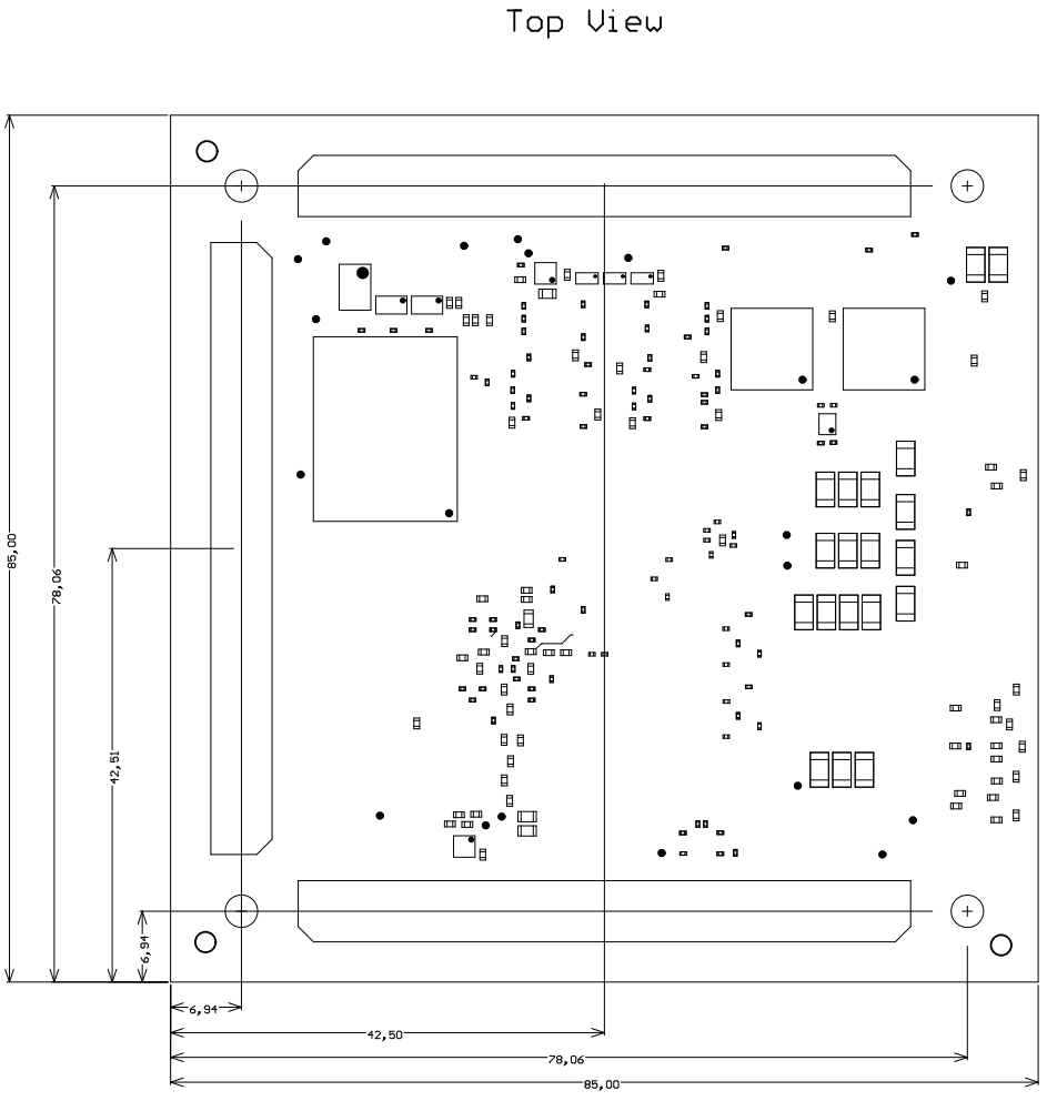
WeigtWeight | Part |
|---|---|
60 g | Plain module |
Temperature Ranges
...
Overview
Content Tools