| Page properties |
|---|
|
Template Revision 2.2
TRM Name always "TE Series Name" +TRM, for example "TE0720 TRM" |
| HTML |
|---|
<!-- tables have all same width (web max 1200px and pdf full page(640px), flexible width or fix width on menu for single column can be used as before) -->
<style>
.wrapped{
  width: 100% !important;
  max-width: 1200px !important;
 }
</style> |
| Page properties |
|---|
|
Important General Note:
|
| Page properties |
|---|
|
----------------------------------------------------------------------- |
| Page properties |
|---|
|
Note for Download Link of the Scroll ignore macro: |
| Scroll pdf ignore |
|---|
Table of Contents |
Overview
The Trenz Electronic TE0701 Carrier Board is a baseboard for 4 x 5 SoMs, which exposes the module's B2B connector pins to accessible connectors and provides a whole range of on-board components to test and evaluate TE 4 x 5 SoMs.
See page "4 x 5 cm carriers" to get information about the SoMs supported by the TE0701 carrier board.
Refer to http://trenz.org/te0701-info for the current online version of this manual and other available documentation.
Key Features
| Page properties |
|---|
|
Notes: - List of key features of the PCB
|
- Barrel jack for 12V power supply
- Overvoltage-, undervoltage- and reversed- supply-voltage-protection
- System Controller CPLD Lattice MachXO2 1200HC
- ARM JTAG interface connector
- Mini Camera Link
- RJ45 Gigabit Ethernet MagJack
- Low pin count FPGA Mezzanine Card (FMC LPC) connector
- USB JTAG and UART interface (FTDI FT2232HQ) with Mini-USB connector
- ADV7511 HDMI transmitter with HDMI connector
- 8 x red user LEDs
- 2 x user push-button
- 2 x 4-bit DIP switch for baseboard configuration
- Pmod connectors
- Micro SD card socket
- Micro-USB interface (device, host or OTG modes)
Trenz Electronic 4 x 5 modules high-speed connector strips (3x Samtec LSHM series connectors)
Block Diagram
| Scroll Title |
|---|
| anchor | Figure_OV_BD |
|---|
| title | TE0701-06 block diagram |
|---|
|
| Scroll Ignore |
|---|
| draw.io Diagram |
|---|
| border | false |
|---|
| viewerToolbar | true |
|---|
| |
|---|
| fitWindow | false |
|---|
| diagramName | TE0701 block diagram |
|---|
| simpleViewer | false |
|---|
| links | auto |
|---|
| tbstyle | hidden |
|---|
| lbox | true |
|---|
| diagramWidth | 641 |
|---|
|
|
| Scroll Only |
|---|
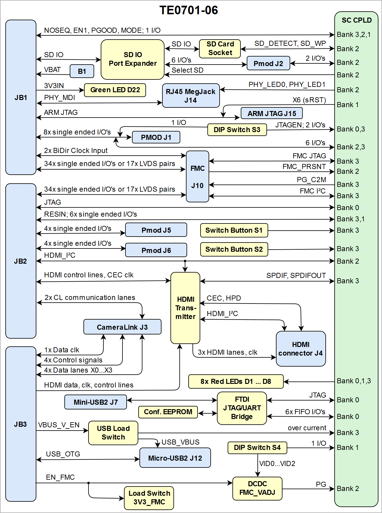 Image Added Image Added
|
|
Main Components
| Page properties |
|---|
|
Notes : - Picture of the PCB (top and bottom side) with labels of important components
- Add List below
|
| Scroll Title |
|---|
| anchor | Figure_OV_MC |
|---|
| title | TE0701-06 main components |
|---|
|
| Scroll Ignore |
|---|
| draw.io Diagram |
|---|
| border | false |
|---|
| viewerToolbar | true |
|---|
| |
|---|
| fitWindow | false |
|---|
| diagramName | TE0701 main components |
|---|
| simpleViewer | false |
|---|
| links | auto |
|---|
| tbstyle | hidden |
|---|
| lbox | true |
|---|
| diagramWidth | 641 |
|---|
| revision | 1 |
|---|
|
|
| Scroll Only |
|---|
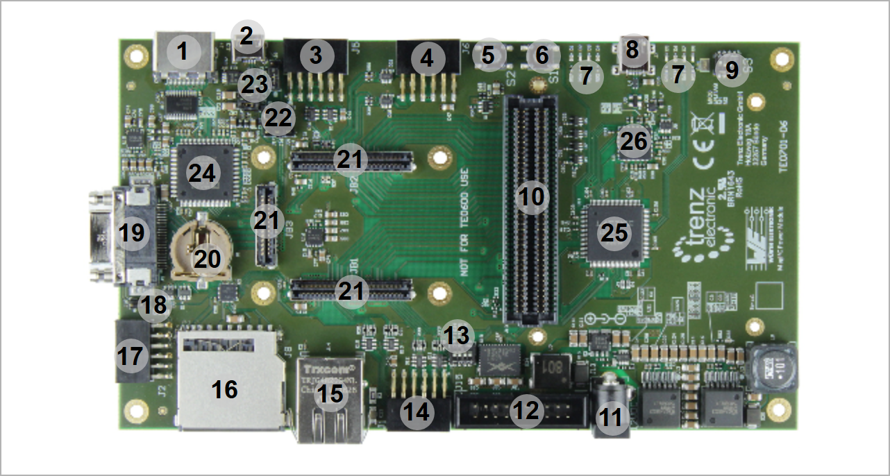 Image Added Image Added
|
|
- HDMI connector (1.4 HEAC support), J4
- Micro-USB2 connector, J12
Pmod connector, J5
- Pmod connector, J6
- User push-button ("RESTART" button by default), S2
- User push-button ("RESET" button by default), S1
- 8x red user LEDs, D1 ... D8
- Mini-USB2 connector, J7
- User 4-bit DIP switch, S3
- VITA 57.1 compliant LPC FMC connector, J10
- Barrel jack for 12V power supply, J13
- ARM JTAG connector (DS-5 D-Stream), J15, functionality depends on module
- User 4-bit DIP switch, S4
- Pmod connector, J1
- RJ45 Gigabit Ethernet connector, J14
- SD Card connector, J8
- Pmod connector, J2
- Jumper, J18
- Mini CameraLink connector, J3
- CR1220 Backup-Battery holder, B1
- Trenz Electronic 4 x 5 modules B2B connectors, JB1 ... JB3
- Jumper J16, J17, J21
- Jumper J9, J19, J20
- Analog Devices ADV7511 HDMI Transmitter, U1
- Lattice Semiconductor MachXO2 1200 HC System Controller CPLD, U14
- FTDI FT2232H USB2 to JTAG/UART Bridge, U3
Initial Delivery State
| Scroll Title |
|---|
| anchor | Table_OV_IDS |
|---|
| title | Initial delivery state of programmable devices on the board |
|---|
|
| Scroll Table Layout |
|---|
| orientation | portrait |
|---|
| sortDirection | ASC |
|---|
| repeatTableHeaders | default |
|---|
| sortByColumn | 1 |
|---|
| sortEnabled | false |
|---|
| cellHighlighting | true |
|---|
|
Storage device name | Content | Notes |
|---|
FTDI chip configuration EEPROM U9 (ST M93C66) | Xilinx License | Do not overwrite, see warning in related section | | System Controller CPLD U14 | SC CPLD Firmware | - |
|
Control Signals
To get started with TE0701 board, some basic control signals are essential and are described in the following table:
| Scroll Title |
|---|
| anchor | Table_OV_CS |
|---|
| title | TE0701 Control Signals |
|---|
|
| Scroll Table Layout |
|---|
| orientation | portrait |
|---|
| sortDirection | ASC |
|---|
| repeatTableHeaders | default |
|---|
| sortByColumn | 1 |
|---|
| sortEnabled | false |
|---|
| cellHighlighting | true |
|---|
|
Control signal | Switch / Button / LED / Pin | Signal Schematic Names | Connected to | Functionality | Notes |
|---|
| SC CPLD JTAG Enable | DIP switch S3-3 | JTAGEN | SC CPLD U14, pin 82 | ON: FPGA JTAG enabled
OFF:SC CPLD JTAG enabled, | - | | BOOT MODE | SC CPLD U14, pin 27 | MODE | B2B JB1, pin 31 | Boot Mode for attached module (Flash or SD) | - | | Module Reset | SC CPLD U14, pin 13 | RESIN | B2B JB2, pin 17 | Module Reset | - | | Global Reset input | Push Button S2 | S2 | SC CPLD U14, pin 2 | Manual reset from user | - | | SD Card detection | SD Slot J8, pin 10 | SD_DETECT | SC CPLD U14, pin 40 | Detection Signal for inserted SD Card | Boot mode is set to SD Boot,
when SD Card is detected. | | Board status indicators | Red LEDs D1 ... D8 | ULED1 ... ULED8 | SC CPLD U14, pins
78, 77, 76, 16, 69, 68, 65, 64 | indicating various board and
module status / configuration | Refer to the firmware documentation of the SC CPLD
U14 and to the subsection 'LEDs' in section 'On-board Peripherals'
for more details and current functionality. | | Board 3.3V power indicator | Green LED D22 | 3V3IN | B2B JB1, pin 14, 16 | ON: 3.3V on-board voltage available | - | | FMC_VADJ voltage selection | DIP switches S4-1, S4-2, S4-3 | VID0 ... VID2 | SC CPLD U14, pins 34, 35, 38 | sets adjustable voltage for FMC connector | - | | I²C control / FMC_VADJ voltage selection | DIP switches S3-2, S3-1 | CM0, CM1 | SC CPLD U14, pins 99, 1 | enabling / disabling I²C control of board functionalities,
sets FMC_VADJ voltage (only 3 steps),
available to user if FMC_VADJ set by DIP-switch S4 | Refer to the firmware documentation of the SC CPLD
U14 and and to the subsection 'DIP switches' in section 'On-board
Peripherals' for current functionality and more details. |
|
Signals, Interfaces and Pins
| Page properties |
|---|
|
Notes: - For carrier or stand-alone boards use subsection for every connector typ (add designator on description, not on the subsection title), for example:
- For modules which needs carrier us only classes and refer to B2B connector if more than one is used, for example
|
FMC LPC Connector
I/O signals and interfaces connected to the FPGA SoCs I/O bank and FMC connector J10:
| Scroll Title |
|---|
| anchor | Table_SIP_FMC |
|---|
| title | FMC connector J10 interface |
|---|
|
| Scroll Table Layout |
|---|
| orientation | portrait |
|---|
| sortDirection | ASC |
|---|
| repeatTableHeaders | default |
|---|
| sortByColumn | 1 |
|---|
| sortEnabled | false |
|---|
| cellHighlighting | true |
|---|
|
| FMC Connector J2 Pins and Interfaces | I/O Signal Count | LVDS-pairs count | Connected to | VCCIO voltage | Notes |
|---|
| I/O | 34 | 17 | B2B JB1 connector | FMC_VADJ / 3V3_FMC | pins usable as single ended I/O's and LVDS pairs | | 34 | 17 | B2B JB2 connector | FMC_VADJ / 3V3_FMC | | I²C | 2 | - | SC CPLD U14, pin 8, 10 | - | FMC I²C Geographical Address pins GA0 and GA1 set to GND. | | JTAG | 4 | - | SC CPLD U14, pin 4, 7, 9, 12 | 3.3V | - | | Clock Input | - | 2 | B2B JB1 connector | - | 2x bidirectional reference clock inputs | | Control Signals | 2 | - | SC CPLD U14, pin 20, 28 | - | 'PG_C2M', 'FMC_PRSNT' | | Reference voltage (FMC_VREF) | 1 | - | B2B JB1 connector, pin 85, 97
B2B JB2 connector, pin 37, 93 | - | FMC sets thresholds of attached module's reference voltage (VREF pins). |
|
ARM JTAG Connector
The TE0701 baseboard offers the ARM JTAG 20-pin connector (2.54mm pitch). It can be used in standard JTAG or Serial Wire Debug (SWD) mode.
The following table contains the ARM JTAG connector pinout:
| Scroll Title |
|---|
| anchor | Table_SIP_ARM_JTAG |
|---|
| title | ARM JTAG connector signals and pins |
|---|
|
| Scroll Table Layout |
|---|
| orientation | portrait |
|---|
| sortDirection | ASC |
|---|
| repeatTableHeaders | default |
|---|
| sortByColumn | 1 |
|---|
| sortEnabled | false |
|---|
| cellHighlighting | true |
|---|
|
Connector J15 pin
| Schematic Name | Connected to | Notes |
|---|
1, VTREF | FMC_VADJ | DCDC U18 | Voltage Target Reference | | 2, not connected | - | - | - | | 3, NTRST | X0 | B2B JB1, pin 32 | active low Test Reset | 4, GND | - | - | - | | 5, TDI | X1 | B2B JB1, pin 34 | Test Data In | | 6, GND | - | - | - | | 7, TMS / SWDIO | X2 | B2B JB1, pin 36 | Test Mode Select | | 8, GND | - | - | - | | 9, TCK / SWCLK | X3 | B2B JB1, pin 38 | Test Clock | | 10, GND | - | - | - | 11, RTCK | X4 | B2B JB1, pin 42 | Return Test Clock | | 12, GND | - | - | - | | 13, TDO / SWO | X5 | B2B JB1, pin 44 | Test Data Out | | 14, not connected | - | - | - | | 15, sRST | X6 | B2B JB1, pin 99 | active low System Test Reset | | 16, not connected | - | - | - | | 17, not connected | - | - | - | | 18, GND | - | - | - | | 19, not connected | - | - | - | | 20, GND | - | - | - |
|
Mini-USB2 B Connector
Mini-USB2 interface provides access to UART and JTAG functions via FTDI FT2232 chip. The signals are forwarded to the B2B connectors via SC CPLD U14. 4 additional I/O's connected to the SC CPLD are available to the user.
JTAG access to the System Controller CPLD and attached module is provided via mini-USB JTAG interface J7 (FTDI FT2232H) and controlled by DIP switch S3-3.
The JTAG port of the System Controller CPLD is enabled by setting switch S3-3 JTAGEN to the OFF position.
| Scroll Title |
|---|
| anchor | Figure_SIP_JTAG/UART |
|---|
| title | JTAG/UART interface |
|---|
|
| Scroll Ignore |
|---|
| draw.io Diagram |
|---|
| border | false |
|---|
| viewerToolbar | true |
|---|
| |
|---|
| fitWindow | false |
|---|
| diagramName | TE0701 MiniUSB2 interface |
|---|
| simpleViewer | false |
|---|
| links | auto |
|---|
| tbstyle | hidden |
|---|
| lbox | true |
|---|
| diagramWidth | 641 |
|---|
| revision | 1 |
|---|
|
|
| Scroll Only |
|---|
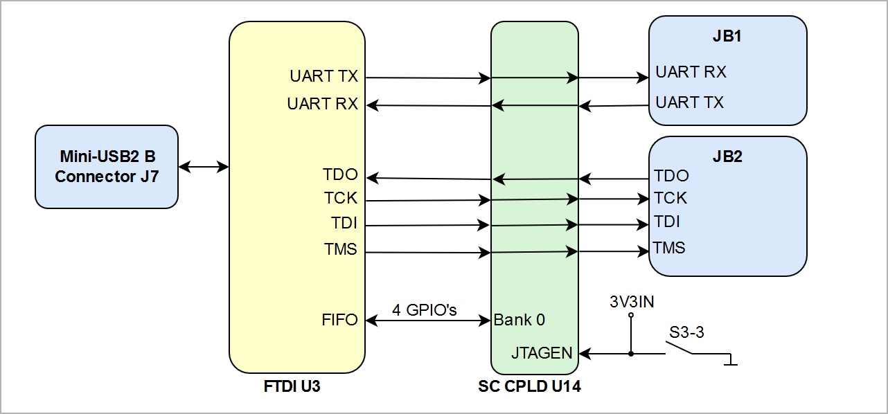 Image Added Image Added
|
|
Micro-USB2 Connector
The TE0701 carrier board can be configured as a USB host. Hence, it must provide from 5.25V to 4.75V to the board side of the downstream connection (micro-USB port on J12). To provide sufficient power, a TPS2051 power distribution switch is located on the carrier board in between the 5V power supply and the VBUS signal of the USB downstream port interface. If the output load exceeds the current-limit threshold, the TPS2051 limits the output current and pulls the over-current logic output (OC_n) low, which is routed to the on-board CPLD. The TPS2051 is put into operation by setting J19 CLOSED. J20 provides an extra 200µF decoupling capacitor (in addition to 10µF) to further stabilize the output signal. Moreover, a series terminating resistor of either 10K (J9: 1-2, 3) or 1K (J9: 1, 2-3) is selectable on the "USB-VBUS" signal. Both signals, USB-VBUS and VBUS_V_EN (that enables the TPS2051 on "high") are routed (as well as the corresponding D+/- data lines) via the on-board connector directly to the USB 2.0 high-speed transceiver PHY of the mounted SoM. In summary, the default jumper settings are the following: J9: 1-2, 3 (10K series terminating resistor); J19: CLOSED (TPS2051 in operation); J20: CLOSED (200 µF added).
| Scroll Title |
|---|
| anchor | Figure_SIP_MicroUSB2 |
|---|
| title | TE0701 MicroUSB2 interface configuration |
|---|
|
| Scroll Ignore |
|---|
| draw.io Diagram |
|---|
| border | false |
|---|
| viewerToolbar | true |
|---|
| |
|---|
| fitWindow | false |
|---|
| diagramName | TE0701 MicroUSB2 interface |
|---|
| simpleViewer | false |
|---|
| links | auto |
|---|
| tbstyle | hidden |
|---|
| lbox | true |
|---|
| diagramWidth | 641 |
|---|
| revision | 1 |
|---|
|
|
| Scroll Only |
|---|
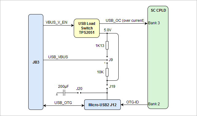 Image Added Image Added
|
|
MMC/SD-Card Socket
MMC/SD-Card socket is not directly wired to the B2B connector pins, but through a Texas Instruments TXS02612 SDIO Port Expander, which is needed for voltage translation due to different voltage levels of the Micro SD Card and MIO-bank of the Xilinx Zynq module. The Micro SD Card has 3.3V signal voltage level, but the MIO-bank on the Xilinx Zynq module has VCCIO of 1.8V.
With SD_SEL signal connected to the Texas Instruments TXS02612 SDIO Port Expander user can choose which port is accessible. Port B0 of SDIO Port Expander is connected to the Micro SD Card connector and B1 is connected to the Pmod J2 connector. SEL_SD signal can be controlled by the System Controller CPLD firmware.
| Scroll Title |
|---|
| anchor | Table_SIP_SD/MMC |
|---|
| title | SD/MMC Card socket signals and pins |
|---|
|
| Scroll Table Layout |
|---|
| orientation | portrait |
|---|
| sortDirection | ASC |
|---|
| repeatTableHeaders | default |
|---|
| sortByColumn | 1 |
|---|
| sortEnabled | false |
|---|
| cellHighlighting | true |
|---|
|
| Connector J8 pin | Signal Schematic Name | Muxed to signal on Port Expander | Connected to | Notes |
|---|
| 1, DAT3 | DAT3/CS | SD_DAT3 | B2B JB1, pin 18 | - | 2, CMD | CMD/MOSI | SD_CMD | B2B JB1, pin 26 | - | 5, CLK | S_CLK | SD_CLK | B2B JB1, pin 28 | - | 7, DAT0 | DAT0/MISO | SD_DAT0 | B2B JB1, pin 24 | - | 8, DAT1 | DAT1 | SD_DAT1 | B2B JB1, pin 22 | - | 9, DAT2 | DAT2 | SD_DAT2 | B2B JB1, pin 20 | - | 10, CD | SD_DETECT | - | SC CPLD U14, pin 40 | Card Detect | 11, WP | SD_WP | - | SC CPLD U14, pin 41 | Write Protect |
|
RJ45 - Ethernet
The TE0701 Carrier Board has a RJ45 Gigabit Ethernet MagJack (J14) with two LEDs. On-board Ethernet MagJack J14 pins are routed to B2B connector JB1 via MDI. The center tap of the magnetics is not connected to module's B2B connector. PHY LEDs are not connected directly to the module's B2B connectors as the 4 x 5 module have no dedicated PHY LED pins assigned. PHY LEDs are connected to the TE0701 System Controller CPLD and can be routed to some of the module's I/O pins with firmware.
See documentation of the TE0701 System Controller CPLD to get information of the function of the PHY LEDs.
| Scroll Title |
|---|
| anchor | Table_SIP_RJ45 |
|---|
| title | RJ45 Ethernet MagJack signals and pins |
|---|
|
| Scroll Table Layout |
|---|
| orientation | portrait |
|---|
| sortDirection | ASC |
|---|
| repeatTableHeaders | default |
|---|
| sortByColumn | 1 |
|---|
| sortEnabled | false |
|---|
| cellHighlighting | true |
|---|
|
| RJ45 MagJack J14 pin | Signal Schematic Name | Connected to | Notes |
|---|
| LED1 | PHY_LED1 | SC CPLD U14, pin 42 | Yellow | | LED2 | PHY_LED2 | SC CPLD U14, pin 43 | Green | | PHY_MDI | PHY_MDI0_P | B2B JB1, pin 3 | - | | PHY_MDI0_N | B2B JB1, pin 5 | - | | PHY_MDI1_P | B2B JB1, pin 9 | - | | PHY_MDI1_N | B2B JB1, pin 11 | - | | PHY_MDI2_P | B2B JB1, pin 15 | - | | PHY_MDI2_N | B2B JB1, pin 17 | - | | PHY_MDI3_P | B2B JB1, pin 21 | - | | PHY_MDI3_N | B2B JB1, pin 23 | - |
|
Mini CameraLink Connector
The TE0701 board provides the high speed CameraLink interface for visual input. The CameraLink is connected with 11 LVDS-pairs to the B2B connectors JB2 and JB3 which create data receive and control lanes.
| Scroll Title |
|---|
| anchor | Table_SIP_CL |
|---|
| title | Mini CameraLink singals and pins |
|---|
|
| Scroll Table Layout |
|---|
| orientation | portrait |
|---|
| sortDirection | ASC |
|---|
| repeatTableHeaders | default |
|---|
| sortByColumn | 1 |
|---|
| sortEnabled | false |
|---|
| cellHighlighting | true |
|---|
|
| CameraLink J3 pin | Signal Schematic Name | Connected to | Notes |
|---|
| Pin 20, 7 | CL_TC_P / CL_TC_N | B2B JB2, Pin 12, 14 | Communication lanes | | Pin 6, 19 | CL_TFG_P / CL_TFG_N | B2B JB2, Pin 16, 18 | | Pin 9, 22 | CL_CLK_P / CL_CLK_N | B2B JB3, Pin 31, 33 | Data clock | | Pin 18, 5 | CL_CC1_P / CL_CC1_N | B2B JB3, Pin 26, 28 | Control lanes | | Pin 17, 4 | CL_CC2_P / CL_CC2_N | B2B JB3, Pin 20, 22 | | Pin 16, 3 | CL_CC3_P / CL_CC3_N | B2B JB3, Pin 14, 16 | | Pin 15, 2 | CL_CC4_P / CL_CC4_N | B2B JB3, Pin 8, 10 | | Pin 12, 25 | CL_X0_P / CL_X0_N | B2B JB3, Pin 25, 27 | Data lanes | | Pin 11, 24 | CL_X1_P / CL_X1_N | B2B JB3, Pin 19, 21 | Pin 10, 23 | CL_X2_P / CL_X2_N | B2B JB3, Pin 13, 15 | | Pin 8, 21 | CL_X3_P / CL_X3_N | B2B JB3, Pin 7, 9 | | Pin 1, 23 | 12V0_CL | 12V Main Power supply (12V_LC) | filtered and protected supply voltage |
|
HDMI Connector
The TE0701 board provides a HDMI interface routed to the B2B connectors of the the Zynq module. The HDMI interface is created by the HDMI transmitter ADV7511 provided by Analog Devices. The HDMI transmitter is incorporated in conjunction with the HDMI protection circuit TI TPD12S016 for more signal robustness.
| Scroll Title |
|---|
| anchor | Table_SIP_HDMI |
|---|
| title | HDMI connector signals and pins |
|---|
|
| Scroll Table Layout |
|---|
| orientation | portrait |
|---|
| sortDirection | ASC |
|---|
| repeatTableHeaders | default |
|---|
| sortByColumn | 1 |
|---|
| sortEnabled | false |
|---|
| cellHighlighting | true |
|---|
|
| HDMI connector J4 pin | Signal Schematic Name | Connected to | Notes |
|---|
| Pin 1, 3 | HDMI_TX2_P / HDMI_TX2_N | HDMI transmitter, Pin 43, 42 | also connected to HDMI protection circuit | | Pin 4, 6 | HDMI_TX1_P / HDMI_TX1_N | HDMI transmitter, Pin 40, 29 | also connected to HDMI protection circuit | | Pin 7, 9 | HDMI_TX0_P / HDMI_TX0_N | HDMI transmitter, Pin 36, 35 | also connected to HDMI protection circuit | | Pin 10, 12 | HDMI_TXC_P / HDMI_TXC_N | HDMI transmitter, Pin 33, 32 | also connected to HDMI protection circuit | | Pin 13 | CEC_B | HDMI transmitter, Pin 48 | HDMI CEC, wired through HDMI protection circuit | | Pin 15 | SCL_B | HDMI transmitter, Pin 53 | HDMI I²C clock line, wired through HDMI protection circuit | | Pin 16 | SDA_B | HDMI transmitter, Pin 54 | HDMI I²C data line, wired through HDMI protection circuit | | Pin 19 | HPD_B | HDMI transmitter, Pin 30 | Hot Plug Detect, wired through HDMI protection circuit | | Pin 18 | 5V_HDMI | HDMI protection circuit, Pin 13 | 5V supply voltage, wired through HDMI protection circuit |
|
Pmod Connectors
The TE0701 board offers 4 Pmod (2x6 pins, SMT, right angle) connectors which provides as a standard modular interface I/O pins and MGT lanes for use with extension modules.
The connectors support single ended and differential signaling as the I/O's are routed from the B2B connectors of the attached module as LVDS-pairs to the Pmod connectors.
Following table gives an overview of the Pmod connectors and the signals routed to the attached module and to the System Controller CPLD U14:
| Scroll Title |
|---|
| anchor | Table_SIP_Pmod |
|---|
| title | Pmod connectors pin description |
|---|
|
| Scroll Table Layout |
|---|
| orientation | portrait |
|---|
| sortDirection | ASC |
|---|
| repeatTableHeaders | default |
|---|
| sortByColumn | 1 |
|---|
| sortEnabled | false |
|---|
| cellHighlighting | true |
|---|
|
| Pmod connector J1 pin | Signal Schematic Name | Connected to | Notes |
|---|
| 1 | MIO0 | B2B connector JB1, pin 88; DIP switch S3-4 | - | | 2 | MIO9 | B2B connector JB1, pin 92 | - | | 3 | MIO14 | B2B connector JB1, pin 91; SC CPLD U14, pin 37 | - | | 4 | MIO15 | B2B connector JB1, pin 86; SC CPLD U14, pin 18 | - | | 7 | MIO13 | B2B connector JB1, pin 98; SC CPLD U14, pin 30 | - | | 8 | MIO10 | B2B connector JB1, pin 96; SC CPLD U14, pin 29 | - | | 9 | MIO11 | B2B connector JB1, pin 94; SC CPLD U14, pin 19 | - | | 10 | MIO12 | B2B connector JB1, pin 100; SC CPLD U14, pin 36 | - | | Pmod connector J2 pin | Signal Schematic Name | Connected to | Notes |
|---|
| 1 | PX3 | SDIO Port Expander U2, pin 10 | muxed to signal 'SD_DAT3' (B2B JB1, pin 18) | | 2 | PX4 | SDIO Port Expander U2, pin 12 | muxed to signal 'SD_CMD' (B2B JB1, pin 26) | | 3 | PX0 | SDIO Port Expander U2, pin 14 | muxed to signal 'SD_DAT0' (B2B JB1, pin 24) | | 4 | PX5 | SDIO Port Expander U2, pin 13 | muxed to signal 'SD_CLK' (B2B JB1, pin 28) | | 7 | PX1 | SDIO Port Expander U2, pin 15 | muxed to signal 'SD_DAT1' (B2B JB1, pin 22) | | 8 | PX2 | SDIO Port Expander U2, pin 8 | muxed to signal 'SD_DAT2' (B2B JB1, pin 20) | | 9 | PX6 | SC CPLD U14, pin 49 | - | | 10 | PX7 | SC CPLD U14, pin 48 | - | | Pmod connector J5 pin | Signal Schematic Name | Connected to | Notes |
|---|
| 1 | PA1_P | B2B connector JB2, pin 27 | usable as LVDS pair | | 2 | PA1_N | B2B connector JB2, pin 25 | | 3 | PA2_P | B2B connector JB2, pin 26 | usable as LVDS pair | | 4 | PA2_N | B2B connector JB2, pin 28 | | 7 | PA0_P | B2B connector JB2, pin 23 | usable as LVDS pair | | 8 | PA0_N | B2B connector JB2, pin 21 | | 9 | PA3_P | B2B connector JB2, pin 22 | usable as LVDS pair | | 10 | PA3_N | B2B connector JB2, pin 24 | | Pmod connector J6 pin | Signal Schematic Name | Connected to | Notes |
|---|
| 1 | PB2_N | B2B connector JB2, pin 51 | usable as LVDS pair | | 2 | PB2_P | B2B connector JB2, pin 53 | | 3 | PB0_N | B2B connector JB2, pin 33 | usable as LVDS pair | | 4 | PB0_P | B2B connector JB2, pin 31 | | 7 | PB3_N | B2B connector JB2, pin 47 | usable as LVDS pair | | 8 | PB3_P | B2B connector JB2, pin 45 | | 9 | PB1_N | B2B connector JB2, pin 43 | usable as LVDS pair | | 10 | PB1_P | B2B connector JB2, pin 41 |
|
| Info |
|---|
J5 and J6 are incompatible with dual PMODs, because they have different PMOD connector offset and variable (different) VCCIO voltage. |
On-board Peripherals
| Page properties |
|---|
|
Notes : - add subsection for every component which is important for design, for example:
- Ethernet PHY
- USB PHY
- Programmable Clock Generator
- Oscillators
- eMMCs
- RTC
- FTDI
- ...
- DIP-Switches
- Buttons
- LEDs
|
System Controller CPLD
The System Controller CPLD (U14) is provided by Lattice Semiconductor LCMXO2-1200HC (MachXO2 Product Family). The SC-CPLD is the central system management unit where essential control signals are logically linked by the implemented logic in CPLD firmware, which generates output signals to control the system, the on-board peripherals and the interfaces. Interfaces like JTAG / UART and I2C between the on-board peripherals and the attached module are by-passed, forwarded and controlled by the System Controller CPLD.
Other tasks of the System Controller CPLD are the monitoring of the power-on sequence and the programming state of the attached module.
For detailed information, refer to the firmware documentation of the SC CPLD. Table below lists the SC CPLD I/O signals and pins:
| Scroll Title |
|---|
| anchor | Table_OBP_SC_CPLD |
|---|
| title | System Controller CPLD I/O pins |
|---|
|
| Scroll Table Layout |
|---|
| orientation | portrait |
|---|
| sortDirection | ASC |
|---|
| repeatTableHeaders | default |
|---|
| sortByColumn | 1 |
|---|
| sortEnabled | false |
|---|
| cellHighlighting | true |
|---|
|
| SC CPLD U14 Pins and Interfaces | Connected to | Function | Notes |
|---|
| FMC_TMS | FMC J10, pin D31 | FMC JTAG | - | | FMC_TDI | FMC J10, pin D29 | | FMC_TDO | FMC J10, pin D30 | | FMC_TCK | FMC J10, pin D33 | | FMC_SDA | FMC J10, pin C31 | FMC I²C | - | | FMC_SCL | FMC J10, pin C30 | | PG_C2M | FMC J10, pin D1 | FMC control signals | - | | FMC_PRSNT | FMC J10, pin H2 | | EN_FMC | DC-DC U18, Load switch Q1 | FMC power control signals | - | | POK_FMC | DC-DC U18 | | S1 | Pushbutton S1 | available to user | - | | S2 | Pushbutton S2 | Global Reset in standard configuration | - | | M_TDO | FTDI chip, pin 14 (ADBUS2) | SC CPLD JTAG interface activated
if DIP switch S3-3 in OFF-position.
Attached module JTAG interface activated if
DIP switch S3-3 in ON-position. | - | | M_TDI | FTDI chip, pin 13 (ADBUS1) | | M_TCK | FTDI chip, pin 12 (ADBUS0) | | M_TMS | FTDI chip, pin 15 (ADBUS3) | | JTAGEN | DIP switch S3-3 | | C_TMS | B2B JB2, pin 94 | Forwarded JTAG signals from FTDI chip,
if DIP switch S3-3 in ON-position. | JTAG signals
buffered with
ICs U4, U6,U7, U8 | | C_TCK | B2B JB2, pin 100 | | C_TDO | B2B JB2, pin 98 | | C_TDI | B2B JB2, pin 96 | | ADBUS4 | FTDI chip, pin 17 | FIFO / GPIO's available to user | - | | ADBUS7 | FTDI chip, pin 20 | | ACBUS4 | FTDI chip, pin 26 | | ACBUS5 | FTDI chip, pin 27 | | BDBUS0 | FTDI chip, pin 32 | UART TX from FTDI (forwarded to MIO14) | UART signals connected
to attached module | | BDBUS1 | FTDI chip, pin 33 | UART RX to FTDI (forwarded from MIO15) | | EN1 | B2B JB1, pin 27 | SoM control signals, functionalities depend
also on attached SoM's SC CPLD firmware. | - | | NOSEQ | B2B JB1, pin 8 | | PGOOD | B2B JB1, pin 29 | | RESIN | B2B JB2, pin 17 | | MODE | B2B JB1, pin 31 | | ULED1 | Red LED D1 | USER LEDs, refer to the current firmware
documentation of the SC CPLD. | - | | ULED2 | Red LED D2 | | ULED3 | Red LED D3 | | ULED4 | Red LED D4 | | ULED5 | Red LED D5 | | ULED6 | Red LED D6 | | ULED7 | Red LED D7 | | ULED8 | Red LED D8 | | Y0 | B2B JB2, pin 42 | User I/O's between SC CPLD U14 and
attached module | - | | Y1 | B2B JB2, pin 44 | | Y2 | B2B JB2, pin 90 | | Y3 | B2B JB2, pin 91 | | Y4 | B2B JB2, pin 99 | | Y5 | B2B JB2, pin 35 | | Y6 | B2B JB1, pin 87 | | X6 | B2B JB1, pin 99; ARM JTAG J15, pin 15 | ARM JTAG sRST (active low System Test Reset) | - | | PHY_LED1 | RJ45 connector J14 | Current indicating function depends on
SC CPLD firmware. | - | | PHY_LED2 | | SEL_SD | SDIO port expander U2 | Control signal to select Port B0 or B1. | - | | SD_DETECT | SD/MMC Card socket J8, pin 10 | Card Detect signal | - | | SD_WP | SD/MMC Card socket J8, pin 11 | Write Protect signal | | HDMI_SCL | HDMI Transmitter U1, pin 55 | HDMI transmitter 2-wire serial bus | - | | HDMI_SDA | HDMI Transmitter U1, pin 56 | | HDMI_SPDIFOUT | HDMI Transmitter U1, pin 46 | Unidirectional HDMI S/PDIF lines | - | | HDMI_SPDIF | HDMI Transmitter U1, pin 10 | | CM0 | DIP switch S3-2 | Set FMC_VADJ "S3-1 | S3-2: FMC_VADJ": OFF | OFF : 1.8V
OFF | ON : 2.5V
ON | OFF : 2.2V
ON | ON : I2C control enabled | DIP switch S4-1, S4-2 and S4-3
have to be set to OFF if use DIP
switches S3-1 and S3-2. | | CM1 | DIP switch S3-1 | | CM2 | DIP switch S4-4 | depends on current SC CPLD firmware | - | | VID0 | DC-DC U18, pin 34; DIP switch S4-1 | set bit pattern as "VID2 | VID1 | VID0: FMC_VADJ":
0 | 0 | 0 : 3.3V
0 | 0 | 1 : 2.5V
0 | 1 | 0 : 1.8V
0 | 1 | 1 : 1.5V
1 | 0 | 0 : 1.25V
1 | 0 | 1 : 1.2V
1 | 1 | 0 : 0.8V (not supported as VCCIO standard)
1 | 1 | 1 : Reserved | SC CPLD settings will
be overridden by DIP switch
S4, if one of them is set to
one (OFF-position). | | VID1 | DC-DC U18, pin 33; DIP switch S4-2 | | VID2 | DC-DC U18, pin 32; DIP switch S4-3 | | USB_OC | USB-VBUS Load Switch U11, pin 5 | Indicates current threshold of USB devices exceeded. | low active logic | | MIO10 | B2B JB1, pin 96; Pmod J1, pin 8 | User I/O's between SC CPLD U14, attached module
and Pmod connector J1. | - | | MIO11 | B2B JB1, pin 94; Pmod J1, pin 9 | | MIO12 | B2B JB1, pin 100; Pmod J1, pin 10 | | MIO13 | B2B JB1, pin 98; Pmod J1, pin 7 | | MIO14 | B2B JB1, pin 91; Pmod J1, pin 3 | UART interface in standard SC CPLD firmware, else
user I/O's. | | MIO15 | B2B JB1, pin 86; Pmod J1, pin 4 | | PX6 | Pmod J2, pin 9 | User I/O's of SC CPLD U14 | - | | PX7 | Pmod J2, pin 10 | | VCCIO0 | 3V3IN | VCCIO SC CPLD bank 0 | - | | VCCIO1 | VIOTB | VCCIO SC CPLD bank 1 | adjustable voltage, see section 'Power' | | VCCIO2 | 3V3IN | VCCIO SC CPLD bank 2 | - | | VCCIO3 | 3V3IN | VCCIO SC CPLD bank 3 | - |
|
FTDI FT2232H
The TE0701 board is equipped with the FTDI FT2232H USB2 to JTAG/UART adapter controller connected to the Mini-USB2 B connector J7 to provide JTAG and UART access to the attached module or to the SC CPLD U14 (switchable over DIP switch S3-3) .
There is also a 256-byte configuration EEPROM U9 (93AA56BT) wired to the FT2232H chip via Microwire bus which holds pre-programmed license code to support Xilinx programming tools. Refer to the FTDI datasheet to get information about the capacity of the FT2232H chip.
| Warning |
|---|
Do not access the FT2232H EEPROM using FTDI programming tools, doing so will erase normally invisible user EEPROM content and invalidate stored Xilinx JTAG license. Without this license the on-board JTAG will not be accessible any more with any Xilinx tools. Software tools from FTDI website do not warn or ask for confirmation before erasing user EEPROM content.
|
Channel A of the FTDI chip is configured as JTAG interface (MPSSE) connected to the SC CPLD U14, the JTAG signals are forwarded to the JTAG interface of the attached module if DIP switch S3-3 is in ON-position.
Channel B can be used as UART interface routed to the SC CPLD U14 and is available for other user-specific purposes.
| Scroll Title |
|---|
| anchor | Table_OBP_ft2232 |
|---|
| title | FT2232H interface connections |
|---|
|
| Scroll Table Layout |
|---|
| orientation | portrait |
|---|
| sortDirection | ASC |
|---|
| repeatTableHeaders | default |
|---|
| sortByColumn | 1 |
|---|
| sortEnabled | false |
|---|
| cellHighlighting | true |
|---|
|
| FT2232H U3 Pin | Signal Schematic Name | Connected to | Notes |
|---|
| Pin 12, ADBUS0 | M_TCK | SC CPLD U14, pin 91
| JTAG interface | | Pin 13, ADBUS1 | M_TDI | SC CPLD U14, pin 94 | | Pin 14, ADBUS2 | M_TDO | SC CPLD U14, pin 95 | | Pin 15, ADBUS3 | M_TMS | SC CPLD U14, pin 90 | | Pin 20, ADBUS7 | ADBUS7 | SC CPLD U14, pin 97 | UART and
user configurable GPIO's | | Pin 26, ACBUS4 | ACBUS4 | SC CPLD U14, pin 96 | | Pin 27, ACBUS5 | ACBUS5 | SC CPLD U14, pin 88
| | Pin 32, BDBUS0 | BDBUS0 | SC CPLD U14, pin 87 | | Pin 33, BDBUS1 | BDBUS1 | SC CPLD U14, pin 86 | | Pin 40, BDBUS7 | JTAGEN | DIP switch S3-3; SC CPLD U14, pin 82 | Control line |
|
SDIO Port Expander
The TE0701 carrier board is equipped with the Texas Instruments TXS02612 SDIO Port Expander, which connected the SDIO port of the attached module either to the SD/MMC Card socket J8 or Pmod J1.
The SD IO port expander fullfills also a voltage translation between the ports A with bank voltage VCCO 'VIOB' and the ports B0 and B1 with VCCIO '3.3VOUT'.
| Scroll Title |
|---|
| anchor | Table_OBP_SDIO_PortExpander |
|---|
| title | TI TXS02612 interface description |
|---|
|
| Scroll Table Layout |
|---|
| orientation | portrait |
|---|
| sortDirection | ASC |
|---|
| repeatTableHeaders | default |
|---|
| sortByColumn | 1 |
|---|
| sortEnabled | false |
|---|
| cellHighlighting | true |
|---|
|
| TI TXS02612 U2 Port A Pins and Signals | Connected to | TI TXS02612 U2 Port B0 and B1 Pins and Signals | Connected to | Notes |
|---|
| Pin 6, 'SD_DAT0' | B2B JB1, pin 24 | Pin 18, 'DAT0/MISO', Port B0 | SD/MMC Socket J8, pin 7
| The SD IO port expander
connects the signals of Port A
to Port B0 or B1 depending
on the state of the control line 'SEL_SD' (pin 24), connected to SC CPLD
U14, pin 39. When 'SEL_SD' is low, port B0 is selected,
when 'SEL_SD' is high, port B1 is selected. | | Pin 14, 'PX0', Port B1 | Pmod J2, pin 3 | | Pin 7, 'SD_DAT1' | B2B JB1, pin 22 | Pin 16, 'DAT1', Port B0 | SD/MMC Socket J8, pin 8 | | Pin 15, 'PX1', Port B1 | Pmod J2, pin 7 | | Pin 1, 'SD_DAT2' | B2B JB1, pin 20 | Pin 23, 'DAT2', Port B0 | SD/MMC Socket J8, pin 9 | | Pin 8, 'PX2', Port B1 | Pmod J2, pin 8 | | Pin 3, 'SD_DAT3' | B2B JB1, pin 18 | Pin 22, 'DAT3/CS', Port B0 | SD/MMC Socket J8, pin 1 | | Pin 10, 'PX3', Port B1 | Pmod J2, pin 1 | | Pin 4, 'SD_CMD' | B2B JB1, pin 26 | Pin 20, 'CMD/MOSI', Port B0 | SD/MMC Socket J8, pin 2 | | Pin 12, 'PX4', Port B1 | Pmod J2, pin 2 | | Pin 9, 'SD_CLK' | B2B JB1, pin 28 | Pin 19, 'SCLK', Port B0 | SD/MMC Socket J8, pin 5 | | Pin 13, 'PX5', Port B1 | Pmod J2, pin 4 |
|
HDMI Transmitter and Protection Circuit
The TE0701 board is equipped with the HDMI transmitter chip ADV7511KSTZ U1 provided by Analog Devices. The HDMI transmitter chip is incorporated in conjunction with the HDMI protection circuit TPD12S016 by Texas Instruments.
Attached Zynq modules can output a HDMI video signal to the on-board HDMI connector J4 with CEC, S/PDIF, HPD and 2-wire serial bus functionalities.
Following pins and signals are assigned between the HDMI transmitter chip U1, the B2B connectors and the SC CPLD U14:
| Scroll Title |
|---|
| anchor | Table_OBP_HDMI |
|---|
| title | HDMI transmitter signals and interface |
|---|
|
| Scroll Table Layout |
|---|
| orientation | portrait |
|---|
| sortDirection | ASC |
|---|
| repeatTableHeaders | default |
|---|
| sortByColumn | 1 |
|---|
| sortEnabled | false |
|---|
| cellHighlighting | true |
|---|
|
| AD ADV7511KSTZ U1 Pins and Signals | Connected to | Protection Circuit U10 | Notes |
|---|
| 'HDMI_D0' ... 'HDMI_D11', Pin 85 ... 96 | B2B JB3 | - | - | | 'HDMI_TXC_N, HDMI_TXC_P, Pin 32, 33 | HDMI J4, pin 12, 10 | ESD protection | - | | 'HDMI_TX0_N, HDMI_TX0_P, Pin 35, 36 | HDMI J4, pin 9, 7 | ESD protection | - | | 'HDMI_TX1_N, HDMI_TX1_P, Pin 39, 40 | HDMI J4, pin 6, 4 | ESD protection | - | 'HDMI_TX2_N, HDMI_TX2_P, Pin 42, 43 | HDMI J4, pin 3, 1 | ESD protection | - | | 'HDMI_VS', Pin 2 | B2B JB3, pin 60 | - | - | | 'HDMI_HS', Pin 98 | B2B JB3, pin 58 | - | - | | 'HDMI_CLK', Pin 79 | B2B JB3, pin 59 | - | - | | 'HDMI_DE', Pin 97 | B2B JB3, pin 57 | - | - | | 'HPD_A', Pin 30 | HDMI J4, pin 19 | signal pass-thru | level shifted signal ('HPD_B') to 5V | | 'CEC_A', Pin 48 | HDMI J4, pin 13 | signal pass-thru | level shifted signal ('CEC_B') to 5V | | 'CEC_CLK', Pin 50 | B2B JB2, pin 38 | - | - | | 'SCL_A', Pin 53 | HDMI J4, pin 15 | signal pass-thru | level shifted signal ('SCL_B') to 5V | | 'SDA_A', Pin 54 | HDMI J4, pin 16 | signal pass-thru | level shifted signal ('SDA_B') to 5V | | 'HDMI_SCL', Pin 55 | B2B JB2, pin 13, SC CPLD U14, pin 47 | - | I²C bus lines also used
for I2C control (if activated) of
SC CPLD U14 functions
| | 'HDMI_SDA', Pin 56 | B2B JB2, pin 15; SC CPLD U14, pin 45 | - | | 'HDMI_INT', Pin 45 | B2B JB2, pin 32 | - | - | | 'HDMI_SPDIF', Pin 10 | SC CPLD U14, pin 15 | - | - | | 'HDMI_SPDIFOUT', Pin 46 | SC CPLD U14, pin 14 | - | - | | TPD12S016 U10 Control Signals | Connected to | Functionality | Notes |
|---|
| LS_OE | B2B JB2, pin 36 | enable Level Shifter (1.8V ↔ 5.0V) | Both signals must be
HIGH level for full functionality
of HDMI Protection Circuit U10. | | CT_HPD | B2B JB2, pin 34 | enable Load Switch for HPD |
|
Configuration DIP-switches
There are two 4-bit DIP-witches S3 and S4 present on the TE0701 board to configure options and set parameters. The following table describes the functionalities of the particular switches.
| Scroll Title |
|---|
| anchor | Table_OBP_DIP |
|---|
| title | DIP-switches functionality description |
|---|
|
| Scroll Table Layout |
|---|
| orientation | portrait |
|---|
| sortDirection | ASC |
|---|
| repeatTableHeaders | default |
|---|
| sortByColumn | 1 |
|---|
| sortEnabled | false |
|---|
| cellHighlighting | true |
|---|
|
| DIP-switch S3 | Signal Schematic Name | Connected to | Functionality | Notes |
|---|
| S3-1 | CM1 | SC CPLD U14, pin 1 | Set FMC_VADJ "S3-1 | S3-2: FMC_VADJ": OFF | OFF : 1.8V
OFF | ON : 2.5V
ON | OFF : 2.2V
ON | ON : I2C control enable | DIP switch S4-1, S4-2 and S4-3
have to be set to OFF if use DIP
switches S3-1 and S3-2. | | S3-2 | CM0 | SC CPLD U14, pin 99 | | S3-3 | JTAGEN | SC CPLD U14, pin 82 | Positions:
ON: enables JTAG interface of module
OFF: enables JTAG interface of SC CPLD U14 | JTAG interface accessible through FTDI chip with Mini-USB2 B
connector J7 | | S3-4 | MIO0 | Pmod J1, pin 1; B2B JB1, pin 88 | depends on attached module | - | | DIP-switch S4 | Signal Schematic Name | Connected to | Functionality | Notes |
|---|
| S4-1 | VID0 | SC CPLD U14, pin 34 | set 3bit code to adjust FMC_VADJ voltage | The FMC_VADJ voltage is provided by DCDC U8 EN5335QI, Set DIP-switches as bit pattern "S4-3 | S4-2 | S4-1: FMC_VADJ": ON | ON | ON : 3.3V
ON | ON | OFF : 2.5V
ON | OFF | ON : 1.8V
ON | OFF | OFF : 1.5V
OFF | ON | ON : 1.25V
OFF | ON | OFF : 1.2V
OFF | OFF | ON : 0.8V (not supported as VCCIO standard)
OFF | OFF | OFF : activate I2C control of some SC CPLD functions | | S4-2 | VID1 | SC CPLD U14, pin 35 | | S4-3 | VID2 | SC CPLD U14, pin 38 | | S4-4 | CM2 | SC CPLD U14, pin 51 | depends on current SC CPLD firmware | - |
|
Push Buttons
There are two push buttons available to the user connected to the SC CPLD U14:
| Scroll Title |
|---|
| anchor | Table_OBP_PB |
|---|
| title | On-board Push Buttons |
|---|
|
| Scroll Table Layout |
|---|
| orientation | portrait |
|---|
| sortDirection | ASC |
|---|
| repeatTableHeaders | default |
|---|
| sortByColumn | 1 |
|---|
| sortEnabled | false |
|---|
| cellHighlighting | true |
|---|
|
| Button | Connected to | Function | Notes |
|---|
| S1 | SC CPLD U14, pin 3 | User button, function depends on SC CPLD firmware. | - | | S2 | SC CPLD U14, pin 2 | Global Reset of attached module | - |
|
Note: Functionality depends also on CPLD Firmware: TE0701 CPLD
On-board LEDs
The TE0701 board is equipped with several LEDs to indicate states and activities.
| Scroll Title |
|---|
| anchor | Table_OBP_LEDs |
|---|
| title | On-board LEDs description |
|---|
|
| Scroll Table Layout |
|---|
| orientation | portrait |
|---|
| sortDirection | ASC |
|---|
| repeatTableHeaders | default |
|---|
| sortByColumn | 1 |
|---|
| sortEnabled | false |
|---|
| cellHighlighting | true |
|---|
|
| LED | Color | Connected to | Description and Notes |
|---|
| D22 | green | 3.3VIN | indicates available 3.3V voltage level of attached module | | D1 | red | SC CPLD U14, pin 78 | functionality depends on the current firmware of the SC CPLD,
refer to the documentation. | | D2 | red | SC CPLD U14, pin 77 | | D3 | red | SC CPLD U14, pin 76 | | D4 | red | SC CPLD U14, pin 16 | | D5 | red | SC CPLD U14, pin 69 | | D6 | red | SC CPLD U14, pin 68 | | D7 | red | SC CPLD U14, pin 65 | | D8 | red | SC CPLD U14, pin 64 |
|
Oscillators
The TE0701 board is equipped with one oscillator which provide reference clock signal to the FTDI chip:
| Scroll Title |
|---|
| anchor | Table_OBP_OSC |
|---|
| title | On-board oscillators |
|---|
|
| Scroll Table Layout |
|---|
| orientation | portrait |
|---|
| sortDirection | ASC |
|---|
| repeatTableHeaders | default |
|---|
| sortByColumn | 1 |
|---|
| sortEnabled | false |
|---|
| cellHighlighting | true |
|---|
|
| Clock Source | Signal Schematic Name | Frequency | Clock Input Destination |
|---|
| SiTime SiT8008AI oscillator, U20 | OSCI | 12.000000 MHz | USB2 to JTAG/UART adapter U3, pin 3 |
|
Power and Power-On Sequence
Power Consumption
Power supply with minimum current capability of 3A at 12V for system startup is recommended.
Power Distribution Dependencies
| Scroll Title |
|---|
| anchor | Figure_PWR_PD |
|---|
| title | Power Distribution |
|---|
|
| Scroll Ignore |
|---|
| draw.io Diagram |
|---|
| border | false |
|---|
| viewerToolbar | true |
|---|
| |
|---|
| fitWindow | false |
|---|
| diagramName | TE0701 power distribution diagram |
|---|
| simpleViewer | false |
|---|
| links | auto |
|---|
| tbstyle | hidden |
|---|
| lbox | true |
|---|
| diagramWidth | 641 |
|---|
| revision | 1 |
|---|
|
|
| Scroll Only |
|---|
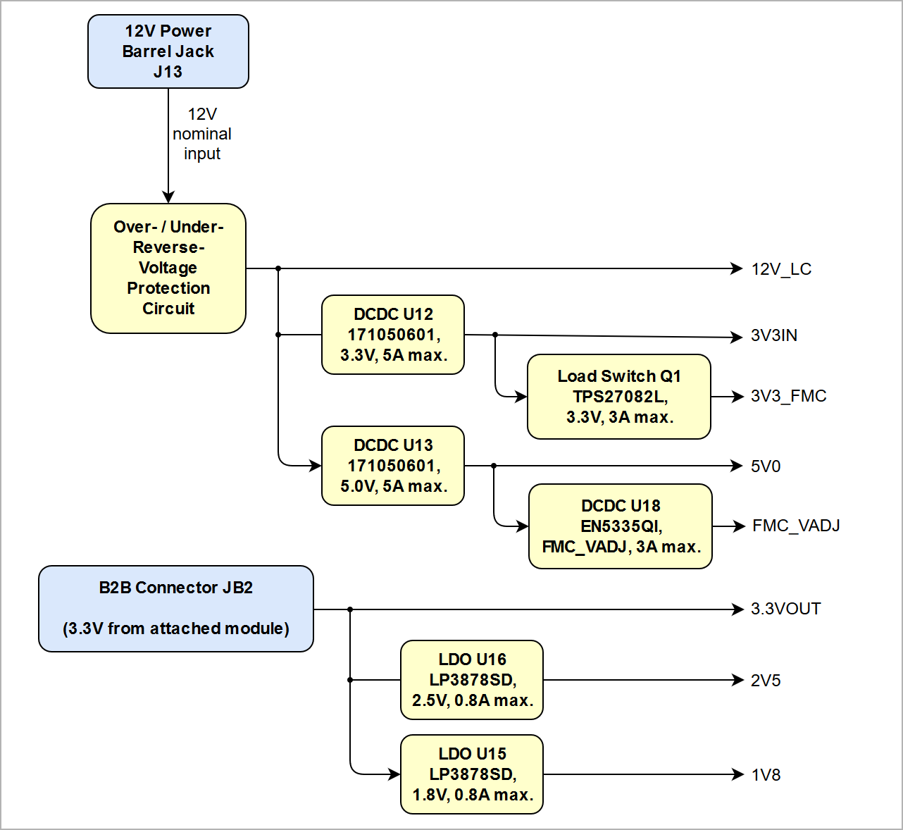 Image Added Image Added
|
|
Power-On Sequence
The on-board voltages 3.3V and 5.0V of the carrier board will be powered up simultaneously when 12V power supply is connected to the barrel jack J10.
The on-board voltages 1.8V and 2.5V will be enabled when module's 3.3V voltage level has become stable and 3.3VOUT is available on the B2B connector JB2 pins 9 and 11.
The PL IO-bank supply voltage FMC_VADJ will be available after the output of the 5.0V DC-DC converter is active and the pin EN_FMC of the System Controller CPLD U14 is asserted.
| Scroll Title |
|---|
| anchor | Figure_PWR_PS |
|---|
| title | Power Sequency |
|---|
|
| Scroll Ignore |
|---|
| draw.io Diagram |
|---|
| border | false |
|---|
| viewerToolbar | true |
|---|
| |
|---|
| fitWindow | false |
|---|
| diagramName | TE0701 power-on sequence diagram |
|---|
| simpleViewer | false |
|---|
| links | auto |
|---|
| tbstyle | hidden |
|---|
| lbox | true |
|---|
| diagramWidth | 641 |
|---|
| revision | 3 |
|---|
|
|
| Scroll Only |
|---|
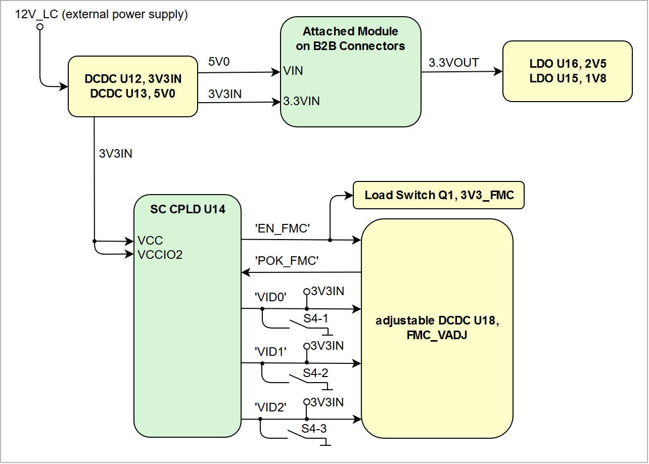 Image Added Image Added
|
|
Configuring mounted SoM's PL bank VCCO FMC_VADJ
On the TE0701 carrier board different VCCIO configurations can be chosen by 7 jumpers and one dedicated 4-bit DIP-switch S4. Settings of the jumpers and the DIP-switch S4 are explained below.
The baseboard supply voltages for the PL IO-banks VCCO of the SoM are selectable by the jumpers J16, J17 and J21. The DIP-switch S4 sets the adjustable baseboard supply-voltage FMC_VADJ.
Following table below describes switch S4 settings for different FMC_VADJ voltages.
| Scroll Title |
|---|
| anchor | Table_PWR_FMC_VADJ |
|---|
| title | Configuring FMC_VADJ |
|---|
|
| Scroll Table Layout |
|---|
| orientation | portrait |
|---|
| sortDirection | ASC |
|---|
| repeatTableHeaders | default |
|---|
| sortByColumn | 1 |
|---|
| sortEnabled | false |
|---|
| cellHighlighting | true |
|---|
|
| S4-1 | S4-2 | S4-3 | FMC_VADJ Value |
|---|
| ON | ON | ON | 3.3V | | OFF | ON | ON | 2.5V | | ON | OFF | ON | 1.8V | | OFF | OFF | ON | 1.5V | | ON | ON | OFF | 1.25V | | OFF | OFF | OFF | Attention: Set VADJ to S3-M1 and S3-M2 control, read TE0701 System Controller CPLD description, before this mode is used! |
|
| Info |
|---|
There is also option to select fixed voltage of FMC_VADJ with the configuration of the 8-bit control register of the I2C-to-GPIO-module of the System Controller CPLD U14. Switch S4 is also routed to the System Controller CPLD, hence the VCCIO configuration can be registered by the SC CPLD. Switch S4-4 is not dedicated for FMC_VADJ setting, the function of this switch depends on the System Controller CPLD firmware. The supply-voltage FMC_VADJ is user programmable via I2C. Configuration of the adjustable voltage FMC_VADJ is done over dedicated I2C bus (lines HDMI_SCL and HDMI_SDA). A control byte has to be sent to the 8-bit control register of the I2C-to-GPIO module of the System Controller CPLD. This modules I2C address is 0x22. To enable FMC_VADJ on TE0701, bit 7 of the control register should be set to 1. Note that the I2C bus is shared with the I2C interface of the HDMI Controller. For detailed information how to set the voltage FMC_VADJ via I2C, please refer to the documentation of the TE0701 System Controller CPLD. |
Configuring 12V Power Supply Pin on the CameraLink Connector
12V power supply can be connected to pin 26 of the CameraLink by closing J18. However, this option is disabled by default (J18: OPEN).
Summary of VCCIO configuration via jumpers
There are two baseboard supply voltages VIOTA and VIOTB connected to the 4 x 5 SoM's PL IO-bank. The supply-voltages have following pin assignments on B2B-connectors:
| Scroll Title |
|---|
| anchor | Table_PWR_VCCIO |
|---|
| title | Baseboard supply-voltages VIOTA and VIOTB |
|---|
|
| Scroll Table Layout |
|---|
| orientation | portrait |
|---|
| sortDirection | ASC |
|---|
| repeatTableHeaders | default |
|---|
| sortByColumn | 1 |
|---|
| sortEnabled | false |
|---|
| cellHighlighting | true |
|---|
|
Baseboard supply voltages | TE0701 B2B connector-pins | Standard 4 x 5 SoM's VCCO pins on B2B connectors | Connected with (Pull-up, VCCIO) |
|---|
| VIOTA | JB2-2, JB2-4, JB2-6 | VCCIOB (JM2-1, JM2-3) / VCCIOC (JM2-5) | HDMI_SCL, HDMI_SDA, HDMI_INT, J5 VCCIO | | VIOTB | JB1-10, JB1-12, JB2-8, JB2-10 | VCCIOA (JM1-9, JM1-11) / VCCIOD (JM2-7, JM2-9) | VCCIO1 (System Controller CPLD pin 55, 73) |
|
| Note |
|---|
Note: The corresponding PL IO-voltage supply voltages of the 4 x 5 SoM to the selectable baseboard voltages VIOTA and VIOTB are depending on the mounted 4 x 5 SoM and varying in order of the used model. Refer to SoM's schematics for more information about the specific pin assignment on module's B2B-connectors regarding PL IO-bank supply voltages and to the 4 x 5 Module integration Guide for VCCIO voltage options. |
Following table shows baseboard supply voltages versus the available voltage levels, which can be configured via jumpers.
Notation: 'Jx: 1-2, 3' means pins 1 and 2 are closed, pin 3 is open. 'Jx: 1, 2-3' means pins 2 and 3 are closed, pin 1 is open.
| Scroll Title |
|---|
| anchor | Table_PWR_JUMPERS |
|---|
| title | Configuration of baseboard supply-voltages via jumpers |
|---|
|
| Scroll Table Layout |
|---|
| orientation | portrait |
|---|
| sortDirection | ASC |
|---|
| repeatTableHeaders | default |
|---|
| sortByColumn | 1 |
|---|
| sortEnabled | false |
|---|
| cellHighlighting | true |
|---|
|
Voltage Levels | VIOTA | VIOTB | USB-VBUS | 12V0_CL |
|---|
| 3V3 | J17:1-2, 3 & J16: open | J17: 1-2, 3 & J16: open & J21:1-2, 3 | - | - | | 2V5 | J17:1, 2-3 & J16: open | J17:1, 2-3 & J16: open & J21: 1-2, 3 | - | - | | FMC_VADJ | J17: open & J16: 1-2 | J21:1, 2-3 | - | - | | 5V0 intern | - | - | J9:1-2, 3 & J19: 1-2 (J20: 1-2: additional decoupling-capacitor 200 µF) | - | | VBUS extern | - | - | J9: 1, 2-3 & J19: open | - | | 12V_LC | - | - | - | J18: 1-2 |
|
| Scroll Title |
|---|
| anchor | Figure_PWR_VCCIO_Jumper |
|---|
| title | VCCIO jumper pin location (PCB-REV06), top view |
|---|
|
 Image Added Image Added
|
| Note |
|---|
Take care of the VCCO voltage ranges of the particular PL IO-banks (HR, HP) of the mounted SoM, otherwise damages may occur to the FPGA. Therefore, refer to the TRM of the mounted SoM to get the specific information of the voltage ranges. It is recommended to set and measure the PL IO-bank supply-voltages before mounting of TE 4 x 5 module to avoid failures and damages to the functionality of the mounted SoM. |
Power Rails
| Scroll Title |
|---|
| anchor | Table_PWR_PR_B2B |
|---|
| title | Power pin description of B2B Module Connector |
|---|
|
| Scroll Table Layout |
|---|
| orientation | portrait |
|---|
| sortDirection | ASC |
|---|
| repeatTableHeaders | default |
|---|
| sortByColumn | 1 |
|---|
| sortEnabled | false |
|---|
| cellHighlighting | true |
|---|
|
| Module Connector (B2B) Designator | VCC / VCCIO | Direction | Pins | Notes |
|---|
| JB1 | 5V0 | Out | 2, 4, 6 | 5.0V module supply voltage | | 3.3VIN | Out | 14, 16 | 3.3V module supply voltage | | VIOTB | Out | 10, 12 | PL IO-bank VCCO | | VIOB | In | 40 | 1.8V module output voltage | | JB2 | 3.3VOUT | In | 9, 11 | 3.3V module output voltage | | 5V0 | Out | 1, 3, 5, 7 | 5.0V module supply voltage | | VIOTA | Out | 2, 4, 6 | PL IO-bank VCCO | | VIOTB | Out | 8, 10 | PL IO-bank VCCO | | VCCJTAG | In | 92 | 3.3V JTAG reference voltage | | JB3 | USB-VBUS | Out | 56 | USB Host supply voltage |
|
| Scroll Title |
|---|
| anchor | Table_PWR_PR_FMC |
|---|
| title | Power pin description of FMC connector |
|---|
|
| Scroll Table Layout |
|---|
| orientation | portrait |
|---|
| sortDirection | ASC |
|---|
| repeatTableHeaders | default |
|---|
| sortByColumn | 1 |
|---|
| sortEnabled | false |
|---|
| cellHighlighting | true |
|---|
|
| FMC Designator | VCC / VCCIO | Direction | Pins | Notes |
|---|
| J10 | 12V_LC | In | Pin C35, C37 | - | | 3V3_FMC | In | Pin D36, D38, D40, C39 | - | | 3.3VOUT | In | Pin D32 | - | | FMC_VADJ | Out | Pin G39, H40 | adjustable FMC VCCIO |
|
| Scroll Title |
|---|
| anchor | Table_PWR_PR_PMOD |
|---|
| title | Power pin description of Pmod connectors |
|---|
|
| Scroll Table Layout |
|---|
| orientation | portrait |
|---|
| sortDirection | ASC |
|---|
| repeatTableHeaders | default |
|---|
| sortByColumn | 1 |
|---|
| sortEnabled | false |
|---|
| cellHighlighting | true |
|---|
|
| PMOD Designator | VCC / VCCIO | Direction | Pins | Notes |
|---|
| J1 | 3.3VOUT | Out | Pin 6, 12 | - | | J2 | 3.3VOUT | Out | Pin 6, 12 | - | | J5 | VIOTA | Out | Pin 6, 12 | - | | J6 | FMC_VADJ | Out | Pin 6, 12 | - |
|
| Scroll Title |
|---|
| anchor | Table_PWR_PR_MAINPWR |
|---|
| title | Power pin description of main power supply connectors |
|---|
|
| Scroll Table Layout |
|---|
| orientation | portrait |
|---|
| sortDirection | ASC |
|---|
| repeatTableHeaders | default |
|---|
| sortByColumn | 1 |
|---|
| sortEnabled | false |
|---|
| cellHighlighting | true |
|---|
|
| Main Power Jack Designator | VCC / VCCIO | Direction | Pins | Notes |
|---|
| J13 | 12VIN | In | 1 | - | | B1 | VBAT | In | + | CR1220 Battery Holder (3.0V) |
|
| Scroll Title |
|---|
| anchor | Table_PWR_PR_PERIPHERALS |
|---|
| title | Power pin description of peripherals' connectors |
|---|
|
| Scroll Table Layout |
|---|
| orientation | portrait |
|---|
| sortDirection | ASC |
|---|
| repeatTableHeaders | default |
|---|
| sortByColumn | 1 |
|---|
| sortEnabled | false |
|---|
| cellHighlighting | true |
|---|
|
| Peripheral Socket Designator | VCC / VCCIO | Direction | Pins | Notes |
|---|
| J15 | FMC_VADJ | In | 1 | ARM JTAG reference voltage VTREF | | J3 | 12V0_CL | In | 1, 26 | 12V CameraLink power supply voltaghe | | J7 | VBUS | In | 1 | USB2.0 device mode USB VBUS | | J4 | 5V_HDMI | Out | 18 | 5V HDMI supply voltage from HDMI Protection Circuit U10 | | J8 | 3.3VOUT | Out | 4 | MicroSD Card Socket | | J12 | USB-VBUS | In / Out | 1 | Direction depends on USB2 mode (OTG, Host, Device mode) |
|
| Scroll Title |
|---|
| anchor | Table_PWR_PR_JUMPERS |
|---|
| title | Power Pin description of VCCIO selection jumpers |
|---|
|
| Scroll Table Layout |
|---|
| orientation | portrait |
|---|
| sortDirection | ASC |
|---|
| repeatTableHeaders | default |
|---|
| sortByColumn | 1 |
|---|
| sortEnabled | false |
|---|
| cellHighlighting | true |
|---|
|
| Jumper / Header Designator | VCC / VCCIO | Direction | Pins | Notes |
|---|
| J17 | VIOTA | In | 2 | - | | 3.3VVOUT | Out | 1 | - | | 2V5 | Out | 3 | - | | J21 | VIOTA | In | 1 | - | | VIOTB | In | 2 | - | | FMC_VADJ | Out | 3 | - | | J16 | FMC_VADJ | Out | 2 | - | | VIOTA | In | 1 | - | | J18 | 12V_LC | Out | 1 | - | | 12V0_CL | In | 2 | - | | J6 | VCCIOC | In | 2, 4, 6 | - | | M1.8VOUT | Out | 1 | - | | J9 | USB-VBUS | In | 2 | - | | VBUS | Out | 3 | 1K13 serial resistor | | VBUS | Out | 1 | 10K serial resistor | | J19 | 5.0V | Out | 1 | 5.0V from USB-VBUS load switch U11 | | VBUS | In | 2 | - | | J20 | 5.0V | In | 1 | USB-VBUS voltage stabilization with
additional 200µF capacitance. | | 5.0V | Out | 2 |
|
Board to Board Connectors
| Page properties |
|---|
|
- This section is optional and only for modules.
- use "include page" macro and link to the general B2B connector page of the module series, for example: 4 x 5 SoM LSHM B2B Connectors
| Include Page |
|---|
| 4 x 5 SoM LSHM B2B Connectors |
|---|
| 4 x 5 SoM LSHM B2B Connectors |
|---|
|
|
| Include Page |
|---|
| 4 x 5 SoM LSHM B2B Connectors |
|---|
| 4 x 5 SoM LSHM B2B Connectors |
|---|
|
Technical Specifications
Absolute Maximum Ratings
| Scroll Title |
|---|
| anchor | Table_TS_AMR |
|---|
| title | Module absolute maximum ratings |
|---|
|
| Scroll Table Layout |
|---|
| orientation | portrait |
|---|
| sortDirection | ASC |
|---|
| repeatTableHeaders | default |
|---|
| sortByColumn | 1 |
|---|
| sortEnabled | false |
|---|
| cellHighlighting | true |
|---|
|
| Parameter | Min | Max | Units | Notes |
|---|
VIN supply voltage | 11.4 | 12.6 | V | ANSI/VITA 57.1 FPGA Mezzanine Card (FMC) standard | | I/O input voltage for SC CPLD U114 | -0.5 | 3.75 | V | Lattice MachXO2 Family datasheet | | Voltage on TXS02612RTWR pins | -0.5 | 3.8 | V | TI TXS02612RTWR data sheet | Storage temperature | -40 | 100 | °C | LED's SML-P11MTT86 data sheet |
|
Recommended Operating Conditions
| Scroll Title |
|---|
| anchor | Table_TS_ROC |
|---|
| title | Recommended Operating Conditions |
|---|
|
| Scroll Table Layout |
|---|
| orientation | portrait |
|---|
| sortDirection | ASC |
|---|
| repeatTableHeaders | default |
|---|
| sortByColumn | 1 |
|---|
| sortEnabled | false |
|---|
| cellHighlighting | true |
|---|
|
| Parameter | Min | Max | Units | Notes |
|---|
| VIN supply voltage | 11.4 | 12.6 | V | - | | I/O input voltage for SC CPLD U14 | -0.3 | 3.6 | V | Lattice MachXO2 Family datasheet | | Voltage on TXS02612RTWR pins | 0 | 3.3 | V | TI TXS02612RTWR data sheet | Operating Temperature Range 1), 2), 3) | 0 | 70 | °C | - |
|
1) Temperature range may vary depending on assembly options
2) The operating temperature range of the onboard peripherals are a junction and also ambient operating temperature ranges
3) The relevant operating temperature range of the overall system is also determined by the operating temperature range of the attached module.
Physical Dimensions
| Scroll Title |
|---|
| anchor | Figure_TS_PD |
|---|
| title | Physical dimensions drawing |
|---|
|
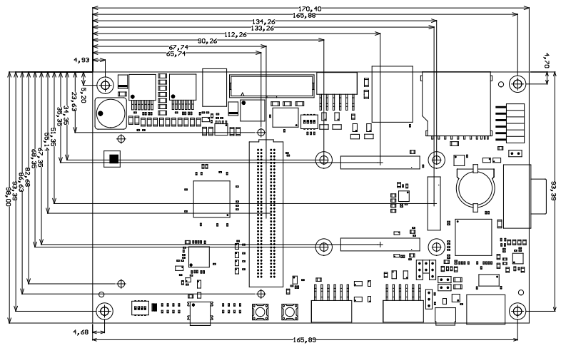 Image Added Image Added |
Variants Currently In Production
| Scroll Title |
|---|
| anchor | Table_VCP_SO |
|---|
| title | Trenz Electronic Shop Overview |
|---|
|
| Scroll Table Layout |
|---|
| orientation | portrait |
|---|
| sortDirection | ASC |
|---|
| repeatTableHeaders | default |
|---|
| sortByColumn | 1 |
|---|
| sortEnabled | false |
|---|
| cellHighlighting | true |
|---|
|
|
Revision History
Hardware Revision History
| Scroll Title |
|---|
| anchor | Table_RH_HRH |
|---|
| title | Hardware Revision History |
|---|
|
| Scroll Table Layout |
|---|
| orientation | portrait |
|---|
| sortDirection | ASC |
|---|
| repeatTableHeaders | default |
|---|
| sortByColumn | 1 |
|---|
| sortEnabled | false |
|---|
| cellHighlighting | true |
|---|
|
|
| Scroll Title |
|---|
| anchor | Figure_RH_HRN |
|---|
| title | Hardware Revision Number |
|---|
|
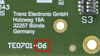 Image Added Image Added |
Hardware revision number is printed on the PCB board next to the module model number separated by the dash.
Document Change History
| Page properties |
|---|
|
- Note this list must be only updated, if the document is online on public doc!
- It's semi automatically, so do following
Add new row below first Copy "Page Information Macro(date)" Macro-Preview, Metadata Version number, Author Name and description to the empty row. Important Revision number must be the same as the Wiki document revision number Update Metadata = "Page Information Macro (current-version)" Preview+1 and add Author and change description. --> this point is will be deleted on newer pdf export template - Metadata is only used of compatibility of older exports
|
| Scroll Title |
|---|
| anchor | Table_RH_DCH |
|---|
| title | Document change history |
|---|
|
| Scroll Table Layout |
|---|
| orientation | portrait |
|---|
| sortDirection | ASC |
|---|
| repeatTableHeaders | default |
|---|
| sortByColumn | 1 |
|---|
| sortEnabled | false |
|---|
| cellHighlighting | true |
|---|
|
| Date | Revision | Authors | Description |
|---|
| Page info |
|---|
| modified-date |
|---|
| modified-date |
|---|
| dateFormat | yyyy-MM-dd |
|---|
|
| | Page info |
|---|
| infoType | Current version |
|---|
| prefix | v. |
|---|
| type | Flat |
|---|
| showVersions | false |
|---|
|
| | Page info |
|---|
| infoType | Modified by |
|---|
| type | Flat |
|---|
| showVersions | false |
|---|
|
| - orrectur JTAGEN description for CPLD/Modul access
| | | | - Corrected USB J9 description
- Typos
- update Button description
- Note for J15
| | v.73 | John Hartfiel | - correction temperature range
| | v.72 | Ali Naseri | - General TRM revision and updated to new style
| | 2018-06-13 | | Ali Naseri | - updated Power-on sequence diagram
| | 2018-01-12 | | John Hartfiel | | | 2017-11-09 | v.60 | John Hartfiel | - add B2B connector section
| | 2017-08-15 | | John Hartfiel | - Add VCCIO Jumper Pin location.
- Updated VADJ description.
| | 2017-08-14 | v.58 | John Hartfiel | | | 2017-05-25 | v.56 | Jan Kumann | - New physical dimensions drawing of the board.
| | 2017-05-16 | | Jan Kumann | - A few overall improvements and corrections, new block diagram.
| | 2017-04-11 | | Ali Naseri | | | 2017-02-15 | | Ali Naseri | - added warning concerning the use of FTDI tools
| | 2017-02-15 | v.40 | Ali Naseri | - added power-on sequence diagram
| | 2017-01-19 | | Ali Naseri | - correction of table 3 (switch-positions to adjust FMC_VADJ)
- inserted hint to set and measure the PL IO-bank supply-voltages
| | 2017-01-13 | | Ali Naseri | - added section for baseboard supply voltage configuration
| | 2016-11-29 | | Ali Naseri | - TRM update due to new revision 06 of
- the carrier board.
| | 2016-11-28 | v.4 | | - TRM adjustment to the newest
- revision (05) of TE0701 Carrier Board.
| | 2014-02-18 | 0.2 | Sven-Ole Voigt | | | 2014-01-05 | 0.1 | Sven-Ole Voigt | |
|
...
Download PDF Version of this Document.
| Scroll pdf ignore |
|---|
Table of Contents |
Overview
| Scroll Only (inline) |
|---|
Online version of this manual and other related documents can be found at https://wiki.trenz-electronic.de/display/PD/TE0701
|
The Trenz Electronic TE0701 Carrier Board is a base-board for 4x5 SoMs, which exposes the MIO- and the PS/PL-pins of the SoM to accessible connectors and provides a whole range of on-board-componentes to test and evaluate Trenz Electronix 4x5 SoMs.See page "4 x 5 cm carriers" to get information about the SoMs supported by the TE0701 Carrier Board.
Main Components
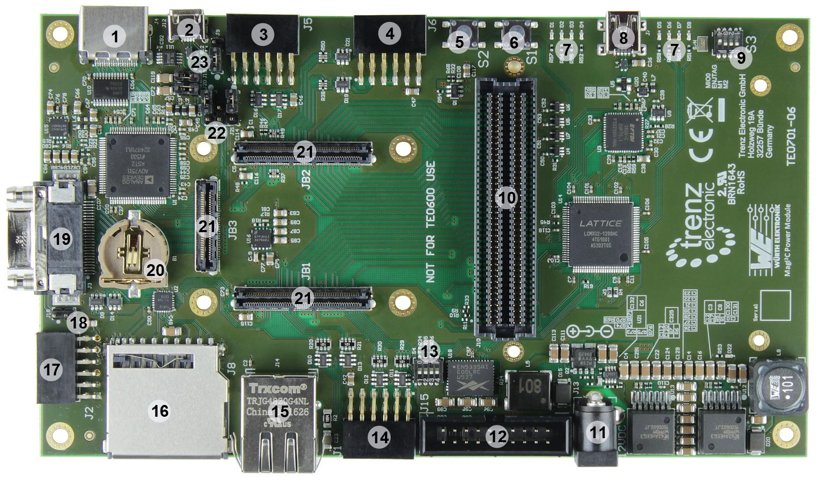 Image Removed
Figure 1: 4x5 SoM carrier board TE0701-06
TE0701-05 (REV 06):
- HDMI Connector (1.4 HEAC Support)
- Micro USB Connector (Device, Host or OTG Modes)
Pmod Connector for Zynq-module PL (4 LVDS-pairs, max. VCCIO-voltage VIOTA)
- Pmod Connector for Zynq-module PL (4 LVDS-pairs, max. VCCIO-voltage FMC_VADJ)
- User Push Button S2 ("RESTART" button by default)
- User Push Button S1 ("RESET" button by default)
- User LEDs (function mapping depends on firmware of System-Controller-CPLD)
- Mini USB Connector (USB JTAG and UART Interface)
- User 4-bit DIP Switch
- VITA 57.1 compliant FMC LPC Connector with digitally programmable FMC VADJ Power Supply
- Barrel jack for 12V Power Supply
- ARM JTAG Connector (DS-5 D-Stream) - PJTAG to EMIO multiplexing needed
- User 4-bit DIP Switch (provides the possibility to set voltage FMC_VADJ)
- Pmod Connector (J1, 3.3V): mapped to 8 Zynq PS MIO0-bank-pins (MIO0, MIO9 to MIO15) when using TE0720 (same mapping as on Zedboard), 6 pins (MIO10 to MIO15) are additionally connected to TE0701 System-Controller-CPLD
- RJ45 GbE Connector
- SD Card Connector - Zynq SDIO0 Bootable SD port
- Pmod Connector (J2, 3.3V): 6 pins (PX0 to PX5) can be multiplexed by Texas Instruments TXS02612RTWR SDIO Port Expander to MIO-pins of Zynq-module, 2 pins are connected to TE0701 System-Controller-CPLD (PX6 and PX7)
- Jumper J18
- Mini CameraLink Connector
- Battery holder for CR1220 (RTC backup voltage)
- Trenz 4x5 module Socket (3x Samtec LSHM Series Connectors)
- Jumper J16, J17, J21
- Jumper J9, J19, J20
Key Features
- Overvoltage-, undervoltage- and reversed- supply-voltage-protection
- Barrel jack for 12V power supply
- Carrier Board System-Controller-CPLD Lattice MachXO2 1200HC, programable by Mini-USB JTAG-Interface J7
- Zynq-module programable by ARM-JTAG-Interface-Connector (J15) or by System-Controller-CPLD via Mini-USB JTAG-Interface J7 or JTAG-Interface on FMC-Connector J10
- Mini CameraLink
- RJ45 Gigabit Ethernet Jack with 2 integrated LEDs.
- FPGA Mezzanine Card (FMC) Connector J10 for acces to Zynq-Module's LVDS-pairs, operable with adjustable IO-voltage FMC_VADJ
- USB JTAG- and UART-Interface (FTDI FT2232HQ) with Mini-USB-Connector J7
- ADV7511 HDMI Transmitter with HDMI-Connector J4
- 8 x user LEDs routed to System-Controller-CPLD, 8 x red
- 2 x user-push button routed to System-Controller-CPLD; by default configured as system "RESET" and "RESTART" button (depends on CPLD-Firmware)
- 2 x 4-bit DIP-Switch for base-board-configuration (3 switches routed to System-Controller-CPLD, 3 switches to set voltage FMC_VADJ, 1 switch routed to Zynq-module (MIO0), 1 switch enables Mini-USB JTAG-Interface J7)
- PMOD-Connectors to access Zynq-Module's LVDS-pairs and MIO-Pins
- Micro SD card socket, can be used to boot system
- Micro-USB-Interface (J12) connected to Zynq-module (Device, Host or OTG modes)
- Trenz 4x5 module Socket (3 x Samtec LSHM series connectors)
Interfaces and Pins
Board to Board (B2B) I/O's
For detailed information about the B2B pin out, please refer to the Master Pinout Table.
Micro SD Card Socket
Micro SD Card socket is not directly wired to the B2B connector pins, but through a Texas Instruments TXS02612 SDIO Port Expander, which is needed for voltage translation due to different voltage levels of the Micro SD Card and MIO-bank of the Xilinx Zynq-module. The Micro SD Card has 3.3V signal voltage level, but the MIO-bank on the Xilinx Zynq-module has VCCIO 1.8V.
The MIO-bank of the Zynq-module is also accessible by PMOD-Connector J2, which is configurable by the "SEL_SD"-signal of the System-Controller-CPLD. The connector J2 has VCCIO 3.3V.
Dual channel USB to UART/FIFO
The TE0701 has on-board USB 2.0 High Speed to UART/FIFO IC FT2232HQ from FTDI. Channel A can be used as JTAG-Interface (MPSSE) to program the System-Controller-CPLD, Channel B can be used as UART-Interface routed to CPLD. There also 4 additionally bus-lanes available for user-specific use. The FT2232HQ-Chip can also be used as FIFO-Buffer.
There is also a standard 256 Byte EEPROM connected to the FT2232HQ-chip available to store custom configuration settings. EEPROM settings can be changed using FTDI provided tools that can be downloaded from FTDI website. See FTDI website for more information.
USB Interface
TE0701 board has two physical USB-connectors:
- J7 as mini-USB-connector wired to on-board FTDI FT2232HQ chip.
- J12 as micro-USB-connector wired to B2B connector JB3 (there is usually an USB-transceiver on the SoMs).
JTAG Interface
JTAG access to the CPLD and Xilinx Zynq-module is provided via Mini-USB JTAG Interface (FTDI FT2232H) and controlled by DIP switch S3.
The JTAG port of the CPLD is enabled by setting switch S3 labeled as "ENJTAG" to the OFF-position.
LED's
There are eight LED's (L1 to L8) available to the user. All LEDs are red colored and connected to the on-board System-Controller-CPLD. Their functions are programmable and depend on the firmware of the System-Controller-CPLD. For detailed information, please refer to the documentation of the TE0701 Sytem-Controller-CPLD.
| Note |
|---|
LED5 (L5) to LED8 (L8) are operating only when the corresponding power supply VIOTB (i.e., bank 1 of the on-board CPLD) is switched on. This can be accomplished on the one hand by connecting the FMC power supply FMC_VADJ to VIOTB (J21: 1,2-3), which is the default option, or on the other hand by connecting either 2.5V (J17: 1,2-3) or 3.3V (J17: 1-2,3) to VIOTB (J21: 1-2,3). Please note that for the first default option, the FMC power supply must be set by the user. For detailed information how to set the voltage FMC_VADJ via I2C, please refer to the documentation of the TE0701 Sytem-Controller-CPLD. |
One green LED D22 shows the availability of the 3.3V supply voltage of the TE0701 Carrier Board.
4-bit DIP-switch
Additionally, on the TE0701 Carrier Board there is a 4-bit DIP-switch (S3; see (9) in Figure 1) available. The default S3 switch mapping is as follows:
...
User-Push-Buttons
On the TE0701 Carrier Board there are two push buttons (S1 and S2) and are routed to the System-Controller-CPLD and available to the user. The default mapping of the push buttons is as follows:
...
If S2 is pushed, the active-high Power ON (PON) signal (that is internally pulled-up) will be deasserted, which can be considered as a "RESTART" button to switch off (push button) and on (release button) all on-module power supplies (except 3.3VIN). Note: The capability to be enabled the first time will become active shortly after Power on Reset (POR).
| Info |
|---|
The active-high PON signal is directly mapped to the active-high EN1 signal which is routed to the SC (e.g., on the TE0720) and directly used (after deglitching) as a mandatory active-high enable signal to the power FET switch (3.3VIN -> 3.3V) as well as the DC-DC converters (VIN -> 1.0V, 1.5V, 1.8V). |
The functionality of the push buttons depends on the CPLD-firmware. For detailed information of the function of the push buttons, please refer to the documentation of the TE0701 Sytem-Controller-CPLD.
Ethernet
TE0701 has a RJ45 Gigabit Ethernet MAGJACK (J14) with two LEDs.
On-board Ethernet jack J14 pins are routed to B2B connector JB1. The center tap of the Magnetics is not connected to module's B2B connector.
PHY LEDs are not connected directly to the module's B2B connectors as the 4x5 module have no dedicated PHY LED pins assigned. PHY LED's are connected to the TE0701 System-Controller-CPLD, that can route those LED's to some module's I/O Pins. In that case the CPLD has to map the PHY LEDs to corresponding pins.
See documentation of the TE0701 Sytem-Controller-CPLD to get information of the function of the PYH LEDs.
Pmod Slots
J5 and J6 Pmod signal routing is done as differential pairs for pins 1-2, 3-4, 7-8, 9-10.
Please use Master Pinout Table table as primary reference for the pin mapping information.
Power
Power Supply
Power supply with minimum current capability of 3A at 12V for system startup is recommended.
TE0701 jumper and DIP switch overview
On the TE0701 carrier boards different VCCIO configurations can be chosen by 7 jumpers and one dedicated 4-bit DIP-switch S4.
The purpose of the jumpers and the DIP-switch S4 of the Carrier Board will be explained in the following sections.
Configuring VCCIO-Voltage
The Zynq-module power supply is fixed to 5V!
...
Furthermore, the VCCIO13 supply voltage (bank 13) can be selected to be either identical to bank 33/34 (J21: 1-2, 3; jumper J16 removed) or to be FMC_VADJ (J21: 1, 2-3). Again, the latter is the default setting (i.e., VCCIO13=FMC_VADJ).
Note: The LVDS-pairs FMC_LA17 to FMC_LA33 (also PB0 to PB3 as well as Y0 to Y5) are routed to bank 13 of the Zynq-module, hence, the VCCIO13 supply voltage is chosen correspondingly by default!
| Info |
|---|
The FMC power supply on the TE0701 Carrier Board (i.e., FMC_VADJ) is user programmable via I2C. The setting of the adjustable voltage FMC_VADJ is done by the dedicated I2C-Bus with the lines "HDMI_SCL" and "HDMI_SDA". Therefore, a control-byte has to be send to the 8-bit control register of the I2C-to-GPIO-module of the System-Controller-CPLD. This module has the I2C-Address 0x22. To enable FMC_VADJ on TE0701, bit 7 of the control-register should be set. Note that the I2C-Bus is shared with the I2C-Interface of the HDMI-Controller. |
| Note |
|---|
There is also the possibility to select fixed FMC_VADJ voltages by the DIP-switch S4. Therefore, there is no need to configure any bits on the 8-bit control register of the I2C-to-GPIO-module of the System-Controller-CPLD. Note: Switch S4-4 is routed to the System-Controller-CPLD, the functionality depends on the CPLD-firmware. |
Table 3 shows the switch-configuration of the DIP-switch S4 to set the voltage FMC_VADJ.
Note: The configuration of FMC_VADJ depends on the used firmware of the System-Controller-CPLD. For detailed information, refer to the documentation of the TE0701 Sytem-Controller-CPLD.
...
S4-1
...
FMC_VADJ Value
...
Table 3: Switch S4 positions for fixed values of the FMC_VADJ voltage
Configuring 12V Power Supply Pin on the CameraLink Connector
Finally, a 12V power supply can be connected to pin 26 of the CameraLink by closing J18. However, this option is disabled by default (J18: OPEN).
Configuring Power Supply of the Micro USB Connector (Device, Host or OTG Modes)
The TE0701 carrier board can be configured as a USB host. Hence, it must provide from 5.25V to 4.75V to the board side of the downstream connection (micro USB port on J12; 13). To provide sufficient power, a TPS2051 power distribution switch is located on the carrier board in between the 5V power supply and the Vbus signal of the USB downstream port interface. If the output load exceeds the current-limit threshold, the TPS2051 limits the output current and pulls the overcurrent logic output (OC_n) low, which is routed to the on-board CPLD. The TPS2051 is put into operation by setting J19 CLOSED. J20 provides an extra 100µF decoupling capacitor (in addition to 10µF) to further stabilize the output signal. Moreover, a series terminating resistor of either 1K (J9: 1-2, 3) or 10K (J9: 1, 2-3) is selectable on the "USB-VBUS" signal. Both signals, USB-VBUS and VBUS_V_EN (that enables the TPS2051 on "high") are routed (as well as the corresponding D+/- data lines) via the on-board connector directly to the USB 2.0 high-speed transceiver PHY from SMSC (USB3320) on the GigaZee module, which is, in turn, connected to the Zynq FPGA. In summary, the default jumper settings are the following: J9: 1-2, 3 (1K series terminating resistor); J19: CLOSED (TPS2051 in operation); J20: CLOSED (100 µF added).
Additionally, the TE0701 carrier board is equipped with a second mini USB port (J7; see (8) in Figure 1) that is connected to a "USB to multi-purpose UART/FIFO IC" from FTDI (FT2232HQ) and provides a USB-to-JTAG interface between a host PC and the TE0701 carrier board and the Zynq-module, respectively. Because it acts as a USB function device, no power switch is required (and only a ESD protection must be provided) in this case.
Power On Reset (POR)
On the TE0701 the 5.0V and 3.3V power supply rails are generated by high performance DC-DC-converters from the external 12V supply. While the 3.3V plane supplies several on-board components (e.g., Lattice CPLD and FTDI Dual USB UART/FIFO IC), the 5V plane is mainly provided to power supply of the module to be carried (e.g., TE0720 Zynq SoC module). For the latter, however, special considerations must be taken (see TE0720 Power Supply). Therefore, the on-module system controller (SC) must be provided with information about the power-on-reset (POR) process, namely, the following control signals EN1, RESIN, and NOSEQ. And the SC provides, in turn, the status signal PGOOD down to the on-board Sytem-Controller-CPLD.
...
This signal is controlled by the user push button S1 on the TE0701 and is forwarded directly to the SC, where it is latched together with the EN1 signal as well as the “all power rails OK” signal (1.0V and 1.8V for core; 1.5V and VTT for RAM, and 3.3V).
| Info |
|---|
The 3.3V power supply rail can be switched on (EN_3V3=’1’) or off (EN_3V3=’0’) by a load switch (TPS27082L) and is continuously checked by a voltage detector (TPS3805H33). Note: The 3.3VIN power supply (from which the 3.3V power plane is sourced) is supplied by the TE0701 Carrier Board and is kept always on! |
When RESIN (alias user push button S1) is not pushed and simultaneously the EN1 signal is asserted (EN='1') and all power rails are ok, the active-high Zynq power-on-reset signal PS_POR_B is asserted.
...
Table 4: Generation of PGOOD-Signal
| Info |
|---|
| For more information on the preceding signals please consult the corresponding Wiki documentation of the TE0720 System Management Controller. |
Technical Specifications
Absolute Maximum Ratings
...
Vin supply voltage
...
11.4
...
V
...
Storage Temperature
...
°C
...
Recommended Operating Conditions
...
Physical Dimensions
Board size: PCB 170.4 mm × 98 mm. Notice that some parts the are hanging slightly over the edge of the PCB like the mini USB-jacks (ca. 1.4 mm), the ethernet RJ-45 jack (ca 2.2 mm) and the mini CameraLink connector (ca. 7 mm), which determine the total phycial demensions of the carrier board. Please download the assembly diagram for exact numbers.
Mating height of the module with standard connectors: 8mm
PCB thickness: ca. 1.65mm
Highest part on the PCB is the ethernet RJ-45 jack, which has an approximately 17 mm overall hight. Please download the step model for exact numbers.
All dimensions are given in mm.
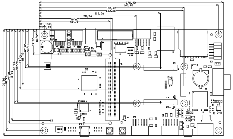 Image Removed
Figure 3: Physical Dimensions of the TE0701-06 carrier board
Operating Temperature Ranges
Commercial grade: 0°C to +70°C.
Board operating temperature range depends also on customer design and cooling solution. Please contact us for options.
Weight
ca. 188 g - Plain board
Document Change History
...
TRM update due to new revision 06 of
the carrier board.
...
...
TRM adjustment to the newest
revision (05) of TE0701 Carrier Board.
...
...
TE0701-03 (REV3) updated
...
0.1
...
Initial release
...
All
...
Hardware Revision History
...
Notes
...
01
...
Prototype
...
additional Jumper J16 and switch S4
for setting VCCIO FMC_VADJ.
...
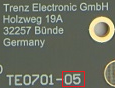 Image Removed
Figure 4: Hardware revision Number
...
Disclaimer
| Include Page |
|---|
| IN:Legal Notices |
|---|
| IN:Legal Notices |
|---|
|