Page History
...
The baseboard supply voltages for the PL IO-banks of the SoM are selectable by the jumpers J16, J17 and J21. The DIP-switch S4 sets the adjustable baseboard supply-voltage FMC_VADJ.
...
| Note |
|---|
There is also option to select fixed voltage of FMC_VADJ with DIP-switch S4. In this case there is no need to configure the 8-bit control register of |
...
the I2C-to-GPIO-module of the System Controller CPLD. |
...
Switch S4 is also routed to the System Controller CPLD, hence the VCCIO configuration can be registered by the CPLD. Switch S4-4 is not dedicated for FMC_VADJ setting, the function of this switch depends on the System Controller CPLD firmware. |
Table 3 below describes switch S4 settings for different FMC_VADJ voltages.
| S4-1 | S4-2 | S4-3 | FMC_VADJ Value |
|---|---|---|---|
| ON | ON | ON | 3.3V |
| OFF | ON | ON | 2.5V |
| ON | OFF | ON | 1.8V |
| OFF | OFF | ON | 1.5V |
| ON | ON | OFF | 1.25V |
| OFF | OFF | OFF | Attention: Set VADJ to S3-M1 and S3-M2 control, read TE0701 System Controller CPLD description, before this mode is used! |
Table 3: Switch S4 positions for fixed values of the FMC_VADJ voltage.
| Info |
|---|
The supply-voltage FMC_VADJ is user programmable via I2C. Configuration of the adjustable voltage FMC_VADJ is done over dedicated I2C bus (lines HDMI_SCL and HDMI_SDA). A control byte has to be sent to the 8-bit control register of the I2C-to-GPIO module of the System Controller CPLD. This modules I2C address is 0x22. To enable FMC_VADJ on TE0701, bit 7 of the control register should be set to 1. Note that the I2C bus is shared with the I2C interface of the HDMI Controller. For detailed information how to set the voltage FMC_VADJ via I2C, please refer to the documentation of the TE0701 System Controller CPLD |
For detailed information how to set the voltage FMC_VADJ via I2C, please refer to the documentation of the TE0701 System Controller CPLD.
| Note |
|---|
There is also option to select fixed voltage of FMC_VADJ with DIP-switch S4. In this case there is no need to configure the 8-bit control register of the I2C-to-GPIO-module of the System Controller CPLD. Switch S4 is also routed to the System Controller CPLD, hence the VCCIO configuration can be registered by the CPLD. Switch S4-4 is not dedicated for FMC_VADJ setting, the function of this switch depends on the System Controller CPLD firmware. |
Table 3 below describes switch S4 settings for different FMC_VADJ voltages.
...
FMC_VADJ Value
...
. |
Configuring 12V Power Supply Pin on the Camera Link Connector
...
There are two baseboard supply voltages VIOTA and VIOTB connected to the 4 x 5 SoM's PL IO-bank. The supply-voltages have following pin assignments on B2B-connectors:
...
Table 4: Baseboard supply-voltages VIOTA and VIOTB
...
Baseboard supply voltages vs voltage levels | VIOTA | VIOTB | USB-VBUS | 12V0_CL |
|---|---|---|---|---|
| 3V3 | J17:1-2, 3 & J16: open | J17: 1-2, 3 & J16: open & J21:1-2, 3 | - | - |
| 2V5 | J17:1, 2-3 & J16: open | J17:1, 2-3 & J16: open & J21: 1-2, 3 | - | - |
| FMC_VADJ | J17: open & J16: 1-2 | J21:1, 2-3 | - | - |
| 5V0 intern | - | - | J9:1-2, 3 & J19: 1-2 (J20: 1-2: additional decoupling-capacitor 100 µF) | - |
| VBUS extern | - | - | J9: 1, 2-3 & J19: open | - |
| 12V_LC | - | - | - | J18: 1-2 |
Table 5: Configuration of baseboard supply-voltages via jumpers. 'Jx: 1-2, 3' means pins 1 and 2 are closed, pin 3 is open. 'Jx: 1, 2-3' means pins 2 and 3 are closed, pin 1 is open.
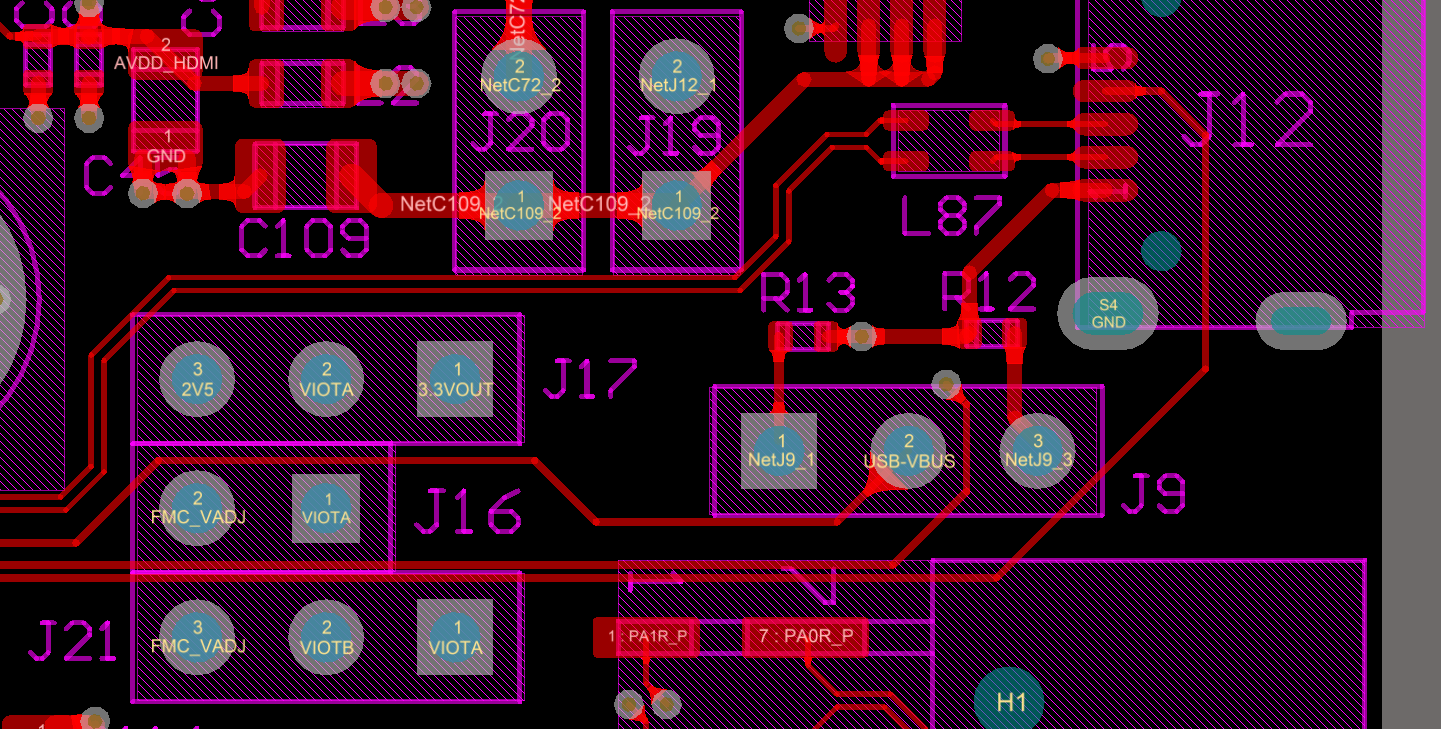
Figure 4: VCCIO jumper pin location (PCB-REV06), top view.
| Note |
|---|
Take care of the VCCO voltage ranges of the particular PL IO-banks (HR, HP) of the mounted SoM, otherwise damages may occur to the FPGA. Therefore, refer to the TRM of the mounted SoM to get the specific information of the voltage ranges. It is recommended to set and measure the PL IO-bank supply-voltages before mounting of TE 4 x 5 module to avoid failures and damages to the functionality of the mounted SoM. |
Technical Specifications
...
All dimensions are given in millimeters.
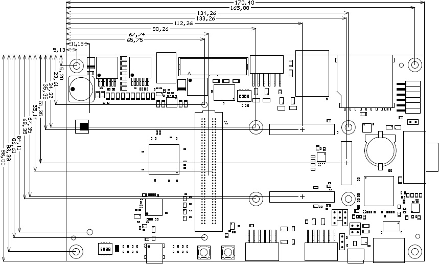
Figure 45: Physical dimensions of the TE0701-06 carrier board.
...
ca. 188 g - Plain board.
Document Change History
| Date | Revision | Authors | Description |
|---|---|---|---|
| 2017-08-15 | John Hartfiel | Add VCCIO Jumper Pin location. Updated VADJ description. | |
| 2017- |
| 08-14 | v.58 | John Hartfiel | Description correction. |
| 2017- |
| 05- |
| 25 | v. |
| 56 | Jan Kumann | New physical dimensions drawing of the board. | |
| 2017-05-16 | v.51 | Jan Kumann | A few overall improvements and corrections, new block diagram. |
| 2017-04-11 |
| Ali Naseri | added block diagram |
| 2017-02-15 | v.45 | Ali Naseri | added warning concerning the use of FTDI tools |
| 2017-02-15 | v.40 | Ali Naseri | added power-on sequence diagram |
| 2017-01-19 | v.35 | Ali Naseri | correction of table 3 (switch-positions to adjust FMC_VADJ) inserted hint to set and measure the PL IO-bank supply-voltages |
| 2017-01-13 | v.20 | Ali Naseri | added section for baseboard supply voltage configuration |
| 2016-11-29 | v.10
| Ali Naseri | TRM update due to new revision 06 of the carrier board. |
| 2016-11-28 | v.4 | Ali Naseri | TRM adjustment to the newest revision (05) of TE0701 Carrier Board. |
| 2014-02-18 | 0.2 | Sven-Ole Voigt | TE0701-03 (REV3) updated |
| 2014-01-05 | 0.1 | Sven-Ole Voigt | Initial release |
| All | Sven-Ole Voigt, Ali Naseri |
Hardware Revision History
...
Overview
Content Tools