Page History
| scroll-ignore |
|---|
Download PDF Version of this Document.
|
| scroll-pdf-ignore | ||||
|---|---|---|---|---|
Table of Contents
|
Overview
| Scroll Only (inline) |
|---|
Online version of this manual and other related documents can be found at https://wiki.trenz-electronic.de/display/PD/TE0600 |
Trenz Electronic GigaBee XC6SLX series are industrial-grade FPGA micromodules integrating a leading-edge Xilinx Spartan-6 LX FPGA, Gigabit Ethernet transceiver (physical layer), two independent banks of 16-bit-wide 128/512 MBytes DDR3 SDRAM, 16 MBytes SPI Flash memory for configuration and operation, and powerful switch-mode power supplies for all on-board voltages. A large number of configurable I/Os is provided via robust board-to-board (B2B) connectors.
...
All this on a tiny footprint, smaller than half a credit card, at the most competitive price.
Block diagram
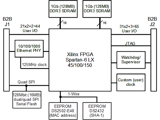
Block diagram of the GigaBee XC6SLX board
Main components
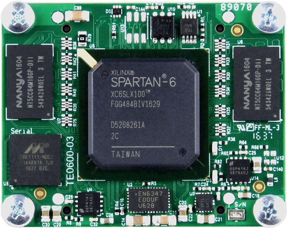
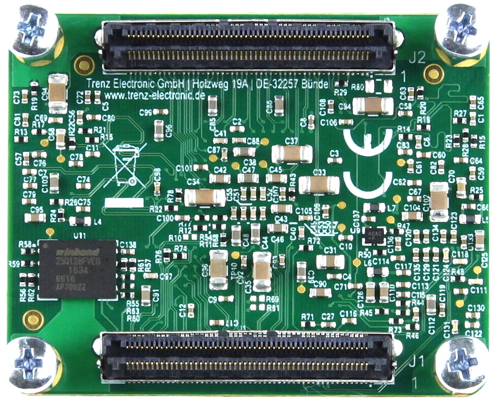
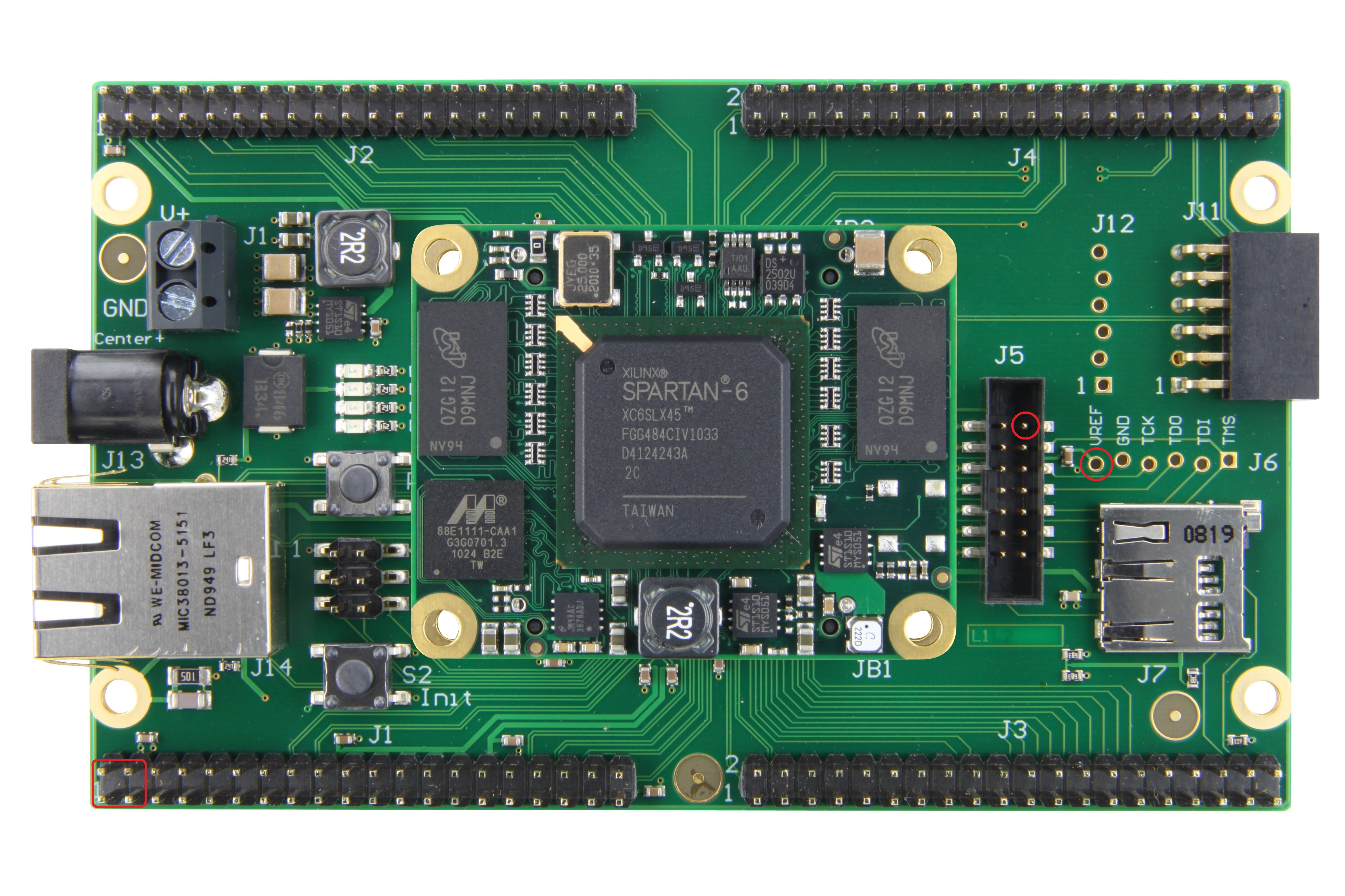
Pictures were photographed from revision 3 and serve for informational purposes only.
Top side:
- Xilinx Spartan-6 LX FPGA
- clock generator
- 10/100/1000 Mbps Ethernet PHY
- protected 1-Wire EEPROM
- DDR3-SDRAM
- DC-DC converters
...
- B2B connector J1
- B2B connector J2
- Flash memory
Key features
Industrial-grade Xilinx Spartan-6 LX FPGA micromodule (LX45 / LX100 / LX150)
10/100/1000 tri-speed Gigabit Ethernet transceiver (PHY)
2 x 16-bit-wide 1 Gb (128 MB) or 4 Gb (512 MB) DDR3 SDRAM
128 Mb (16 MB) SPI Flash memory (for configuration and operation) accessible through:
1 kb protected 1-Wire EEPROM with SHA-1 Engine
JTAG port (SPI indirect)
FPGA configuration through:
B2B connector
JTAG port
SPI Flash memory
Plug-on module with 2 × 100-pin high-speed hermaphroditic strips
Up to 52 differential, up to 109 single-ended (+ 1 dual-purpose) FPGA I/O pins available on B2B strips
46.0 A 0 A x 1.2 V 2 V power rail
3.0 A x 1.5 A x 1.5 V 5 V power rail
- 2x 1A x 2.5V power rail
125 MHz reference clock signal
Single-ended custom oscillator (option)
eFUSE bit-stream encryption (LX100 or larger)
1 user LED
Evenly-spread supply pins for good signal integrity
Additional assembly options are available for cost or performance optimization upon request.
Initial Delivery State
Storage device name | Content | Notes | |
|---|---|---|---|
SPI Flash memory | Blinky Demo | ||
protected 1-Wire EEPROM | not programmed |
Power Consumption
Power consumption of GigaBee XC6SLX modules highly depend on the FPGA design implemented. Some typical power consumptions are provided below for the following reference systems:
Boards – GigaBee XC6SLX 45/100/150
Base board – TE0603-02
Power supply – 5 V from 5 V for baseboard
Connected Gigabit Ethernet cable
| FPGA type | Unconfigured | Configured with Web-server reference design |
|---|---|---|
| LX45 | 0.15 A | 0.6 A |
| LX100 | 0.17 A | 0.5 A |
| LX150 | 0.2 A | 0.5 A |
Detailed Description
Power Supply
The nominal supply voltage of the GigaBee XC6SLX is 3.3 volt. The minimum supply voltage is 3.0 volt. The maximum supply voltage is 3.45 volt.
| Warning | ||
|---|---|---|
| ||
Supply voltages beyond the range might affect to device reliability, or even cause permanent damage of the device! |
Board power supply diagram
Power Supply Sources
GigaBee XC6SLX board must be powered at least in one of the following two ways:
...
Please make sure that your logic design does not draw more RMS current per pin than specified in section Board-to-board Connectors.
FPGA banks VCCIO power supply
FPGA VCCIO power options are shown below. Default values for configurable voltages are shown in braces.
| Bank | Supply voltage |
|---|---|
| B0 | VCCIO 0 VCCIO0 (3. 3 V3V) |
| B1 | VCCIO 1 VCCIO1 (1.5 V5V) |
| B2 | VCCIO2 (3.3 V3V) |
| B3 | VCCIO3 (1.5 V5V) |
Bank 0 power supply VCCIO 0 VCCIO0 can be configured by user to 3.3 V3 V, 2.5 V 5 V or 1.5 V5 V, see Chapter VCCIO0 Power Rail. Bank Banks 1 and 3 VCCIO supply voltage is configured to 1.5 V 5 V to communicate with DDR3 SDRAM memory chip.
By special request, modules can be supplied without DDR3 SDRAM chips. Contact Trenz Electronic support for details.
On-board Power Rails
GigaBee XC6SLX has the following power rails on-board.
| 3.3V Power Rail | It is the main internal power rail and must be supplied from an external power source. It supplies the other following power rails:
|
|---|---|
| 1.2V Power Rail | It is converted from the 3.3V rail by a switching voltage regulator and can provide up to 4.0 A 6A to:
|
| 1.5V Power Rail | It is converted from the 3.3V rail by a switching voltage regulator and can provide up to 1.5 A 3A to:
|
| 2.5V Power Rail | It is converted from the 3.3V rail by a linear voltage regulator and can provide up to 0.8 A 1A to:
|
| VCCAUX Power Rail | It is converted from the 3.3V rail by a linear voltage regulator and can provide up to 0.8 A 1A to:
|
| VCCIO0 Power Rail | There are 4 options to supply this rail:
It supplies:
Figure below show simplified schematic of power options. Dashed resistors are not populated by default.
|
...
power-rail | nominal | maximum | power | system | user |
|---|---|---|---|---|---|
| 3.3V | 3.3 | 2.4 | J1, J2 | module | J1 (≤1.2 A) |
| 2.5V | 2.5 | 1.0.8 | 3.3V ? linear | Ethernet | J1 (≤0.3 A) |
| 1.5V | 1.51 | 3.50 | 3.3V ? switch | DDR3 SDRAM | J1 (≤0.3 A) |
| 1.2V | 1.2 | 46.0 | 3.3V ? switch | VCCINT | J1 (≤0.6 A) |
| VCCAUX | 2.5 | 1.0.8 | 3.3V ? linear | FPGA | J2 (≤0.3 A) |
| VCCCIO0 | 1.2, 1.5, 1.8, 2.5, 3.3 | 0.9 | J2 or 2.5V or 3.3V | VCCO (0) | J2 (≤0.9 A) |
Power Supervision
Power-on Reset
During power-on, the /RESET line is first asserted. Thereafter, the supply voltage supervisor monitors the power supply rail 3.3V and keeps the /RESET line active (low) as long as the supply rail remains below the threshold voltage (2.93 volt). An internal timer delays the return of the /RESET line to the inactive state (high) to ensure proper system reset prior to a regular system start-up. The typical delay time td of 200 ms starts after the supply rail has risen above the threshold voltage.
...
After this delay, the /RESET line is reset (high) and the FPGA configuration can start. When the supply rail voltage drops below the threshold voltage, the /RESET line becomes active (low) again and stays active (low) as long as the rail voltage remains below the threshold voltage (2.93 volt). Once the rail voltage raises again and remains over the threshold voltage for more than the typical delay time td of 200 ms, the /RESET line returns to the inactive state (high) to allow a new system start-up.
Power Fail
GigaBee XC6SLX integrates a power-fail comparator which can be used for low-battery detection, power-fail warning, or for monitoring a power supply other than the main supply 3.3 V. When the voltage of the PFI (power-fail comparator input, input pin 16 of connector J2) line drops below 1.25 volt, the /PFO (power-fail comparator output, FPGA pin A2, label IO_L83P_3) line becomes active (low). The user application can sense this line to take action. To set a power fail threshold higher than 1.25 volt, the user can implement a simple resistive voltage divider on the carrier board.
Board-to-board Connectors
| Include Page | ||||||
|---|---|---|---|---|---|---|
|
EPROM
GigaBee XC6SLX board contains a Maxim DS2502-E48 node address chip with factory-programmed valid MAC-48 address and 768 bits of OTP-EPROM memory for user data.
...
More information can be found at the Maxim DS2432 product page.
DDR3 SDRAM Memory
The board contains two 1 Gb (128 MB) or 4 Gb (512 MB) DDR3 SDRAM chips. Data width of each chip is 16 bit. DDR3 memory connected to FPGA bank 1 and FPGA bank 3. Spartan-6 Memory controller Blocks operations can be merged to implement effective 32-bit memory interface. Refer Xilinx XAPP496 for detailed information.
Flash Memory
GigaBee XC6SLX board contains 128 Mb (16 MB) serial flash memory chip Winbond W25Q128FV (W25Q128BV till REV 02) (U11). This serial flash chip can operate as general SPI memory mode and in double or quad modes. Usage of dual and quad modes increase bandwidth up to 40 MB/s.
For more information see Winbond W25Q128FV W25Q128JVEIQ (W25Q128BV till REV 02or W25Q128FV in old revisions) product overview.
Flash can be programmed in several ways:
...
Serial flash signals connection
Ethernet
The board contains a Marvell Alaska Ethernet PHY chip (88E1111) operating at 10/100/1000 Mb/s. The board supports GMII interface mode with the FPGA. Configuration details:
...
| Note | ||
|---|---|---|
| ||
For correct operation of the Marvell PHY it is required that PHY Reset pin sees valid low level each time power is applied and also during any brownout situations where system Power is removed for short time, but some pins are not at valid logic levels. Solutions:
Explanation: Marvell PHY samples the MODE pins ONLY when it sees low level on PHY reset input, it does not sample those pins during short power off situations (if the reset pin holds high level because of pin capacitance and high impedance of the pins)! So it is possible that the PHY mode is reset, but the mode pins are not sampled again - this yields in mode setting where 125MHz reference clock from PHY is not available. |
Oscillators
The module has one 25 MHz oscillator for Ethernet PHY (U9). Ethernet PHY provides clock multiplication and resulting 125 MHz clock acts as a system and user clock for the FPGA (FPGA input pin AA12).
| Note | ||
|---|---|---|
| ||
Note: For correct generation start, PHY should receive reset pulse. Recommended way to do it it's to connect PHY reset signal (ETHERNET_PHY_RST_N) to LOCKED output of corresponding DCM (DCM which use 125 MHz from PHY). |
The module also provides the footprint for custom additional 3.3 V 3 V single-ended oscillator (U12) which can be installed as an option used as a system and user clock for the FPGA (FPGA input pin Y13).
User LED
The module contains one user active-low LED connected to FPGA output pin T20. To access more LEDs, use a carrier board and drive FPGA signals connected to B2B connectors. As LED connected to FPGA bank with configurable VCCIO to light LED FPGA pin should in '0' (low) state. To disable LED FPGA pin should be in 'Z' (High impedance).
Watchdog
GigaBee XS6LX has a watchdog timer that is periodically triggered by a positive or negative transition of the WDI (watchdog input) line (FPGA pin V9). When the supervising system fails to re-trigger the watchdog circuit within the time-out interval (min 1.1 s, typ 1.6 s, max 2.3 s), the /WDO (watchdog output) line becomes active (low). This event also re-initializes the watchdog timer.
...
Unused IOB Pins option selection.
In the standard assembly, the /WDO (watchdog output) line is left unconnected1 and the only possibility to reset the module is by driving the /MR (master reset) line active (low) through pin 18 of connector J2.
...
| Note | ||
|---|---|---|
| ||
If alternate assembly is used, pin 18 of connector J2 must be left unconnected. |
Configuration Options
The FPGA on GigaBee XC6SLX board can be configured by means of the following devices:
- Xilinx download cable (JTAG)
- SPI Flash memory
JTAG Configuration
The FPGA can be configured through the JTAG interface. JTAG signals are connected to B2B connector J2. When GigaBee XC6SLX board is used with the TE0603 carrier board, the JTAG interface can be accessed via connectors J5 and J6 on the carrier board.
Flash Configuration
Default configuration option for FPGA is “Master Serial/SPI”. The bit-stream for the FPGA is stored in a serial Flash chip (U11). See chapter 2.7 Flash Memory for additional information.
eFUSE Programming
eFUSE programming feature is not directly supported by GigaBee XC6SLX modules, but it is possible to use it. To program eFUSE, please follow the steps below:
- Connect VCCAUX to 3.3V power rail.
On TE0603 it can be done by connecting J5 pin 2 or J6 “VREF” (VCCAUX) to J1 any pin from 1,2,3,4 (3.3V). See Figure below. - Program eFUSE using JTAG cable and iMPACT software.
- Remove power supply connections to VCCAUX
B2B Connectors Pin Descriptions
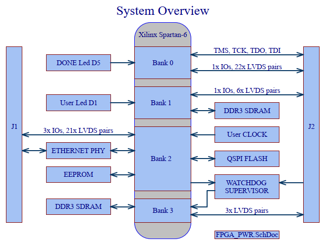
This section describes how the various pins on B2B connectors J1 and J2 connects to TE0600 on-board components. There are five main signal types connected to B2B connectors:
...
| FPGA Bank | Single-ended | Differential | Total | VCCIO | |
| Bank 0 | 1 | 22 | 45 | VCCIO 0 VCCIO0 (3.3 V3V) | |
| Bank 1 | 1 | 6 | 13 | VCCIO 1 VCCIO1 (1.5 V5V) | |
| Bank 2 | 3 | 21 | 45 | VCCIO2 (3.3 V3V) | |
| Bank 3 | 0 | 3 | 6 | VCCIO3 (1.5 V5V) | |
| 5 | 52 | 109 |
B2B signals count
Pin Labeling
FPGA user signals connected to B2B connectors are characterized by the "B2B_Bx_Lyy_p" naming convention, where:
...
Remaining signals use custom names.
Pin Numbering
Note that GigaBee XC6SLX have hermaphroditic B2B connectors. A feature of hermaphroditic connector numbering is that connected signal numbers don't match. Odd signals on module connect to even signals on baseboard. For example module signal 1 to baseboard signal 2, module signal 2 to baseboard signal 1, module signal 3 to baseboard signal 4 and so on.
Pin Types
Most pins of B2B connectors J1 and J2 are general-purpose, user-defined I/O pins (GPIOs). There are, however, up to 8 different functional types of pins on the TE0600, as outlined in Table below. In pin-out tables Table 11 and Table 12, the individual pins are colour-coded according to pin type as in Table below.
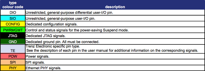
TE0600 pin types
| type colour code | description |
|---|---|
| DIO | Unrestricted, general-purpose differential user-I/O pin. |
| SIO | Unrestricted, general-purpose user-I/O pin. |
| CONFIG | Dedicated configuration signals. |
| PWRMGMT | Control and status signals for the power-saving Suspend mode. |
| JTAG | Dedicated JTAG signals. |
| GND | Dedicated ground pin. All must be connected. |
| TE | Trenz Electronic specific pin type. See the description of each pin in the user manual for additional information on the corresponding signals. |
| POW | Power signals. |
| SPI | SPI signals. |
| PHY | Ethernet PHY signals. |
...
See “Spartan-6 FPGA SelectIO Resources” page 38 for detailed information.
External Bank 2 differential clock connection
TE0600 -02 module have optional connection to FPGA bank 2 differential clock input pins. To provide connection from B2B_B2_L41_P signal to Y13 FPGA pin, zero-resistor R69 should be soldered. To provide connection B2B_B2_L41_N signal to AB13 FPGA pin, zero-resistor R81 should be soldered. Note that in this case optional user oscillator U13 can't be used.
J1 Pin-out
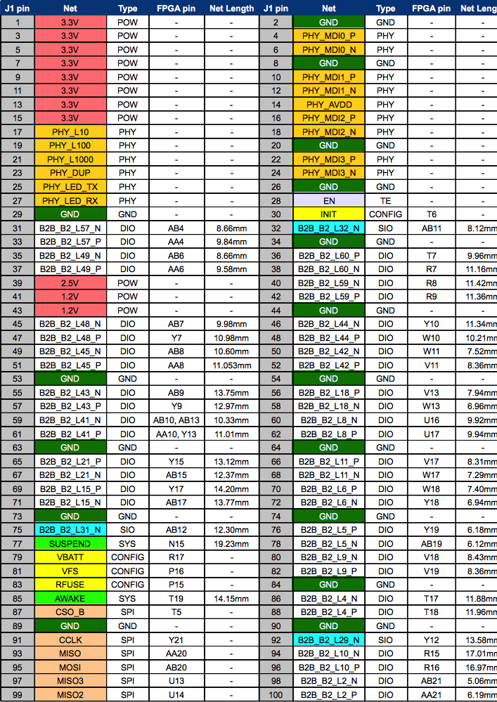
J1 pin-out
| J1 pin | Net | Type | FPGA pin | Net Length | J1 pin | Net | Type | FPGA pin | Net Length |
| 1 | 3.3V | POW | - | - | 2 | GND | GND | - | - |
| 3 | 3.3V | POW | - | - | 4 | PHY_MDI0_P | PHY | - | - |
| 5 | 3.3V | POW | - | - | 6 | PHY_MDI0_N | PHY | - | - |
| 7 | 3.3V | POW | - | - | 8 | GND | GND | - | - |
| 9 | 3.3V | POW | - | - | 10 | PHY_MDI1_P | PHY | - | - |
| 11 | 3.3V | POW | - | - | 12 | PHY_MDI1_N | PHY | - | - |
| 13 | 3.3V | POW | - | - | 14 | PHY_AVDD | PHY | - | - |
| 15 | 3.3V | POW | - | - | 16 | PHY_MDI2_P | PHY | - | - |
| 17 | PHY_L10 | PHY | - | - | 18 | PHY_MDI2_N | PHY | - | - |
| 19 | PHY_L100 | PHY | - | - | 20 | GND | GND | - | - |
| 21 | PHY_L1000 | PHY | - | - | 22 | PHY_MDI3_P | PHY | - | - |
| 23 | PHY_DUP | PHY | - | - | 24 | PHY_MDI3_N | PHY | - | - |
| 25 | PHY_LED_TX | PHY | - | - | 26 | GND | GND | - | - |
| 27 | PHY_LED_RX | PHY | - | - | 28 | EN | TE | - | - |
| 29 | GND | GND | - | - | 30 | INIT | CONFIG | T6 | - |
| 31 | B2B_B2_L57_N | DIO | AB4 | 812.66mm3056mm | 32 | B2B_B2_L32_N | SIO | AB11 | 89.12mm2307mm |
| 33 | B2B_B2_L57_P | DIO | AA4 | 912.84mm3446mm | 34 | GND | GND | - | - |
| 35 | B2B_B2_L49_N | DIO | AB6 | 810.66mm9076mm | 36 | B2B_B2_L60_P | DIO | T7 | 912.96mm8674mm |
| 37 | B2B_B2_L49_P | DIO | AA6 | 911.58mm4038mm | 38 | B2B_B2_L60_N | DIO | R7 | 1113.16mm3583mm |
| 39 | 2.5V | POW | - | - | 40 | B2B_B2_L59_N | DIO | R8 | 1113.42mm4941mm |
| 41 | 1.2V | POW | - | - | 42 | B2B_B2_L59_P | DIO | R9 | 1113.36mm4584mm |
| 43 | 1.2V | POW | - | - | 44 | GND | GND | - | - |
| 45 | B2B_B2_L48_N | DIO | AB7 | 914.98mm447mm | 46 | B2B_B2_L44_N | DIO | Y10 | 1113.34mm4331mm |
| 47 | B2B_B2_L48_P | DIO | Y7 | 1014.98mm6069mm | 48 | B2B_B2_L44_P | DIO | W10 | 1013.21mm0478mm |
| 49 | B2B_B2_L45_N | DIO | AB8 | 1011.60mm3986mm | 50 | B2B_B2_L42_N | DIO | W11 | 79.52mm889mm |
| 51 | B2B_B2_L45_P | DIO | AA8 | 11.053mm642mm | 52 | B2B_B2_L42_P | DIO | V11 | 810.36mm2701mm |
| 53 | GND | GND | - | - | 54 | GND | GND | - | - |
| 55 | B2B_B2_L43_N | DIO | AB9 | 13.75mm1392mm | 56 | B2B_B2_L18_P | DIO | V13 | 710.94mm5384mm |
| 57 | B2B_B2_L43_P | DIO | Y9 | 1213.97mm5123mm | 58 | B2B_B2_L18_N | DIO | W13 | 610.96mm0455mm |
| 59 | B2B_B2_L41_N | DIO | AB10, AB13 | 1015.33mm7999mm | 60 | B2B_B2_L8_N | DIO | U16 | 912.92mm2993mm |
| 61 | B2B_B2_L41_P | DIO | AA10, Y13 | 1116.01mm1771mm | 62 | B2B_B2_L8_P | DIO | U17 | 912.94mm2993mm |
| 63 | GND | GND | - | - | 64 | GND | GND | - | - |
| 65 | B2B_B2_L21_P | DIO | Y15 | 1314.12mm8399mm | 66 | B2B_B2_L11_P | DIO | V17 | 810.31mm5343mm |
| 67 | B2B_B2_L21_N | DIO | AB15 | 1214.37mm6254mm | 68 | B2B_B2_L11_N | DIO | W17 | 710.29mm1532mm |
| 69 | B2B_B2_L15_P | DIO | Y17 | 1413.20mm2958mm | 70 | B2B_B2_L6_P | DIO | W18 | 79.40mm5851mm |
| 71 | B2B_B2_L15_N | DIO | AB17 | 13.77mm1454mm | 72 | B2B_B2_L6_N | DIO | Y18 | 69.94mm1811mm |
| 73 | GND | GND | - | - | 74 | GND | GND | - | - |
| 75 | B2B_B2_L31_N | SIO | AB12 | 1214.30mm3436mm | 76 | B2B_B2_L5_P | DIO | Y19 | 68.18mm398mm |
| 77 | SUSPEND | SYS | N15 | 1921.23mm1709mm | 78 | B2B_B2_L5_N | DIO | AB19 | 68.12mm3535mm |
| 79 | VBATT | CONFIG | R17 | - | 80 | B2B_B2_L9_N | DIO | V18 | 810.43mm2621mm |
| 81 | VFS | CONFIG | P16 | - | 82 | B2B_B2_L9_P | DIO | V19 | 810.36mm1752mm |
| 83 | RFUSE | CONFIG | P15 | - | 84 | GND | GND | - | - |
| 85 | AWAKE | SYS | T19 | 1416.15mm1634mm | 86 | B2B_B2_L4_N | DIO | T17 | 1113.88mm4321mm |
| 87 | CSO_B | SPI | T5 | - | 88 | B2B_B2_L4_P | DIO | T18 | 1113.96mm8014mm |
| 89 | GND | GND | - | - | 90 | GND | GND | - | - |
| 91 | CCLK | SPI | Y21 | - | 92 | B2B_B2_L29_N | SIO | Y12 | 1315.58mm9734mm |
| 93 | MISO | SPI | AA20 | - | 94 | B2B_B2_L10_N | DIO | R15 | 1718.01mm4735mm |
| 95 | MOSI | SPI | AB20 | - | 96 | B2B_B2_L10_P | DIO | R16 | 1618.97mm3045mm |
| 97 | MISO3 | SPI | U13 | - | 98 | B2B_B2_L2_N | DIO | AB21 | 58.06mm425mm |
| 99 | MISO2 | SPI | U14 | - | 100 | B2B_B2_L2_P | DIO | AA21 | 68.19mm4085mm |
J2 Pin-out
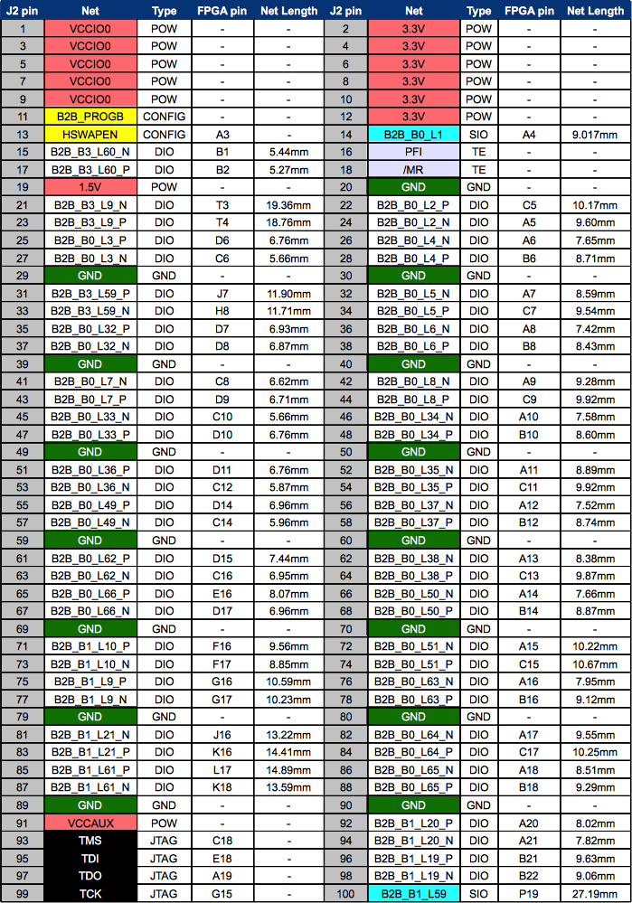
J2 Pin-out
| J2 pin | Net | Type | FPGA pin | Net Length | J2 pin | Net | Type | FPGA pin | Net Length |
| 1 | VCCIO0 | POW | - | - | 2 | 3.3V | POW | - | - |
| 3 | VCCIO0 | POW | - | - | 4 | 3.3V | POW | - | - |
| 5 | VCCIO0 | POW | - | - | 6 | 3.3V | POW | - | - |
| 7 | VCCIO0 | POW | - | - | 8 | 3.3V | POW | - | - |
| 9 | VCCIO0 | POW | - | - | 10 | 3.3V | POW | - | - |
| 11 | B2B_PROGB | CONFIG | - | - | 12 | 3.3V | POW | - | - |
| 13 | HSWAPEN | CONFIG | A3 | - | 14 | B2B_B0_L1 | SIO | A4 | 9.017mm4715mm |
| 15 | B2B_B3_L60_N | DIO | B1 | 57.44mm5418mm | 16 | PFI | TE | - | - |
| 17 | B2B_B3_L60_P | DIO | B2 | 56.27mm7655mm | 18 | /MR | TE | - | - |
| 19 | 1.5V | POW | - | - | 20 | GND | GND | - | - |
| 21 | B2B_B3_L9_N | DIO | T3 | 1921.36mm4246mm | 22 | B2B_B0_L2_P | DIO | C5 | 1012.17mm0314mm |
| 23 | B2B_B3_L9_P | DIO | T4 | 1821.76mm2943mm | 24 | B2B_B0_L2_N | DIO | A5 | 911.60mm8853mm |
| 25 | B2B_B0_L3_P | DIO | D6 | 69.76mm0158mm | 26 | B2B_B0_L4_N | DIO | A6 | 710.65mm8292mm |
| 27 | B2B_B0_L3_N | DIO | C6 | 58.66mm4466mm | 28 | B2B_B0_L4_P | DIO | B6 | 811.71mm2228mm |
| 29 | GND | GND | - | - | 30 | GND | GND | - | - |
| 31 | B2B_B3_L59_P | DIO | J7 | 1114.90mm0801mm | 32 | B2B_B0_L5_N | DIO | A7 | 811.59mm7078mm |
| 33 | B2B_B3_L59_N | DIO | H8 | 1113.71mm8896mm | 34 | B2B_B0_L5_P | DIO | C7 | 911.54mm9983mm |
| 35 | B2B_B0_L32_P | DIO | D7 | 69.93mm1276mm | 36 | B2B_B0_L6_N | DIO | A8 | 710.42mm6094mm |
| 37 | B2B_B0_L32_N | DIO | D8 | 69.87mm1646mm | 38 | B2B_B0_L6_P | DIO | B8 | 810.43mm9961mm |
| 39 | GND | GND | - | - | 40 | GND | GND | - | - |
| 41 | B2B_B0_L7_N | DIO | C8 | 69.62mm1167mm | 42 | B2B_B0_L8_N | DIO | A9 | 912.28mm2657mm |
| 43 | B2B_B0_L7_P | DIO | D9 | 69.71mm3073mm | 44 | B2B_B0_L8_P | DIO | C9 | 912.92mm5699mm |
| 45 | B2B_B0_L33_N | DIO | C10 | 58.66mm889mm | 46 | B2B_B0_L34_N | DIO | A10 | 711.58mm7216mm |
| 47 | B2B_B0_L33_P | DIO | D10 | 69.76mm1201mm | 48 | B2B_B0_L34_P | DIO | B10 | 811.60mm6163mm |
| 49 | GND | GND | - | - | 50 | GND | GND | - | - |
| 51 | B2B_B0_L36_P | DIO | D11 | 68.76mm6976mm | 52 | B2B_B0_L35_N | DIO | A11 | 812.89mm4283mm |
| 53 | B2B_B0_L36_N | DIO | C12 | 58.87mm3601mm | 54 | B2B_B0_L35_P | DIO | C11 | 912.92mm6535mm |
| 55 | B2B_B0_L49_P | DIO | D14 | 69.96mm136mm | 56 | B2B_B0_L37_N | DIO | A12 | 710.52mm7513mm |
| 57 | B2B_B0_L49_N | DIO | C14 | 58.96mm7449mm | 58 | B2B_B0_L37_P | DIO | B12 | 811.74mm0849mm |
| 59 | GND | GND | - | - | 60 | GND | GND | - | - |
| 61 | B2B_B0_L62_P | DIO | D15 | 79.44mm687mm | 62 | B2B_B0_L38_N | DIO | A13 | 812.38mm5431mm |
| 63 | B2B_B0_L62_N | DIO | C16 | 69.95mm5212mm | 64 | B2B_B0_L38_P | DIO | C13 | 912.87mm8448mm |
| 65 | B2B_B0_L66_P | DIO | E16 | 810.07mm0885mm | 66 | B2B_B0_L50_N | DIO | A14 | 711.66mm3259mm |
| 67 | B2B_B0_L66_N | DIO | D17 | 69.96mm9228mm | 68 | B2B_B0_L50_P | DIO | B14 | 811.87mm4909mm |
| 69 | GND | GND | - | - | 70 | GND | GND | - | - |
| 71 | B2B_B1_L10_P | DIO | F16 | 911.56mm3734mm | 72 | B2B_B0_L51_N | DIO | A15 | 1012.22mm0938mm |
| 73 | B2B_B1_L10_N | DIO | F17 | 811.85mm466mm | 74 | B2B_B0_L51_P | DIO | C15 | 1012.67mm5055mm |
| 75 | B2B_B1_L9_P | DIO | G16 | 1012.59mm5086mm | 76 | B2B_B0_L63_N | DIO | A16 | 711.95mm3551mm |
| 77 | B2B_B1_L9_N | DIO | G17 | 1012.23mm6008mm | 78 | B2B_B0_L63_P | DIO | B16 | 911.12mm772mm |
| 79 | GND | GND | - | - | 80 | GND | GND | - | - |
| 81 | B2B_B1_L21_N | DIO | J16 | 1315.22mm7408mm | 82 | B2B_B0_L64_N | DIO | A17 | 913.55mm5157mm |
| 83 | B2B_B1_L21_P | DIO | K16 | 1415.41mm9404mm | 84 | B2B_B0_L64_P | DIO | C17 | 1013.25mm4806mm |
| 85 | B2B_B1_L61_P | DIO | L17 | 1417.89mm852mm | 86 | B2B_B0_L65_N | DIO | A18 | 812.51mm4997mm |
| 87 | B2B_B1_L61_N | DIO | K18 | 1317.59mm4155mm | 88 | B2B_B0_L65_P | DIO | B18 | 912.29mm3889mm |
| 89 | GND | GND | - | - | 90 | GND | GND | - | - |
| 91 | VCCAUX | POW | - | - | 92 | B2B_B1_L20_P | DIO | A20 | 811.02mm0846mm |
| 93 | TMS | JTAG | C18 | - | 94 | B2B_B1_L20_N | DIO | A21 | 710.82mm7172mm |
| 95 | TDI | JTAG | E18 | - | 96 | B2B_B1_L19_P | DIO | B21 | 912.63mm0803mm |
| 97 | TDO | JTAG | A19 | - | 98 | B2B_B1_L19_N | DIO | B22 | 911.06mm8608mm |
| 99 | TCK | JTAG | G15 | - | 100 | B2B_B1_L59 | SIO | P19 | 2730.19mm179mm |
Signal Integrity Considerations
Traces of differential signals pairs are routed symmetrically (as symmetric pairs).
Traces of differential signals pairs are NOT routed with equal length, although difference in signal lines length is negligible for actual signal frequencies. For applications where traces length has to be matched or timing differences have to be compensated, Tables below abowe list the trace length of I/O signal lines measured from FPGA balls to B2B connector pins.
...
An electronic version of these pin-out tables are available for download from the Trenz Electronic support area of the web site.
Module revisions and assembly variants
Module revision coded by 4 FPGA BR[3:0] pins, which can be read by FPGA firmware. All these pins should be configured to have internal PULLUP.
| Signal FPGA pin | BR3 R19 | BR2 P18 | BR1 N16 | BR0 P17 |
|---|---|---|---|---|
| Revision 01 | 1 | 1 | 1 | 1 |
| Revision 02 | 1 | 1 | 1 | 0 |
| Revision 03 | 1 | 1 | 0 | 1 |
| Revision 04 | 1 | 1 | 0 | 0 |
Board revisions pin coding
Main differences between 01 and 02 revisions:
...
- Optimized placement and routing for DC/DC converters
- Added thermal vias to mounting holes
- Added Testpoints
- Changed Board revision identification to REV03
- Changed U9 from SIT1602AI-83-33E-25.0000 to SiT8008AI-73-XXS-25.000000E
- Added Track-it™ Traceability Pad
- Change SPI Flash from W25Q128BVEIG to W25Q128FVEIG
- DDR3 changed from IM4G16D3EABG-125I to IM4G16D3FABG-125I for the 4 GBit variants
- U13 (DS2432P+) is no longer populated by default
...
Main differences between 03 and 04 revisions:
- Optimized placement and routing
- More powerful regulators
- Removed stucked vias
- Added Testpoints
- Changed Board revision identification to REV04
- U12 was fitted for all module assembly variants as default
Module assembly variants coded by 4 zero ohm resistors, connected to FPGA AV[3:0] pins. All these pins should be configures configured to have internal PULLUP.
| Signal FPGA pin | AV3 M18 | AV2 M17 | AV1 V20 | AV0 U19 | Speed grade | SDRAM | Temp grade | Status |
|---|---|---|---|---|---|---|---|---|
| TE0600-02[V|B] | 0 | 0 | 0 | 0 | 2 | 2x128MBit | C | obsolete |
| TE0600-02[V|B]I | 0 | 0 | 0 | 1 | 2 | 2x128MBit | I | obsolete |
| TE0600-02[V|B]F | 0 | 0 | 1 | 0 | 3 | 2x128MBit | C | obsolete |
| TE0600-02[V|B]IF | 0 | 0 | 1 | 1 | 3 | 2x128MBit | I | obsolete |
| TE0600-02[V|B]MF | 0 | 1 | 0 | 0 | 3 | 2x512MBit | C |
Assembly variants pin coding
Related Materials and References
| obsolete | ||||||||
| TE0600-03[V|B] | 0 | 0 | 0 | 0 | 2 | 2x128MBit | C | obsolete |
|---|---|---|---|---|---|---|---|---|
| TE0600-03[V|B]I | 0 | 0 | 0 | 1 | 2 | 2x128MBit | I | obsolete |
| TE0600-03[V|B]F | 0 | 0 | 1 | 0 | 3 | 2x128MBit | C | obsolete |
| TE0600-03[V|B]IF | 0 | 0 | 1 | 1 | 3 | 2x128MBit | I | obsolete |
| TE0600-03[V|B]MF | 0 | 1 | 0 | 0 | 3 | 2x512MBit | C | obsolete |
| TE0600-04-52I11 | 0 | 0 | 0 | 1 | 2 | 2x128MBit | I | full production |
| TE0600-04-72C11 | 0 | 0 | 0 | 0 | 2 | 2x128MBit | C | full production |
| TE0600-04-72C21 | 0 | 1 | 0 | 0 | 2 | 2x512MBit | C | full production |
| TE0600-04-83C21 | 0 | 1 | 1 | 0 | 3 | 2x512MBit | C | full production |
| TE0600-04-83I11 | 0 | 0 | 1 | 1 | 3 | 2x128MBit | I | full production |
| TE0600-04-83I21 | 0 | 1 | 1 | 1 | 3 | 2x512MBit | I | full production |
Assembly variants pin coding
Related Materials and References
The following documents The following documents provide supplementary information useful with this user manual.
Data Sheets
Xilinx DS160: Spartan-6 Family Overview
This overview outlines the features and product selection of the Spartan®-6 family.
http://www.xilinx.com/support/documentation/data_sheets/ds160.pdfXilinx DS162: Spartan-6 FPGA Data Sheet: DC and Switching Characteristics
This data sheet contains the DC and switching characteristic specifications for the Spartan®-6 family.
http://www.xilinx.com/support/documentation/data_sheets/ds162.pdfSamtec Razor Beam LSHM series overview.
http://www.samtec.com/LSHMMaxim DS2502-E48 product overview.
http://www.maxim-ic.com/datasheet/index.mvp/id/3748Winbond W25Q128BV product overview.
http://www.winbond.com/hq/enu/ProductAndSales/ProductLines/FlashMemory/SerialFlash/W25Q128BV.htmMaxim DS2432 product page.
http://www.maximintegrated.com/datasheet/index.mvp/id/2914
Documentation Archives
Xilinx Spartan-6 Documentation
http://www.xilinx.com/support/documentation/spartan-6.htmXilinx Documentation
http://www.xilinx.com/documentation/
http://www.xilinx.com/support/documentation/Trenz Electronic GigaBee Series Documentation
http://docs.trenz-electronic.de/Trenz_Electronic/products/TE0600-GigaBee_series/
User Guides
Xilinx UG380: Spartan-6 FPGA Configuration User Guide
This all-encompassing configuration guide includes chapters on configuration interfaces (serial and parallel), multi-bitstream management, bitstream encryption, boundary-scan and JTAG configuration, and reconfiguration techniques.
http://www.xilinx.com/support/documentation/user_guides/ug380.pdfXilinx UG381: Spartan-6 FPGA SelectIO Resources
http://www.xilinx.com/support/documentation/user_guides/ug381.pdf
Design and Development Tools
Xilinx ISE Design Suite
http://www.xilinx.com/ISE/
http://www.xilinx.com/tools/designtools.htmXilinx ISE Design Suite (version archive)
http://www.xilinx.com/download/
http://www.xilinx.com/support/download/Xilinx ISE WebPACK
http://www.xilinx.com/tools/webpack.htm
http://www.xilinx.com/webpack/
Design Resources
Trenz Electronic GigaBee Design Resources
https://shop.trenz-electronic.de/de/Download/?path=Trenz_Electronic/TE0600Trenz Electronic GigaBee Reference Designs
https://github.com/Trenz-Electronic/
https://github.com/Trenz-Electronic/TE-EDK-IP/
https://github.com/Trenz-Electronic/TE060X-GigaBee-Reference-Designs/
Tutorials
Xilinx UG695: ISE In-Depth Tutorial
Chapter 8: Configuration Using iMPACT
http://www.xilinx.com/support/documentation/sw_manuals/xilinx13_1/ise_tutorial_ug695.pdf
Glossary of Abbreviations and Acronyms
| A WARNING notice denotes a hazard. It calls attention to an operating procedure, practice, or the like that, if not correctly performed or adhered to, could result in damage to the product or loss of important data. Do not proceed beyond a WARNING notice until the indicated conditions are fully understood and met. | |
| A CAUTION notice denotes a risk. It calls attention to an operating procedure, practice, or the like that, if not correctly performed or adhered to, could result in a fault. (undesired condition that can lead to an error) Do not proceed beyond a CAUTION notice until the indicated conditions are fully understood and met. | |
API | application programming interface |
B2B | board-to-board |
DSP | digital signal processing; digital signal processor |
EDK | Embedded Development Kit |
IOB | input / output blocks; I/O blocks |
IP | intellectual property |
ISP | In-System Programmability |
OTP | one-time programmable |
PB | push button |
SDK | Software Development Kit |
TE | Trenz Electronic |
XPS | Xilinx Platform Studio |
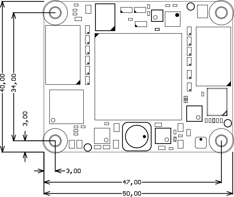
Mechanical Dimensions
GigaBee XC6SLX can reach a minimum vertical height of about 8 mm, if B2B connectors are not assembled. The maximum component height on the module board on the top side is about 3.5 mm. The maximum component height on the module board on the bottom side is about 3.0 mm.
...
GigaBee XC6SLX has 4 mounting holes, one in each corner. The module can be fixed by screwing M3 screws (ISO 262) onto a carrier board through those mounting holes.
Operating Temperature Ranges
Commercial grade: 0°C to +70°C.
...
The module operating temperature range depends also on customer design and cooling solution. Please contact us for options.
Weight
GigaBee XC6SLX weighs between 17.1 and 17.3 g with standard connectors.
Document Change History
Date | Revision | Contributors | Description | ||
|---|---|---|---|---|---|
| 2011-10-01 | 0.01 | AIK | Release. | ||
| 2011-10-05 | 0.02 | AIK | Added B2B pin-out section. | ||
| 2011-10-06 | 0.03 | AIK | Reformatted pin-out tables. Added eFUSE programming section. | ||
| 2011-10-06 | 0.04 | AIK | Added board photos. Additions to eFUSE section. | ||
| 2011-10-06 | 0.05 | AIK | Removed net length information for nets which can't be measured right. | ||
| 2011-10-06 | 0.06 | AIK | Added power consumption section. | ||
| 2011-10-08 | 0.07 | AIK | Little fixes after FDR audit. | ||
| 2011-10-12 | 0.08 | AIK | Fix in eFUSE section. | ||
| 2011-11-11 | 0.09 | AIK | Added pin numbering description for B2B connectors | ||
| 2012-01-20 | 0.10 | AIK | Added pin compatibility note and manual reference. | ||
| 2012-04-12 | 0.11 | AIK | Added FPGA banks VCCIO voltages table. | ||
| 2012-04-17 | 1.00 | FDR | Updated documentation link. Replaced obsolete ElDesI and RedMine links with current GitHub links. Updated dating convention. | ||
| 2012-05-18 | 1.01 | AIK | Corrected cross-reference in section 3.2. Corrected LED description. | ||
| 2012-06-18 | 1.02 | FDR | Removed junction temperature limits under connector current ratings. | ||
| 2012-07-18 | 1.03 | AIK | Added table with B2B signals summary per FPGA bank | ||
| 2012-10-30 | 2.01 | AIK | Fork to 01 and 02 board revisions | ||
| 2012-11-06 | 2.01 | AIK | Fixed bank 1 power options | ||
| 2012-11-21 | 2.02 | AIK | Updated module diagram | ||
| 2012-11-30 | 2.03 | AIK | Added Ethernet disable note | ||
| 2012-12-19 | 2.04 | AIK | Fixed SPI Flash size on block diagram | ||
| 2013-01-21 | 2.05 | AIK | Added PHY reset note | ||
| 2013-03-13 | 2.06 | AIK | Connectors current chapter moved to separate document | ||
| 2013-03-13 | 2.07 | AIK | Changed Bank 1 power supply description and VCCIO0 sources description | ||
| 2016-01-29 | 2.08 | AIK | Pause advertise correction | ||
| -21 | 2.02 | AIK | Updated module diagram | ||
| 2012-11-30 | 2.03 | AIK | Added Ethernet disable note | ||
| 2012-12-19 | 2.04 | AIK | Fixed SPI Flash size on block diagram | ||
| 2013-01-21 | 2.05 | AIK | Added PHY reset note | ||
| 2013-03-13 | 2.06 | AIK | Connectors current chapter moved to separate document | ||
| 2013-03-13 | 2.07 | AIK | Changed Bank 1 power supply description and VCCIO0 sources description | ||
| 2016-01-29 | 2.08 | AIK | Pause advertise correction | ||
| 2016-11-05 | 3.00 | FDR | Document ported to wiki and adapted to web presentation. | ||
| 2017-04-03 | TT | Added REV03 to assembly Variant Table | |||
| 2024-03-11 | 4.00 | MT | Added REV04 to assembly variant coding table | ||
| 2024-03-21 | 4.01 | VY | Updated SoM statuses in Assembly variants pin coding Table | 2016-11-05 | Document ported to wiki and adapted to web presentation.
Disclaimer
| Include Page | ||||
|---|---|---|---|---|
|
Overview
Content Tools