Page History
| Custom_table_size_100 |
|---|
| Page properties | ||||
|---|---|---|---|---|
| ||||
Template Revision 2.1 Design Name always "TE Series Name" + optional CPLD Name + "CPLD"
|
Overview
Firmware for PCB CPLD with designator U3: LCMX02-256HC
Feature Summary
- JTAG Multiplexer
- Module Power sequencing
- FPGA Configuration sequencing
- LED Status and User access
- FPGA IO User access
- I2C interface
Firmware Revision and supported PCB Revision
Product Specification
Port Description
| Name / opt. VHDL Name | Direction | Pin | Pullup/Down | Bank Power | Description | Note: PCB REV03 Connection | Note: PCB REV2 REV1 Connection |
|---|---|---|---|---|---|---|---|
| JTAGEN | in | 26 | --- | 3.3V | Switch JTAG between CPLD and FPGA (logical one for CPLD, logical zero for FPGA) | ||
| TMS / TMS | IN | 29 | DOWN | 3.3V | JTAG from B2B connector | ||
| TCK / TCK | IN | 30 | DOWN | 3.3V | JTAG from B2B connector | ||
| TDI / TDI | IN | 32 | DOWN | 3.3V | JTAG from B2B connector | ||
| TDO / TDO | OUT | 1 | DOWN | 3.3V | JTAG from B2B connector | ||
| F_TMS / F_TMS | OUT | 21 | DOWN | 3.3V | JTAG to FPGA | ||
| F_TCK / F_TCK | OUT | 17 | DOWN | 3.3V | JTAG to FPGA | ||
| F_TDI / F_TDI | OUT | 23 | DOWN | 3.3V | JTAG to FPGA | ||
| F_TDO / F_TDO | IN | 20 | DOWN | 3.3V | JTAG to FPGA | ||
| ULI_SYSTEM / ULI_SYSTEM | IN | 4 | UP | 3.3V | FPGA access W22 PIN / This pin is connected to internal clock of CPLD in CPLD firmware revision 1. / In CPLD firmware revision 2 is used as SCL pin of I2C interface between CPLD and FPGA. | ||
| FPGA_IO | INOUT | 10 | UP | 3.3V | FPGA access U22 PIN (PUDC) / This pin is connected to LED1 for CPLD firmware revision 1. / In CPLD firmware revision 2 and later is used as SDA pin of I2C interface between CPLD and FPGA after configuring the FPGA. | ||
| RESIN | IN | 16 | UP | 3.3V | RESETIN from B2B connector (Negative Reset) | ||
| DONE | IN | 28 | UP | 3.3V | FPGA Configuration DONE_0 Pin | ||
| PROG_B | OUT | 27 | UP | 3.3V | FPGA Configuration PROGRAM_B_0 Pin | ||
| PGOOD | OUT | 12 | UP | 3.3V | PGOOD to B2B connector | ||
| PG_ALL / PG_ALL | IN | 25 | UP | 3.3V | from module generated 3.3V Voltage | As PG_ALL renamed /In the hardware is connected to 3.3V./ In CPLD firmware is pulled up. | As PG_SENSE in CPLD firmware code. / In the hardware is connected to 3.3V. (Without label) |
| EN1 | IN | 11 | UP | 3.3V | Power Enable from B2B Connector (Positive Enable) | ||
| SYSLED2 / SYSLED1 | OUT | 8 | NONE | 3.3V | Module LED D2 (Red) | ||
| SYSLED1/ SYSLED2 | OUT | 9 | NONE | 3.3V | Module LED D1 (Green) | ||
| MODE | INOUT | 13 | UP | 3.3V | In firmware revision 1 is unused. / For firmware revision 2 is used as GPIO for user. | ||
| NOSEQ | INOUT | 14 | UP | 3.3V | In firmware revision 1 is unused. / For firmware revision 2 is used as GPIO for user. | ||
| ULI_CPLD / ULI_CPLD | INOUT | 5 | NONE | 3.3V | In firmware revision 1 is unused. / For firmware revision 2 is connected to internal clock of CPLD. |
Functional Description
JTAG
JTAG signals routed directly through the CPLD to FPGA. Access between CPLD and FPGA can be multiplexed via JTAGEN (logical one for CPLD, logical zero for FPGA).
Power
PGOOD is zero, if EN1 or PG_ALL is zero else high impedance state. PUDC is high during FPGA power upconfiguration.
FPGA Configuration
FPGA configuration process will be started, if RESIN, PG_ALL and EN1 is ONE.
I2C interface
CPLD firmware consists of a i2c t GPIO block. This subsystem provides i2c protocol interface to 32-bit (4 x 8-bit) (GPIO_input[31:0]) registers for reading from CPLD and (4 x 8-bit) (GPIO_output[31:0]) registers for writing in CPLD as general purpose parallel input and output (I/Os). The written and read data is communicated from/to FPGA via i2c bus interface protocol. The address of this block in the firmware is 0x20.In this case related i2c bus is bus 1.
| draw.io Diagram | ||||||||||||||||||||
|---|---|---|---|---|---|---|---|---|---|---|---|---|---|---|---|---|---|---|---|---|
|
| Register | Direction in CPLD | Address |
|---|---|---|
| GPIO_input[7:0] | Output (reading from CPLD) | 0x00 |
| GPIO_input[15:8] | Output (reading from CPLD) | 0x01 |
| GPIO_input[23:16] | Output (reading from CPLD) | 0x02 |
| GPIO_input[31:24] | Output (reading from CPLD) | 0x03 |
| GPIO_output[7:0] | Input (writing to CPLD) | 0x00 |
| GPIO_output[15:8] | Input (writing to CPLD) | 0x01 |
| GPIO_output[23:16] | Input (writing to CPLD) | 0x02 |
| GPIO_output[31:24] | Input (writing to CPLD) | 0x03 |
NOSEQ
Noseq pin can be used by user as GPIO. In this case the following table is valid:
| NOSEQ pin as output | Condition | Command in linux console |
|---|---|---|
| '1' | GPIO_output(16) = '0' | i2cset -y 1 0x20 0x02 0x00 |
| '0' | GPIO_output(16) = '1' | i2cset -y 1 0x20 0x02 0x01 |
| NOSEQ pin as input | Description | Command in linux console |
| Reading state of NOSEQ pin | GPIO_input(16) = NOSEQ | i2cget -y 1 0x20 0x02 |
MODE
Mode pin can read via I2C too:
| MODE pin | Description | Command in linux console |
|---|---|---|
| Reading state of MODE pin | GPIO_input(17) = MODE | i2cget -y 1 0x20 0x02 |
LED
| LED | STATUS | Condition | Description |
|---|---|---|---|
| SYSLED1 (Green) | Blink sequence ******** | RESIN = '0' | |
| SYSLED1 (Green) | Blink sequence ****oooo | DONE = '0' | |
| SYSLED1 (Green) | ON | GPIO_output(17) = '1' | Related command in linux console: i2cset -y 1 0x20 0x02 0x02 |
| SYSLED1 (Green) | OFF | otherwise | |
| LED | STATUS | Condition (User defined) | Description |
| SYSLED2 (Red) | OFF | MODE = '0' and NOSEQ = '0' | MODE can be changed for example for TE0703 carrier board via dip switch S2-4. |
| SYSLED2 (Red) | Blink sequence **oooooo | MODE = '0' and NOSEQ = '1' | NOSEQ can be set high via the following command in linux console:i2cset -y 1 0x20 0x02 0x00 |
| SYSLED2 (Red) | Blink sequence *****ooo | MODE = '1' and NOSEQ = '0' | MODE can be set high via setting MODE pin in carrier board. For example if you use TE0703 as carrier board MODE pin is connected with dip switch S2-4. |
| SYSLED2 (Red) | ON | MODE = '1' and NOSEQ = '1' |
Access to CPLD registers
CPLD registers can be accessed via i2c interface. In the following table is shown how these registers can be read or written:
| Register | Direction in CPLD | Address | Related instruction in linux console to access the register |
|---|---|---|---|
| GPIO_input[7:0] | Output (reading from CPLD) | 0x00 | i2cget -y 1 0x20 0x00 |
| GPIO_input[15:8] | Output (reading from CPLD) | 0x01 | i2cget -y 1 0x20 0x01 |
| GPIO_input[23:16] | Output (reading from CPLD) | 0x02 | i2cget -y 1 0x20 0x02 |
| GPIO_input[31:24] | Output (reading from CPLD) | 0x03 | i2cget -y 1 0x20 0x03 |
| GPIO_output[7:0] | Input (writing to CPLD) | 0x00 | i2cset -y 1 0x20 0x00 <data> |
| GPIO_output[15:8] | Input (writing to CPLD) | 0x01 | i2cset -y 1 0x20 0x01 <data> |
| GPIO_output[23:16] | Input (writing to CPLD) | 0x02 | i2cset -y 1 0x20 0x02 <data> |
| GPIO_output[31:24] | Input (writing to CPLD) | 0x03 | i2cset -y 1 0x20 0x03 <data> |
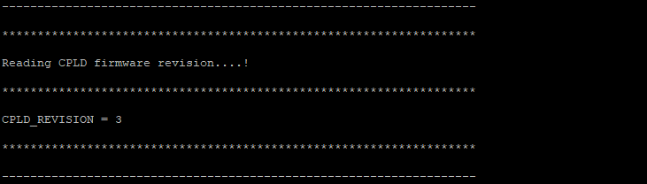
The first register GPIO_input[7:0] is used to show CPLD revision.
| Register | Address | Related data | Read/Write by user | Description |
|---|---|---|---|---|
| GPIO_input[7:0] | 0x00 | CPLD REVISION (8 bits) | No | |
| GPIO_input(16) | 0x02 | NOSEQ pin | Yes | To read NOSEQ pin : i2cget -y 1 0x20 0x02 --> Bit 0 shows NOSEQ pin state. |
| GPIO_input(17) | 0x02 | MODE pin | Yes | To read MODE pin : i2cget -y 1 0x20 0x02 --> Bit 1 shows MODE pin state. |
| Register | Address | related data | Description | |
| GPIO_output(16) | 0x02 | NOSEQ pin | Yes | For example to set NOSEQ pin high: i2cset -y 1 0x20 0x02 0x00 |
| GPIO_output(17) | 0x02 | SYSLED1 (Green) | Yes | To turn SYSLED1 (Green) on : i2cset -y 1 0x20 0x02 0x02 |
The CPLD revision is displayed in linux console while booting as shown:
| Scroll Title | ||||
|---|---|---|---|---|
| ||||
|
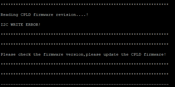
If CPLD firmware is older than REV02, then CPLD revision will not be displayed and user should update the firmware. In this case the following message will be displayed:
| Scroll Title | ||||
|---|---|---|---|---|
| ||||
|
Appx. A: Change History
Revision Changes
REV02 to REV03 changes:
- The state of FPGA_IO pin (PUDC pin) is set to high to measure the voltage of the FPGA IO pins correctly even if the FPGA is not programmed.
REV01 to REV02 changes:
Renaming the port signals according to the schematic.
Defining and reading CPLD Revision via i2c interface.
JTAG signal timing adjustment
Adding i2c to gpio ip (i2c_slave.vhd)
LEDs functions was changed:
SYSLED1 (green LED) shows the DONE and RESIN and GPIO_output(17) bit state of GPIO_output register.
SYSLED2 (Red LED) shows the state of NOSEQ and MODE pins.
- PG_SENSE renamed to PG_ALL.
- PGOOD pulled up.
Document Change History
To get content of older revision got to "Change History" of this page and select older document revision number.
| Page properties | ||||
|---|---|---|---|---|
| ||||
|
| Date | Document Revision | CPLD Firmware Revision | Supported PCB Revision | Authors | Description | ||||||||||||||||||||||
|---|---|---|---|---|---|---|---|---|---|---|---|---|---|---|---|---|---|---|---|---|---|---|---|---|---|---|---|
|
| REV03 | REV01, REV02, REV03 | |
| ||||||||||||||||||||||
| 2022-10-20 | v.25 | REV02 | REV01, REV02, REV03 | Mohsen Chamanbaz |
| ||||||||||||||||||||||
| 2018-05-15 | v.24 | REV01 | REV01, REV02 | John Hartfiel |
| ||||||||||||||||||||||
| 2017-01-26 | v.17 | REV01 | REV01, REV02 |
| |||||||||||||||||||||||
| 2016-11-04 | v.1 | --- |
|
| |||||||||||||||||||||||
| All |
|
Appx. B: Legal Notices
| Include Page | ||||
|---|---|---|---|---|
|
| Scroll Only | ||
|---|---|---|
|
| Scroll pdf ignore | ||||||
|---|---|---|---|---|---|---|
|
Overview
Content Tools