Page History
...
| Scroll pdf ignore | ||||
|---|---|---|---|---|
Table of Contents
|
Overview
| Scroll Only (inline) |
|---|
Online version of this manual and other related documents can be found at https://wiki.trenz-electronic.de/display/PD/TE0701 |
...
See page "4 x 5 cm carriers" to get information about the SoMs supported by the TE0701 Carrier Board.
Main Components
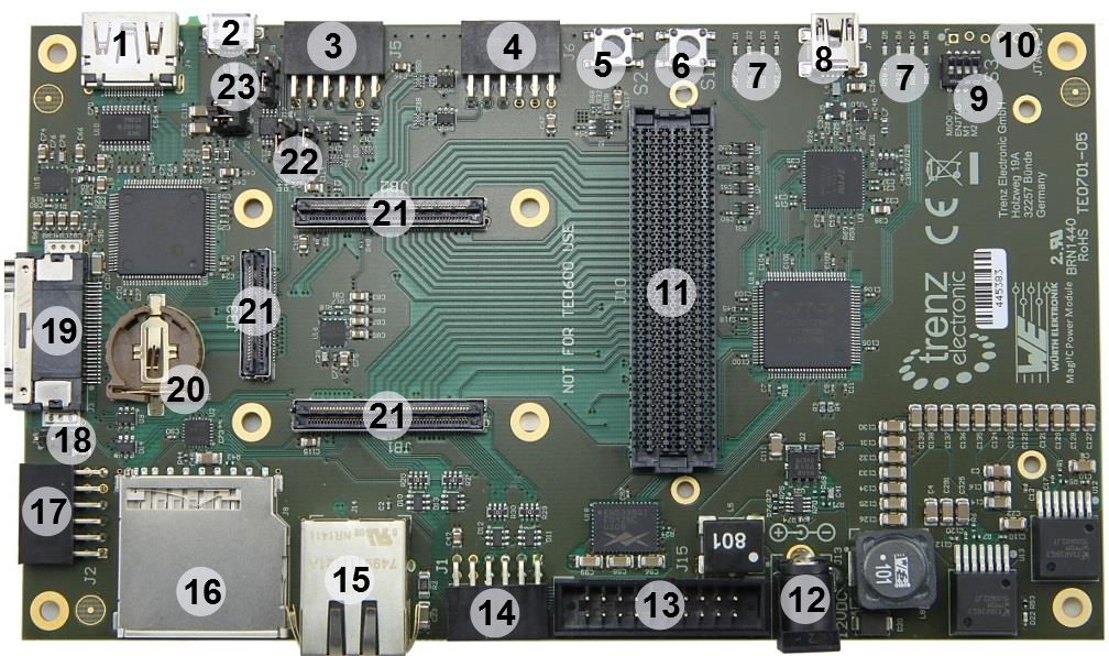
Figure 1: 4x5 SoM carrier board TE0701-05
...
- HDMI Connector (1.4 HEAC Support)
- Micro USB Connector (Device, Host or OTG Modes)
Pmod Connector for Zynq-module PL (4 LVDS-pairs, max. VCCIO-Voltage 3,3V)
- Pmod Connector for Zynq-module PL (4 LVDS-pairs, max. VCCIO-Voltage FMC_VADJ)
- User Push Button S2 ("RESTART" button by default)
- User Push Button S1 ("RESET" button by default)
- User LEDs (function mapping depends on firmware of System-Controller-CPLD)
- Mini USB Connector (USB JTAG and UART Interface)
- User 4-bit DIP Switch
- Direct access to System-Controller-CPLD JTAG-Interface (Solder Pads, pin-strip need to be mounted)
- VITA 57.1 compliant FMC LPC Connector with digitally programmable FMC VADJ Power Supply
- Barrel jack for 12V Power Supply
- ARM JTAG Connector (DS-5 D-Stream) - PJTAG to EMIO multiplexing needed
- Pmod Connector (J1, 3.3V): mapped to 8 Zynq PS MIO0-bank-pins (MIO0, MIO9 to MIO15) when using TE0720 (same mapping as on Zedboard), 6 pins (MIO10 to MIO15) are additionally connected to TE0701 CPLD Carrier Controller
- RJ45 GbE Connector
- SD Card Connector - Zynq SDIO0 Bootable SD port
- Pmod Connector (J2, 3.3V): 6 pins (PX0 to PX5) can be multiplexed by Texas Instruments TXS02612RTWR SDIO Port Expander to SD Card pins (MIO1 bank when using TE0720), 2 pins are connected to TE0701 System-Controller-CPLD (PX6 and PX7)
- Jumper J18
- Mini CameraLink Connector
- Battery holder for CR1220 (RTC backup voltage)
- Trenz 4x5 module Socket (3x Samtec LSHM Series Connectors)
- Jumper J17, J21
- Jumper J9, J19, J20
Key Features
- Overvoltage-, undervoltage- and reversed- supply-voltage-protection
- Barrel jack for 12V power suppy
- Carrier Board System-Controller-CPLD Lattice MachXO2 1200HC, programable by Mini-USB JTAG-Interface J7
- JTAG-Interface of System-Controller-CPLD directly accessible by additional connector J23, pin strip has to be mounted on existing solder pads
- Zynq-module programable by ARM-JTAG-Interface-Connector (J15) or by System-Controller-CPLD via Mini-USB JTAG-Interface J7 or JTAG-Interface on FMC-Connector J10
- Mini CameraLink
- RJ45 Gigabit Ethernet Jack with 2 integrated LEDs.
- FPGA Mezzanine Card (FMC) Connector J10 for acces to Zynq-Module's LVDS-pairs, operable with adjustable IO-voltage FMC_VADJ
- USB JTAG- and UART-Interface (FTDI FT2232HQ) with Mini-USB-Connector J7
- ADV7511 HDMI Transmitter with HDMI-Connector J4
- 8 x user LEDs routed to System-Controller-CPLD, 8 x red
- 2 x user-push button routed to System-Controller-CPLD; by default configured as system "RESET" and "RESTART" button (depends on CPLD-Firmware)
- 4-bit DIP-Switch for base-board-configuration, 3 switches routed to System-Controller-CPLD, 1 switch routed to Zynq-module (MIO0)
- PMOD-Connectors to access Zynq-Module's LVDS-pairs and MIO-Pins
- Micro SD card socket, can be used to boot system
- Zynq-Module-SDIO-Port also accessible by PMOD-Connector J2 via SDIO Port Expander
- Micro-USB-Interface (J12) connected to Zynq-module (Device, Host or OTG modes)
- Trenz 4x5 module Socket (3 x Samtec LSHM series connectors)
Interfaces and Pins
Board to Board (B2B) I/O's
For detailed information about the B2B pin out, please refer to the Master Pinout Table.
Micro SD Card Socket
Micro SD Card socket is not directly wired to the B2B connector pins, but through a Texas Instruments TXS02612 SDIO Port Expander, which is needed for voltage translation due to the different voltage levels of the Micro SD Card and MIO bank 501 of the Xilinx Zynq-module. The Micro SD Card has 3.3V signalling, but the MIO Bank 501 on the Xilinx Zynq-module chip is set to 1.8V.
The Micro SD Card Socket is also accessible by PMOD-Connector J2, which is configurible by the "SEL_SD"-signal of the System-Controller-CPLD
Dual channel USB to UART/FIFO
The TE0701 has on-board USB 2.0 High Speed to UART/FIFO IC FT2232HQ from FTDI. Channel A can be used as JTAG-Interface (MPSSE) to program the System-Controller-CPLD, Channel B can be used as UART-Interface routed to CPLD. There also 4 additionally bus-lanes available for user-specific use. The FT2232HQ-Chip can also be used as FIFO-Buffer.
There is also a standard 256 Byte EEPROM connected to the FT2232HQ-chip available to store custom configuration settings. EEPROM settings can be changed using FTDI provided tools that can be downloaded from FTDI website. See FTDI website for more information.
USB Interface
TE0701 board has two physical USB-connectors:
- J7 as mini-USB-connector wired to on-board FTDI FT2232HQ chip.
- J12 as micro-USB-connector wired to B2B connector JB3 (there is usually an USB-transceiver on the SoMs).
JTAG Interface
JTAG access to the CPLD and Xilinx Zynq-module is provided via Mini-USB JTAG Interface (FTDI FT2232H) and controlled by DIP switch S3.
The JTAG port of the CPLD is enabled by setting switch S3 labeled as "ENJTAG" to the OFF-position.
LED's
There are eight LED's (L1 to L8) available to the user. All LEDs are red colored and connected to the on-board System-Controller-CPLD. Their functions are programmable and depend on the firmware of the System-Controller-CPLD. For detailed information, please refer to the documentation of the TE0701 Sytem-Controller-CPLD.
...
One green LED D22 shows the avaibility of the 3.3V supply voltage of the TE0701 Carrier Board.
4-bit DIP-switch
Additionally, on the TE0701 Carrier Board there is a 4-bit DIP-switch (S3; see (9) in Figure 1) available. The default S3 switch mapping is as follows:
| S3-1 | CM1: Mode pin 1 (routed to Carrier Controller) |
| S3-2 | CM0: Mode pin 0 (routed to Carrier Controller) |
| S3-3 | JTAGEN: Set to ON for normal JTAG operation. Must be moved to OFF position for TE0701 CPLD update only |
| S3-4 | MIO0: Readable signal by Carrier Controller and TE07xx Module |
User-Push-Buttons
On the TE0701 Carrier Board there are two push buttons (S1 and S2) and are available to the user. The default PB mapping is as follows:
| Name | Default Mapping: | ||
|---|---|---|---|
| S1 | If S1 is pushed, the active-low RESet IN (RESIN) signal will be asserted. Note: This reset can also be forced by the FTDI USB-to-JTAG interface. | ||
| S2 | If S2 is pushed, the active-high Power ON (PON) signal (that is internally pulled-up) will be deasserted, which can be considered as a "RESTART" button to switch off (push button) and on (release button) all on-module power supplies (except 3.3VIN). Note: The capability to be enabled the first time will become active shortly after Power on Reset (POR).
|
Ethernet
TE0701 has a RJ45 Gigabit Ethernet MAGJACK (J14) with two LED's.
...
With initial Carrier Controller design, one RJ45 LED (the right one) is connected to module NOSEQ pin that functions as PHY LED output on TE0720 with default settings. The other LED is connected to a pin of the I2C-to-GPIO-module and can be controlled by the control register of this module on the Systen-Controller-CPLD if desired.
Pmod Slots
J5 and J6 Pmod signal routing is done as differential pairs for pins 1-2, 3-4, 7-8, 9-10
Please use Master Pinout Table table as primary reference for the pin mapping information.
Power
Power Supply
Power supply with minimum current capability of 3A at 12V for system startup is recommended.
TE0701 jumper and DIP switch overview
On the TE0701 carrier boards (TE0701-03 and higher revisions) different hardware/software configurations can be chosen by 6 jumpers and one 4-bit DIP switch:
...
The purpose of the jumpers and the DIP switch of the Carrier Board will be explained in the following sections.
Configuring VCCIO-Voltage
The Zynq-module power supply is fixed to 5V!
...
M1 | M2 | FMC_VADJ Value |
|---|---|---|
| OFF | OFF | 1.8V |
| OFF | ON | 2.5V |
| ON | OFF | 3.3V |
| ON | ON | I2C Controlled |
Table 3: Switch S3 positions for fixed values of the FMC_VADJ voltage
Configuring 12V Power Supply Pin on the CameraLink Connector
Finally, a 12V power supply can be connected to pin 26 of the CameraLink by closing J18. However, this option is disabled by default (J18: OPEN).
Configuring Power Supply of the Micro USB Connector (Device, Host or OTG Modes)
The TE0701 carrier board can be configured as a USB host. Hence, it must provide from 5.25V to 4.75V to the board side of the downstream connection (micro USB port on J12; 13). To provide sufficient power, a TPS2051 power distribution switch is located on the carrier board in between the 5V power supply and the Vbus signal of the USB downstream port interface. If the output load exceeds the current-limit threshold, the TPS2051 limits the output current and pulls the overcurrent logic output (OC_n) low, which is routed to the on-board CPLD. The TPS2051 is put into operation by setting J19 CLOSED. J20 provides an extra 100µF decoupling capacitor (in addition to 10µF) to further stabilize the output signal. Moreover, a series terminating resistor of either 1K (J9: 1-2, 3) or 10K (J9: 1, 2-3) is selectable on the "USB-VBUS" signal. Both signals, USB-VBUS and VBUS_V_EN (that enables the TPS2051 on "high") are routed (as well as the corresponding D+/- data lines) via the on-board connector directly to the USB 2.0 high-speed transceiver PHY from SMSC (USB3320) on the GigaZee module, which is, in turn, connected to the Zynq FPGA. In summary, the default jumper settings are the following: J9: 1-2, 3 (1K series terminating resistor); J19: CLOSED (TPS2051 in operation); J20: CLOSED (100 µF added).
Additionally, the TE0701 carrier board is equipped with a second mini USB port (J7; see (8) in Figure 1) that is connected to a "USB to multi-purpose UART/FIFO IC" from FTDI (FT2232HQ) and provides a USB-to-JTAG interface between a host PC and the TE0701 carrier board and the Zynq-module, respectively. Because it acts as a USB function device, no power switch is required (and only a ESD protection must be provided) in this case.
Power On Reset (POR)
On the TE0701 the 5.0V and 3.3V power supply rails are generated by high performance DC-DC Enpirion -converters (EN2340QI) from the external 12V supply. While the 3.3V plane supplies several on-board components (e.g., Lattice CPLD and FTDI Dual USB UART/FIFO IC), the 5V plane is mainly provided for power supply of the module to be carried (e.g., TE0720 Zynq SoC module). For the latter, however, special considerations must be taken (see TE0720 Power Supply). Therefore, the on-module system controller (SC) must be provided with information about the power-on-reset (POR) process, namely, the following control signals EN1, RESIN, and NOSEQ. And the SC provides, in turn, the status signal PGOOD down to the on-board CPLD.
...
| Info |
|---|
| For more information on the preceding signals please consult the corresponding Wiki documentation of the TE0720 System Management Controller. |
Technical Specifications
Absolute Maximum Ratings
| Parameter | Min | Max | Units | Notes |
|---|---|---|---|---|
Vin supply voltage | 11.4 | 12.6 | V | ANSI/VITA 57.1 FPGA Mezzazine Card (FMC) Standard |
Storage Temperature | -55 | 125 | °C | - |
Recommended Operating Conditions
| Parameter | Min | Max | Units | NotesReference document | |
|---|---|---|---|---|---|
| Vin supply voltage | 11.4 | 12.6 | V | - |
Physical Dimensions
Board size: PCB 170.4 mm × 98 mm. Notice that some parts the are hanging slightly over the edge of the PCB like the mini USB-jacks (ca. 1.4 mm), the ethernet RJ-45 jack (ca 2.2 mm) and the mini CameraLink connector (ca. 7 mm), which determine the total phycial demensions of the carrier board. Please download the assembly diagram for exact numbers.
Mating height of the module with standard connectors: 8mm
PCB thickness: ca. 1.65mm
Highest part on the PCB is the ethernet RJ-45 jack, which has an approximately 17 mm overall hight. Please download the step model for exact numbers.
...
Figure 3: Physical Dimensions of the TE0701 carrier board
Operating Temperature Ranges
Commercial grade: 0°C to +70°C.
Board operating temperature range depends also on customer design and cooling solution. Please contact us for options.
Weight
ca. 188 g - Plain board
Document Change History
| date | revision | authors | description |
|---|---|---|---|
| 2016-11-28 | Ali Naseri | TRM adjustment to the newest revision (05) of TE0701 Carrier Board | |
| 2014-02-18 | 0.2
| Sven-Ole Voigt | TE0701-03 (REV3) updated |
| 2014-01-05 | 0.1 | Sven-Ole Voigt | Initial release |
All |
Hardware Revision History
| Date | Revision | Notes | PCN | Documentation link |
|---|---|---|---|---|
| - | 01 | Prototype | ||
| - | 02 | Prototype | ||
| - | 03 | changed DC/DC converters | ||
| - | 04 | |||
| - | 05 | improved manufacturing |
...
Hardware revision number is printed on the PCB board next to the module model number separated by the dash.
Disclaimer
| Include Page | ||||
|---|---|---|---|---|
|
...
Overview
Content Tools