Page History
...
The TE0710 is equipped with two Sitara reference clocks MEMS oscillators to provide clock signals to the Ethernet PHYs and for the two on board 512 MByte DDR3 SRRAM-board Ethernet PHY's and DDR3 SDRAM.
| Clock | Frequency | IC | Connected to | Notes |
|---|---|---|---|---|
Reference oscillator clock for USB to UART/FIFO Bridge (FT2232H) | 12 MHz | U9 SiT8008AI-73-XXS-12.000000E | IC U6, FTDI FT2232H | - |
| FPGA bank 14 reference clock input | 100 MHz | U8 SiT8008AI-73-XXS-100.000000E | FPGA bank 14, pin P17 | reference clock for general user purposes |
...
The system controller is used to coordinate the configuration of the FPGA. The FPGA is held in reset (by driving the PROG_B signal) until the power supplies have sequenced. Low level at NRST_SC0 pin also resets the FPGA. This signal can be driven from the user’s PCB via the B2B connector pin JM2-18. Input EN_SC3 is also gated to FPGA Reset and should be open or pulled up for normal operation. EN_SC3 low turns off on board DCDC DC-DC converters and stops power-on sequencing.
...
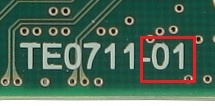
Hardware revision number is printed on the PCB board together with the module model number separated by the dash.
Document Change History
| Date | Revision | Contributors | Description | |
|---|---|---|---|---|
| 20162017-1201-2001 | Ali Naseri | TRM revision | ||
| 2015-06-05 | 0.1 |
| initial version |
Disclaimer
...
Overview
Content Tools