Page History
...
Figure 2: TE0741 (REV 02).
- Xilinx Kintex-7 FPGA (Kintex-7)
- EN63A0QI Voltage Regulator 1.0V (Slave)
- EN63A0QI Voltage Regulator 1.0V (Master)
- programmable PLL - clock generator (Si5338)
- B2B connector JM1 (0,50 mm Razor Beam™ High Speed Hermaphroditic Terminal/Socket Strip (LSHM-150))
- B2B connector JM3 (0,50 mm Razor Beam™ High Speed Hermaphroditic Terminal/Socket Strip (LSHM-150130))
- B2B connector JM2 (0,50 mm Razor Beam™ High Speed Hermaphroditic Terminal/Socket Strip (LSHM-150))
- System Controller CPLD (Lattice LCMXO2-256HC): 256 Macrocell CPLD
- 32 Mbyte -MByte Quad SPI Flash memory
- EP53F8QI Voltage Regulator 1.8V
- EP53F8QI Voltage Regulator 1.0V MGTAVCC
- EP53F8QI Voltage Regulator 1.2V MGTAVTT
- TPS27082L load switch for 3.3V voltage level
...
- Industrial-grade Xilinx Kintex-7 FPGA module (70T*, 160T*, 325T, 410T)
* Device supported by the free Xilinx Vivado WebPACK software. - 256-Mbit (32-MByte) Quad SPI Flash memory (for configuration and operation) accessible through:
- FPGA
- JTAG port (SPI indirect (Bus Width width x4))
- 8 GTX transceivers
- FPGA configuration through:
- JTAG (B2B connector)
- SPI Flash memory
- 25 MHz low jitter oscillator with shutdown control
- Programmable quad PLL - clock generator
- On-board high-efficiency DC-DC converters
- GTX voltage regulators with control enable
- Core voltage regulator: 20A (2 x Enpirion DC/DC regulators with load-sharing)
- Supply voltages: either 3.3V or 3.3V and 5V
- Plug-on module with two 100-pin and one 60-pin high-speed hermaphroditic stacking strips
- Up to 144 (94 for 70T) FPGA I/O pins available on B2B strips (up to 65 LVDS pairs possible)
- 2 user LED's, 1 DONE FPGA pin LED, 1 System Controller status LED
- System management and power sequencing
- AES bit-stream encryption
- eFUSE bit-stream encryption
- Evenly spread supply pins for good signal integrity
- Assembly options for cost or performance optimization available on request
...
I/O signals connected to the FPGA's FPGAs I/O banks and B2B connector:
| Bank | Type | B2B Connector | I/O Signal Count | Voltage | Notes |
|---|---|---|---|---|---|
0 | HR | - | - | 3.3V | Configuration bank |
12 | HR | JM2 | 50 I/ |
Os, 24 LVDS |
pairs |
User | HR-Banks support voltages from 1.2V to 3.3V standards. NOTE: BANK 12 IS NOT AVAILABLE ON THE K70T DEVICE. | ||
13 | HR | JM1 | 48 I/ |
Os, 24 LVDS |
pairs |
User | HR-Banks support voltages from 1.2V to 3.3V standards. | |
14 | HR | JM1 |
JM3 | 8 I/ |
Os 4 I/ |
Os, 2 LVDS |
pairs |
3.3V | pins at B2B connector JM1, 3.3V IO-voltage. | ||
15 | HR | JM2 | 18 I/ |
Os, 9 LVDS |
pairs |
User | HR-Banks support voltages from 1.2V to 3.3V standards. | ||
16 | HR | JM3 | 16 I/ |
Os, 8 LVDS |
pairs |
User | HR-Banks support voltages from 1.2V to 3.3V standards. | ||||
32 | HP | NC | - | - | Bank not used. |
33 | HP | NC | - | - | Bank not used. |
| 34 | HP | NC | - | - | Bank not used. |
Table 2: Voltage ranges and pin-outs of available logic banks of the FPGA.
...
JTAG access to the Xilinx Kintex7 and to the System Controller CPLD is provided through B2B connector JM2.
| JTAG Signal | B2B Connector |
|---|---|
| TCKTMS | JM2-9993 |
| TDI | JM2-95 |
| TDO | JM2-97 |
| TMSTCK | JM2-9399 |
Table 3: Pin-mapping of JTAG Interface on B2B connector.
| Note |
|---|
| Select by JTAGMODE pin on B2B connector JM1-89 either to access FPGA Artix7 (JTAGMODE pin driven low or open) or System Controller via JTAG (JTAGMODE pin driven high). |
...
| Pin Name | Mode | Function | Default Configuration | B2B Connector |
|---|---|---|---|---|
| PGOOD | Output | Power Good | Active high when all on-module power supplies are working properly. | JM1-30 |
| RESIN | Input | Reset | Active low reset signal, drive low to keep the system in reset (FPGA pin PROG_B will be driven by CPLD). | JM2-18 |
| JTAGMODE | Input | JTAG Select | Low for normal operation, high (3.3V) to programm program the System Controller CPLD. | JM1-89 |
Table 4: Pin-description of System Controller CPLD.
LED's
There are four LED's available on TE0741 SoM. Two status LED's (D3 and D4) and two user configurable LED's (D1 and D2).
| LED | Color | Connected to | Description and Notes |
|---|---|---|---|
| D1 | greenGreen | LED2 | User configurable LED. |
| D2 | redRed | LED1 | User configurable LED. |
| D3 | greenGreen | DONE | Reflects inverted DONE signal, ON when FPGA is not configured, OFF as soon as PL is configured. This LED will not operate if the the 3.3V power rail is not available. After FPGA configuration the user can use USRACCESSE2 to control Done LED. |
| D4 | greenGreen | C_LED | Connected to the system controller indicating status of the module: Steadily lit: RESIN pin is kept low. Blinking fast (0.1s on/off): Power sequencing fault (PG_ALL = 0). Blinking at medium speed (0.5s on/off): Power sequencing has completed but the FPGA is not configured (PG_ALL = 1, DONE = 0). Blinking slow (1s on/off): FPGA is configured and board is ready (PG_ALL = 1, DONE = 1). It is also possible to program the System Controller CPLD to connect this LED to FPGA pin named XIO. |
...
| Clock | Frequency | IC | FPGA | Notes |
|---|---|---|---|---|
PLL reference | 25 MHz | U3 SiT8208AI | - | Activated by CLK_EN pin of FPGA. |
GTX REFCLK0 | - | B2B | D5/D6 | B2B connector pins: MGT_CLK_0_N: JM3-31 MGT_CLK_0_P: JM3-33 Needs decoupling and differential terminator on base board. |
| GTX GTX REFCLK1 | 125 MHz | U2 Si5338 | F5/F6 | PLL clock 1, default frequency is 125 MHz. |
| GTX GTX REFCLK2 | - | B2B | H5/H6 | B2B connector pins: MGT_CLK_2_N: JM3-32 MGT_CLK_2_P: JM3-34 Needs decoupling and differential terminator on base board. |
| GTX GTX REFCLK3 | 125 MHz | U2 Si5338 | K5/K6 | PLL clock 2, default clock is 125 MHz. |
| Bank 14 input clock | 100 MHz | U2 Si5338 | F22/E23 | PLL clock 0, default frequency is 100 MHz. |
Table 6: Clocks overview.
...
On-board Peripherals
Programmable PLL Clock (Phase-Locked Loop)
...
Table 8: Maximum current of power supplies supplies .
* TBD - To Be Determined soon with reference design setup.
...
Figure 6: Connections between the on-board DCDC DC-DC and LDO regulators.
Power Rails
...
| Bank | Schematic Name | Voltage | Range |
|---|---|---|---|
| 0 Config | 3.3V | 3.3V | - |
| 12 | VCCIO12 | user | HR: 1.2V to 3.3V |
| 13 | VCCIO13 | user | HR: 1.2V to 3.3V |
| 14 | 3.3V | 3.3V | - |
| 15 | VCCIO15 | user | HR: 1.2V to 3.3V |
| 16 | VCCIO16 | user | HR: 1.2V to 3.3V |
Table 10: Range of FPGA's FPGAs bank voltages.
See the Kintex-7 datasheet (DS182) for the allowable voltage range.
...
Recommended Operation Conditions
| Parameter | Min | Max | Units | Notes | Reference Document |
|---|---|---|---|---|---|
| VIN supply voltage | 2.4 | 5.5 | V | - | EP53F8QI data sheet |
| 3.3VIN supply voltage | 3.135 | 3.465 | V | 3,3V ± 5% | - |
| PL I/O bank supply voltage for HR I/O banks (VCCO) | 1.14 | 3.465 | V | - | Xilinx datasheet DS182 |
| I/O input voltage for HR I/O Banks | - 0.20 | VCCO+0.2 | V | - | Xilinx datasheet DS182 |
| GT receiver (RXP/RXN) and transmitter (TXP/TXN) | (*) | (*) | - | - | * check datasheet DS182 |
| Voltage on Module JTAG pins | 3.135 | 3.465 | V | - | - |
Table 13: Recommended operation conditions.
...
All dimensions are shown in mmmillimeters.
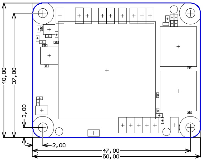
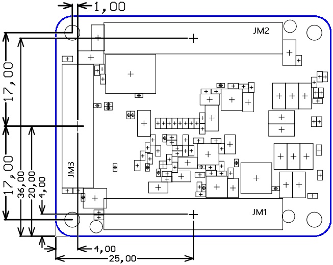

Figure 7: Physical Dimensions of the TE0741-02 board.
...
Hardware Revision History
| Date | Revision | Notes | PCN | Documentation |
|---|
| 2013-11-06 | 02 |
| TE0741 | |
| 01 | First production release |
Hardware revision number is printed written on the PCB board together with the module model number separated by the dash.
...
| Date | Revision | Contributors | Description | ||||
|---|---|---|---|---|---|---|---|
| 2017-01-12 | John Hartfiel | Correction: B2B and FPGA Bank location | |||||
| 2016-12-14 | 19 | Ali Naseri | TRM revision | ||||
| 2013-12-02 | 0.1 | initial Initial version |
Disclaimer
| Include Page | ||||
|---|---|---|---|---|
|
...
Overview
Content Tools