Page History
...
Figure 1: TE0741 Block Diagram.
Main Components
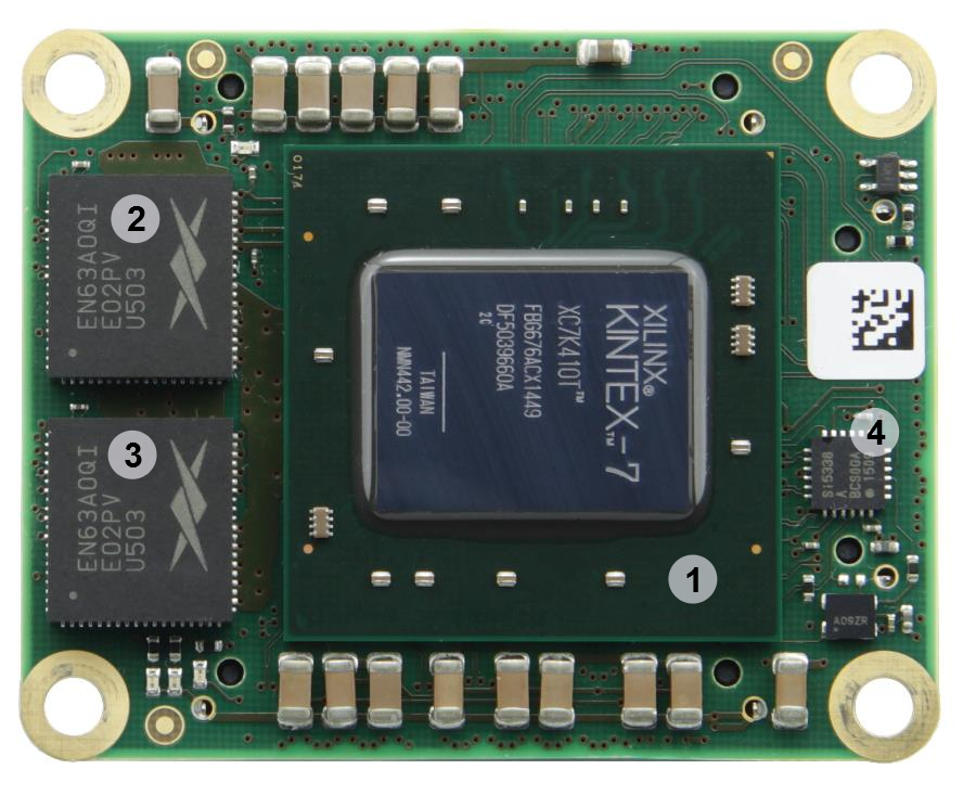
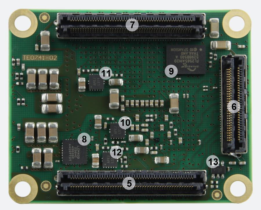
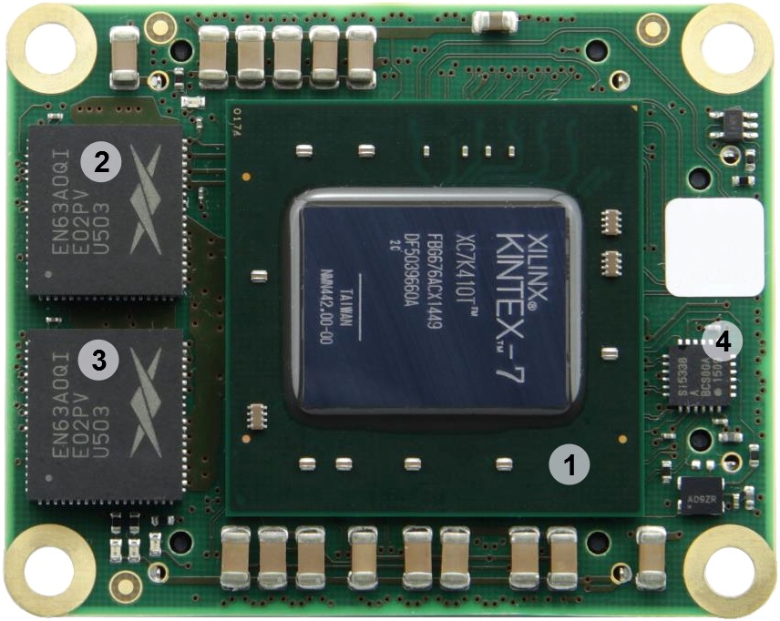
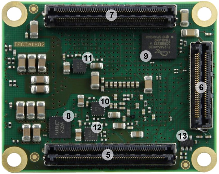
Figure 2: TE0741 (REV 02).
...
There are four LED's available on TE0741 SoM. Two status LED's (D3 and D4) and two user configurable LED's (D1 and D2).
| LED | Color | Connected to | Description and Notes |
|---|---|---|---|
| D1 | Green | LED2 | User configurable LED. |
| D2 | Red | LED1 | User configurable LED. |
| D3 | Green | DONE | Reflects inverted DONE signal, ON when FPGA is not configured, OFF as soon as PL is configured. This LED will not operate if the the 3.3V power rail is not available. After FPGA configuration the user can use USRACCESSE2 to control Done LED. |
| D4 | Green | C_LED | Connected to the system controller indicating status of the module: Steadily lit: RESIN pin is kept low. Blinking fast (0.1s on/off): Power sequencing fault (PG_ALL = 0). Blinking at medium speed (0.5s on/off): Power sequencing has completed but the FPGA is not configured (PG_ALL = 1, DONE = 0). Blinking slow (1s on/off): FPGA is configured and board is ready (PG_ALL = 1, DONE = 1). It is also possible to program the System Controller CPLD to connect this LED to FPGA pin named XIO. |
Table 5: Description of the on board LED's.
...
Table 10: Range of FPGAs bank voltages.
See the Xilinx Kintex-7 datasheet (DS182) for the allowable voltage rangeranges allowed.
Board to Board Connectors
...
- Module size: 50 mm × 40 mm
- Mating height with standard connectors: 8mm
- PCB thickness: 1.6mm
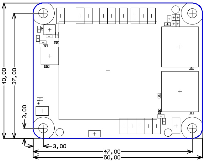
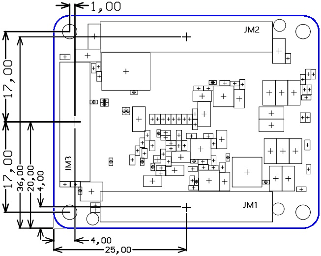
Figure 7: Physical dimensions of the TE0741-02 module. All dimensions are shown in millimeters.
...
Hardware Revision History
| Date | Revision | Notes | PCN | Documentation |
|---|---|---|---|---|
| 2013-11-06 | 02 |
|
|
| TE0741 | |||
| 01 | First production release |
Hardware revision number is written on the PCB board together with the module model number separated by the dash.

Document Change History
| Date | Revision | Contributors | Description |
|---|---|---|---|
| 2017-01-13 | V40 | New product images and physical dimension drawings. Formatting improvements and small corrections. | |
| 2017-01-12 | Correction: B2B and FPGA Bank location. | ||
| 2016-12-14 | 19 | TRM revision. | |
| 2013-12-02 | 0.1 | Initial version. |
Disclaimer
| Include Page | ||||
|---|---|---|---|---|
|
...
Overview
Content Tools