Page History
| Scroll Ignore |
|---|
Download PDF Version version of this Documentdocument. |
| Scroll pdf ignore | ||||
|---|---|---|---|---|
Table of Contents
|
Overview
...
The Trenz Electronic TE0705 Carrier Board is a base-board for 4x5 SoMs, which exposes the MIO- and the PS/PL-pins of the SoM to accessible connectors and provides a whole range of on-board components to test and evaluate Trenz Electronic 4x5 SoMs.carrier board provides functionality for testing, evaluation and development purposes of company's 4 x 5 cm SoMs (System on Module). The carrier board is equipped with a broad range of various components and connectors for different configuration setups and needs. On-module functional components and multipurpose I/Os of the SoM's PL and PS logic are connected via board-to-board connectors to the carrier board components and connectors for easy user access.
See See page "4 x 5 cm carriers" to get page for more information about the SoMs supported by the TE0705 Carrier Board.
Block Diagram
supported 4 x 5 cm SoMs.
| Scroll Only (inline) |
|---|
Refer to http://trenz.org/te0720-info for the current online version of this manual and other available documentation.
|
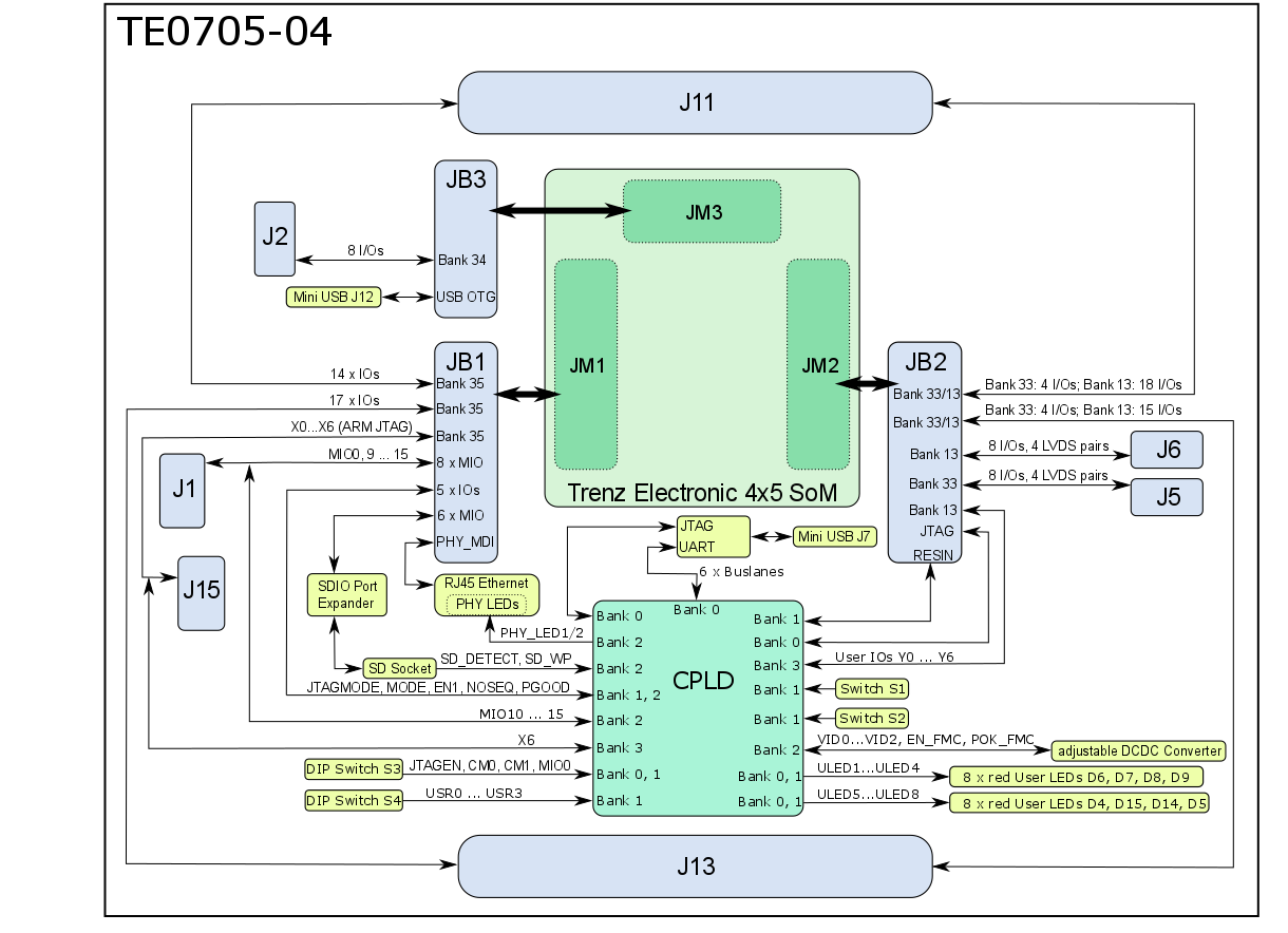
Block Diagram
Figure 1Figure 1: TE0705-04 Block Diagram.
Main Components
Figure 2: 4x5 4 x 5 SoM carrier board TE0705-04.
TE0705-04:
- ARM JTAG Connector (DS-5 D-Stream) J15 - PJTAG to EMIO multiplexing neededfunctionality depends on connected module
- 12-pin IDC Molex 90130-3212 header socket J1 (right angle, max. VCCIO - voltage : 3.3V): mapped to 8 Zynq PS MIO0-bank-pins (MIO0, MIO9 to MIO15), 6 pins (MIO10 to MIO15) are additionally connected to TE0705 System-Controller-CPLD
RJ45 GbE Connector
- SD Card Socket - Zynq SDIO0 Bootable bootable SD port
- 12-pin IDC Molex 90130-3212 header socket (right angle) J2 for access to Zynq-module's PL IO-bank pins (not usable as LVDS-pairs, only single-ended IOs, max. VCCIO-voltage: VIOTB)J2
- Micro USB Connector J12 (Micro USB Connector J12 (Device, Host or OTG Modes)
- Battery holder for CR1220 (RTC backup voltage)
- 12-pin IDC Molex 90130-1212 header socket (vertical) J5 for access to Zynq-module's PL IO-bank pins (4 LVDS-pairs, max. VCCIO-voltage: VIOTB)
- 12-pin IDC header socket (vertical) J6 for access to Zynq-module's PL IO-bank pins (4 LVDS-pairs, max. VCCIO-voltage: VIOTB)
- J5
- 12-pin Molex 90130-1212 header socket (vertical) J6
- User Push-User Push-Button S2 ("RESTART" button by default)
- User Push-Button S1 ("RESET" button by default)
- User LEDs D6, D7, D8, D9 (function mapping depends on firmware of System-Controller-CPLD)
- User LEDs D4, D5, D14, D15 (same as above)
- Mini USB Connector (USB JTAG and UART Interface) J7
- User 4-bit DIP-Switch S3
- User 4-bit DIP-Switch S4
- FTDI FT2232HQ FT2232H USB 2.0 High Speed to UART/FIFO
- Lattice Semiconductor MachXO2 1200HC System - Controller - CPLD
- Jumper J4 to fix user button S2 to switched state
- 40-Pin-Header J13 for access to PL IO-bank-pins
- 40-Pin-Header J11 for access to PL IO-bank-pins
- Samtec Razor Beam™ high-speed hermaphroditic 50 positions terminal strip, board to board connector, LSHM-150 B2B connector JB1
- Samtec Razor Beam™ high-speed hermaphroditic 50 positions terminal strip, board to board connector, Beam™ LSHM-150 B2B connector JB2
- Samtec Razor Beam™ high-speed hermaphroditic 50 positions terminal strip, board to board connector, JB3Beam™ LSHM-130 B2B connector JB3
- Mini-Fit JR Header 2Pol for 12V power supply Barrel jack for 12V Power Supply J10
- Jumper J21 to select supply voltage of VIOTB
- Jumper J9, J19, J20 to select supply voltage of USB-VBUS
Key Features
- Overvoltage-, undervoltage - and reversed- reverse supply -voltage- protection controller
- Mini-Fit JR Header 2Pol Barrel jack for 12V power supply
- Carrier Board On-board System - Controller - CPLD (Lattice MachXO2 1200HC), programable by programmable via Mini-USB JTAG -Interface J7interface J7
- SoM can be programmed through System Controller Zynq-module programable by ARM-JTAG-Interface-Connector (J15) or by System-Controller- CPLD via Mini-USB JTAG -Interface interface J7
- RJ45 Gigabit Ethernet MagJack with 2 integrated LEDs
- 2x 2 x 40-Pin-Header pin headers J11 and J13 for access to Zynq-modulemodule's PL IO - bank - pins, operable with fixed (3.3V) or adjustable IO-voltage VIOTB (not usable as LVDS-pairs, only single-ended IOs)
- USB JTAG- and /UART -Interface interface (FTDI FT2232HQFT2232H) with Mini-USB -Connector connector J7
- 8 x user LEDs (red) routed to System - Controller - CPLD, 8 x red
- 2 x user-push button buttons routed to System - Controller - CPLD; by default . By default (depending on CPLD firmware) configured as system "RESET" and "RESTART" button (depends on CPLD-Firmware)buttons
- 2 x 4-bit DIP-Switch for base-board-configuration (3 switches routed to System-Controller-CPLD, 3 switches to set voltage FMC_VADJ, 1 switch routed to Zynq-module (MIO0), 1 switch enables Mini-USB JTAG-Interface J7)
switch for baseboard configuration - 2 x 12-pin IDC header socket (vertical) J5, J6 for access to Zynq-accessing module's LVDS-pairs (max. VCCIO-voltage: VIOTB) PL IO bank pins, can be used as LVDS pairs
- 2 x 12-pin IDC header socket (right angle) J1 for access to Zynq-and J2 for accessing module's PL IO bank pins or PS MIO0 - bank - pins MIO0, MIO9 ... MIO15 (J1-6 (MIO12) buffered by Schmitt-Trigger-Buffer (5.0V Hysteresis), else max. VCCIO-voltage 3.3V)(if used with Zynq module)
- 2 x 50-pin IDC header J11, J13 for accessing 12-pin IDC header socket (right angle) J2 for access to Zynq- module's PL IO - bank - pins (max. VCCIO-voltage: VIOTB)
- Micro SD card socket with card detect switch, can be used to boot for system booting
- Micro-USB -Interface interface (J12) connected to Zynq-module SoM's USB transceiver (Device, Host or OTG modes)
- Trenz 4x5 module Socket Electronic 4 x 5 cm module connectors (3 x Samtec LSHM series connectors)
Interfaces and Pins
Micro SD Card Socket
Micro SD Card card socket is not directly wired connected to the B2B connector pins, but through a Texas Instruments TXS02612 SDIO Port Expander , which is needed for voltage translation due to different voltage levels of the Micro SD Card and MIO-bank of the Xilinx Zynq-module. The Micro SD Card card has 3.3V signal voltage level , but the MIO-bank on the Xilinx Zynq-module has VCCIO while Xilinx Zynq MIO bank uses 1.8V for VCCIO.
Dual
...
Channel USB to UART/FIFO
The TE0705 Carrier Board carrier board has on-board USB 2.0 High Speed high-speed to UART/FIFO IC FT2232HQ FT2232H from FTDI. Channel A can be used as JTAG - Interface (MPSSE) to program the System - Controller - CPLD, . Channel B can be used as UART - Interface routed to CPLD. There are also 6 additionally additional bus-lanes available for user-specific use. The FT2232HQ-Chip can also be used as FIFO in FT245 asynchronous mode.
There is also a standard 256 Byte -byte serial EEPROM connected to the FT2232HQ-chip available to store custom configuration settings. EEPROM settings can be changed using FTDI provided tools that can be downloaded from FTDI website. See FTDI website for more informationFT2232H chip pre-programmed with license code to support Xilinx programming tools.
| Warning |
|---|
Do not access the FT2232H EEPROM using FTDI programming tools, doing so will erase normally invisible user EEPROM content and invalidate stored Xilinx JTAG license. Without this license the on-board JTAG will not be accessible any more with any Xilinx tools. Software tools from FTDI website do not warn or ask for confirmation before erasing user EEPROM content. |
USB Interface
The TE0705 carrier board has two physical USB - connectors:
- J7 as mini-USB - connector wired to on-board FTDI FT2232HQ FT2232H chip.
- J12 as micro-USB - connector wired to B2B connector JB3 (usually there is usually an USB - transceiver on the SoMsSoM).
JTAG Interface
JTAG access to the CPLD and Xilinx Zynq-module on-board System Controller CPLD and SoM is provided via Minimini-USB JTAG Interface interface J7 (FTDI FT2232H) and controlled by DIP switch S3-3.The JTAG port of the CPLD is enabled by setting switch S3-3 labeled as "ENJTAG" to the OFF-position
| S3-3 Position | Description |
|---|---|
| ON | Enable JTAG interface for SoM via B2B connector JB2. |
| OFF | Enable JTAG interface for on-board System Controller CPLD. |
LEDs
There are eight LEDs (D6, D7, D8, D9, D4, D5, D14, D15) available to the user. All LEDs are red colored and connected mapped to the on-board System - Controller - CPLD. Their functions are programmable and depend on the firmware of the System - Controller - CPLD. For detailed information, please refer to the documentation of the TE0705 System - Controller - CPLD.
One green Green LED D22 shows the is to indicate availability of the 3.3V power supply voltage of the TE0701 Carrier Boardto the TE0705 carrier board.
4-bit DIP-switch S3
...
| Switch | Functionality |
|---|---|
| S3-1 | CM1: Mode pin 1 (routed to Carrier System Controller CPLD). |
| S3-2 | CM0: Mode pin 0 (routed to Carrier System Controller CPLD). |
| S3-3 | JTAGEN: Set to ON for normal JTAG operation. Must be moved to OFF position for TE0705 System - Controller - CPLD update only. |
| S3-4 MIO0: Readable signal by System-Controller-CPLD and mounted TE07xx Module | MIO0: Set MIO0 pin (on MIO0-Bank) on Zynq modules, else active-low user IO pin. |
Table 1: Configuration of DIP-switch S3.
4-bit DIP-switch S4
Additionally , on the TE0705 Carrier Board there is a 4-bit DIP-switch S3 (see (16) in Figure 1) available. The signals of the switch are routed to carrier board's System-Controller-CPLD and are fully user-configurable depending on a customer developed CPLD-S4 available routed to the System Controller CPLD which function is user configurable via custom CPLD firmware. Please refer to the documentation of the TE0705 System - Controller - CPLD to get information how to put these user-switches in operation documentation for more information.
All switch S4 pins are connected to 3.3V pull-up resistors in OFF position.
User
...
Push-Buttons
On the TE0705 Carrier Board there are two push buttons (S1 and S2) and are routed to the System - Controller - CPLD and available to the user. The default mapping of the push buttons is as follows:
| Name | Default Mapping: | ||
|---|---|---|---|
| S1 | If S1 is pushed, the active-low RESet IN (RESIN) signal will be asserted. Note: This reset can also be forced by the FTDI USB - to - JTAG interface. | ||
| S2 | If S2 is pushed, the active-high Power ON (PON) signal (that is internally pulled-up) will be deasserted, which can be considered as a "RESTART" button to switch off (push button) and on (release button) all on-module power supplies (except 3.3VIN). Note: The capability of the switch to be enabled the first time will become active shortly after Power on Reset (POR).
By closing jumper J4, the PON - signal will be permanently deasserted, hence the power FET switch and the DC-DC converters on module will be disabled. |
The Table 2: Description of the standard functionality of the user push-buttons S1 and S2.
The functionality of the push buttons depends on the CPLD - firmware. For detailed information of the function of the push buttons, please refer to the documentation of the TE0705 System - Controller - CPLD.
Ethernet
The TE0701 TE0705 Carrier Board has a RJ45 Gigabit Ethernet MagJack (J14) with two LEDs.
...
PHY LEDs are not connected directly to the module's B2B connectors as the 4x5 module TE 4 x 5 cm modules have no dedicated PHY LED pins assigned. PHY LEDs are connected to the TE0705 System - Controller - CPLD, that can route those LEDs to some the module's I/O IO Pins. In that case, the CPLD has to map the PHY LEDs to corresponding module's IO pins.
See documentation of the TE0705 System - Controller - CPLD to get information of the function of the PHY LEDs.
IDC header sockets J5 and J6
On the TE0705 there two IDC header available for access to SoM's PL IO-bank pins
J5 and J6 sockets signal routing is done as differential pairs for pins 1-3, 2-4, 5-7, 6-8. The differential pairs are operable with VCCIO-voltage VIOTB.Please use Master Pinout Table table as primary reference for the pin mapping information, hence 4 LVDS pairs are possible on this sockets. The differential pairs are operable with max. VCCIO voltage VIOTB.
IDC header socket J1
Zynq-moduleIDC header J1 provides access to SoM's MIO0PL IO-bank pins, whereby 6 pins (net name: 'MIO10' to 'MIO15') of this header are also routed to the System Controller CPLD.
If Zynq module is mounted on the TE0705 carrier board, the pins of this header are routed to the corresponding pins of the PS logic of the SoM: MIO0-bank pins MIO0, MIO9-MIO15 are accessible on header J1 and operable with max. VCCIO voltage 3.3V.
MIO0, MIO9-MIO15 are accessible on socket J1. Maximal VCCIO-voltage is 3.3V on this socket. An exception here is the 'MIO12'-pin, which is buffered with a Schmitt-Trigger -Buffer buffer with a Hystersis hysteresis of 5.0V.
| Warning |
|---|
'MIO12'-pin, is buffered with a Schmitt-Trigger buffer with a hysteresis of 5.0V. |
IDC IDC header socket J2
Zynq-module12-pin header J2 provides access to SoM's PL IO-bank pins are accessible on socket J2. The IO-signals are routed from this socket to B2B-connector JB3 and are only single-ended IOs, hence this signal-pins are not usable as differential pairs. Maximal VCCIO-voltage is VIOTB on this socket. Operable with fixed (3.3V) or adjustable VCCIO voltage VIOTB (Single ended IOs, not usable as LVDS pairs).
40-pin headers J11 and J13
40-Pin-Header pin header J11 and J13 for provide access to Zynq-moduleSoM's PL IO-bank - pins on routed to B2B-connectors JB1 and JB2. Operable with fixed (3.3V) or adjustable VCCIO - voltage VIOTB (Single ended IOs, not usable as LVDS - pairs, only single-ended IOs).
Power and Power-On Sequence
Power Supply
Power Single 12V power supply with minimum current capability of 3A at 12V for system startup is recommendedis recommended to operate the board.
Power-On Sequence
The All on-board voltages of the carrier board will be powered up simultaneously after one when single power-supply with a nominal voltage of 12V is connected to the power-jack J10.
The PL IO-bank supply voltage FMC_VADJ will be is available after the output of the 5.0V DC-DCDC-DC converter is active and the pin EN_FMC pin of the SC-System Controller CPLD is asserted.
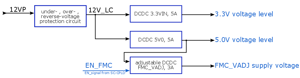
Figure 3: Power-Up On sequence diagram.
Configuring VCCIO
On the TE0705 carrier board different VCCIO configurations can be chosen are selectable by jumper J21 and DIP-switch S3.
The purpose of the jumper and the DIP-switch S3 of the Carrier Board will be explained in the following sections.
...
VCCIO
...
Voltage Level DIP-Switch S3
There is the possibility to select the module's PL IO-bank's supply voltage VIOTB to fixed adjustable voltages VADJ. Therefore, the jumper J21 has to be set to the position 1, 2-3, to connect the pins 'VIOTB' and 'ADJ'. On position 1-2, 3, the supply voltage VIOTB will be fixed to 3.3V
Table 3 shows the switch-configuration of the DIP-switch S3 to set the voltage VADJ.
Note: The configuration of VADJ depends on the used firmware of the System-Controller-CPLD. For detailed information, refer to the documentation of the TE0705 System-Controller-CPLD.
With jumper J21, user can select between two different power sources for SoM PL IO banks supply voltage VIOTB. If set to position 1-2, fixed 3.3V is selected as VIOTB source. If set to position 2-3, FMC_VADJ is selected as VIOTB source. Voltage level of FMC_VADJ depends on the settings of DIP-switch S3, see table below:
| J21 Position |
|---|
S3-1 (CM1) | S3-2 ( |
|---|
CM0) | FMC_VADJ |
|---|
Voltage | VIOTB Voltage | Notes | |||
|---|---|---|---|---|---|
| 1-2 | - | - | - | 3.3V | |
| 2-3 | OFF | OFF | 1.8V | 1.8V | |
| 2-3 | ON | OFF |
2.5V | 2.5V | |
| 2-3 | OFF | ON |
3.3V | 3.3V | ||
| 2-3 | ON | ON | 1.8V |
Table 3: Switch S3 positions for fixed values of the VADJ voltage
| 1.8V | This setting also enables JTAG access to the System Controller CPLD on the SoM via B2B connector JB2. |
Table 3: Jumper J21 and DIP-switch S3 settings for VIOTB voltage configuration.
Note: Exact function of the S3-1 and S3-2 switches depend on the TE0705 System Controller CPLD firmware. For more detailed information, refer to the documentation of the TE0705 System Controller CPLD.
Configuring Power Supply of the Micro USB Connector (Device, Host or Configuring Power Supply of the Micro USB Connector (Device, Host or OTG Modes)
The TE0705 carrier board can be configured as a USB host device. Hence, it must provide from 5.25V to 4.75V to the board side of the downstream connection (micro USB port on J12). To provide sufficient power, a TPS2051 power distribution switch is located on the carrier board in between the 5V power supply and the Vbus signal of the USB downstream port interface. If the output load exceeds the current-limit threshold, the TPS2051 limits the output current and pulls the overcurrent over-current logic output (OC_n) low, which is routed to the on-board CPLD. The TPS2051 is put into operation by setting J19 CLOSED. J20 provides an extra 100µF decoupling capacitor (in addition to 10µF) to further stabilize the output signal. Moreover, a series terminating resistor of either 1K (J9: 1-2, 3) or 10K (J9: 1, 2-3) is selectable on the "USB-VBUS" signal. Both signals, USB-VBUS and VBUS_V_EN (that enables the TPS2051 on "high") are routed (as well as the corresponding D+/- data lines) via the on-board connector directly to the USB 2.0 high-speed transceiver PHY on the mounted SoM, which is, in turn, connected to the Zynq FPGA. In summary, the default jumper settings are the following: J9: 1-2, 3 (1K series terminating resistor); J19: CLOSED (TPS2051 in operation); J20: CLOSED (100 µF added).
Additionally, the TE0705 carrier board is equipped with a second mini USB port J7 that is connected to a "USB to multi-purpose UART/FIFO IC" from FTDI (FT2232HQFT2232H) and provides a USB-to-JTAG interface between a host PC and the TE0705 carrier board and the Zynq-modulemounted SoM, respectively. Because it acts as a USB function device, no power switch is required (and only a ESD protection must be provided) in this case.
Summary of VCCIO
...
Configuration
All B2B VCCIO supply voltages to the 4 x 5 On the TE0705 carrier board all PL IO-bank's supply voltages of the 4x5 SoM (VCCIOA, VCCIOB, VCCIOC and VCCIOD, VCCIOD; see 4x5 4 x 5 Module Integration Guide) are connected to the VCCIO-voltage 3.3V VIOTB, which is either fixed to 3.3V (J21: 1-2, 3) or selectable with the adjustable supply-voltage FMC_VADJ (J21: 1, 2-3). The supply-voltages have following pin assignments on B2B-connectors:
base-board
baseboard supply-voltages |
|---|
...
| baseboard B2B connector-pins | standard assignment of PL IO-bank supply-voltages on TE 4x5 module's B2B connectors |
|---|
...
| baseboard voltages and signals connected with | |||
|---|---|---|---|
| VIOTB | JB1-10, JB1-12, JB2-2, JB2-4, JB2-6, JB2-8, JB2-10 | VCCIOA (JM1-9, JM1-11), VCCIOB (JM2-1, JM2-3), VCCIOC (JM2-5), VCCIOD (JM2-7, JM2-9) | VCCIO3 ( |
...
System Controller |
...
CPLD pin 5, 11, 23), J15 VTREF, J11, J13, J2, J5 and J6 VCCIO |
Table 4:
...
baseboard supply-voltage VIOTB
...
.
| Note |
|---|
Note: The corresponding PL IO-voltage supply voltages of the |
...
4 x 5 SoM to the selectable |
...
baseboard voltage VIOTB are depending on the mounted |
...
4 x 5 SoM and varying in order of the used model. Refer to SoM's schematic to get information about the specific pin assignment on module's B2B-connectors regarding PL IO-bank supply voltages and to the |
...
4 x 5 Module integration Guide for VCCIO voltage options. |
...
Following table describes how to configure the
...
baseboard supply-voltages by jumpers:
...
baseboard supply-voltages vs voltage-levels | VIOTB | USB-VBUS |
|---|---|---|
| 3V3 | J21:1-2, 3 | - |
| VADJ | J21:1, 2-3 | - |
| 5V0 intern | - | J9:1-2, 3 & J19: 1-2 (J20: 1-2: additional decoupling-capacitor 100 µF) |
| Vbus extern | - | J9: 1, 2-3 & J19: open |
Table 5: Configuration of
...
baseboard supply-voltages via jumpers. Jumper-Notification: 'Jx: 1-2, 3' means pins 1 and 2 are connected, 3 is open. 'Jx: 1, 2-3' means pins 2 and 3 are connected, 1 is open.
| Note |
|---|
...
Power On Reset (POR)
On the TE0705 the 5.0V and 3.3V power supply rails are generated by high performance DC-DC-converters from the external 12V supply. While the 3.3V plane supplies several on-board components (e.g., Lattice CPLD and FTDI Dual USB UART/FIFO IC), the 5V plane is mainly provided to power supply of the module to be carried (e.g., TE0720 Zynq SoC module). For the latter, however, special considerations must be taken (see TE0720 Power Supply). Therefore, the on-module system controller (SC) must be provided with information about the power-on-reset (POR) process, namely, the following control signals EN1, RESIN, and NOSEQ. And the SC provides, in turn, the status signal PGOOD down to the on-board System-Controller-CPLD.
...
This signal is controlled by the user push button S1 on the TE0701 and is forwarded directly to the SC, where it is latched together with the EN1 signal as well as the “all power rails OK” signal (1.0V and 1.8V for core; 1.5V and VTT for RAM, and 3.3V).
| Info |
|---|
The 3.3V power supply rail can be switched on (EN_3V3=’1’) or off (EN_3V3=’0’) by a load switch (TPS27082L) and is continuously checked by a voltage detector (TPS3805H33). Note: The 3.3VIN power supply (from which the 3.3V power plane is sourced) is supplied by the TE0701 Carrier Board and is kept always on! |
When RESIN (alias user push button S1) is not pushed and simultaneously the EN1 signal is asserted (EN='1') and all power rails are ok, the active-high Zynq power-on-reset signal PS_POR_B is asserted.
...
Table 6: Generation of PGOOD-signal
| Info |
|---|
| For more information on the preceding signals please consult the corresponding Wiki documentation of the TE0720 System Management Controller. |
Technical Specifications
Absolute Maximum Ratings
...
Vin supply voltage
...
11.4
...
V
...
Storage Temperature
...
°C
...
Recommended Operating Conditions
...
Physical Dimensions
Board size: PCB 170.4 mm × 98 mm. Notice that some parts the are hanging slightly over the edge of the PCB like the mini USB-jacks (ca. 1.4 mm) and the Ethernet RJ-45 jack (ca 2.2 mm), which determine the total physical dimensions of the carrier board. Please download the assembly diagram for exact numbers.
Mating height of the module with standard connectors: 8mm
PCB thickness: ca. 1.65mm
Highest part on the PCB is the Ethernet RJ-45 jack, which has an approximately 17 mm overall hight. Please download the step model for exact numbers.
All dimensions are given in mm.
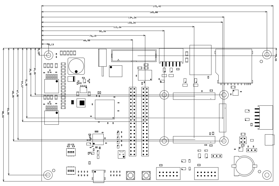
Figure 4: Physical Dimensions of the TE0705-04 carrier board
Operating Temperature Ranges
Commercial grade: 0°C to +70°C.
Board operating temperature range depends also on customer design and cooling solution. Please contact us for options.
Weight
ca. 110 g - Plain board
Document Change History
...
0.1
...
Ali Naseri
...
Initial document
Hardware Revision History
...
Notes
...
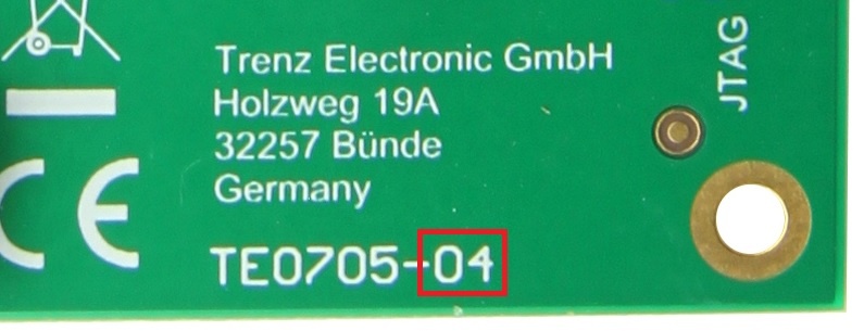
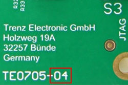
Figure 5: Hardware revision Number
...
Take care of the VCCO voltage ranges of the particular PL IO-banks (HR, HP) of the mounted SoM, otherwise damages may occur to the FPGA. Therefore, refer to the TRM of the mounted SoM to get the specific information of the voltage ranges. It is recommended to set and measure the PL IO-bank supply-voltages before mounting of TE 4 x 5 module to avoid failures and damages to the functionality of the mounted SoM. |
Board to Board Connectors
| Include Page | ||||
|---|---|---|---|---|
|
Technical Specifications
Absolute Maximum Ratings
| Parameter | Min | Max | Units | Notes |
|---|---|---|---|---|
VIN supply voltage | 11.4 | 12.6 | V | 12.0V supply voltage ± 5% |
Storage temperature | -55 | 125 | °C | Lattice MachX02 family data sheet |
Recommended Operating Conditions
| Parameter | Min | Max | Units | Notes |
|---|---|---|---|---|
| VIN supply voltage | 11.4 | 12.6 | V | - |
Physical Dimensions
Board size: 170.4 mm × 98 mm. Note that few parts are slightly hanging over the PCB edge, like mini USB jacks (ca. 1.4 mm) and the Ethernet RJ-45 jack (ca 2.2 mm), which determine the total physical dimensions of the carrier board. Please download the assembly diagram for exact numbers.
Mating height of the module with standard connectors: 8 mm.
PCB thickness: ca. 1.65 mm.
Highest part on the PCB is the Ethernet RJ-45 jack (approximately 17 mm). Please download the step model for exact numbers.
All dimensions are given in millimeters.
Figure 4: Physical dimensions of the TE0705-04 carrier board.
Operating Temperature Ranges
Commercial grade: 0°C to +70°C.
Board operating temperature range depends also on customer design and cooling solution. Please contact us for options.
Weight
Approximately 110 g - Plain board.
Revision History
Hardware Revision History
| Date | Revision | Notes | PCN | Documentation link |
|---|---|---|---|---|
| 2016-10-04 | 04 | - | - | TE0705-04 |
Figure 5: Hardware revision number.
Hardware revision number is printed on the PCB board next to the model number separated by the dash.
Document Change History
| Date | Revision | Contributors | Description | ||||||||||||||||||||||||||
|---|---|---|---|---|---|---|---|---|---|---|---|---|---|---|---|---|---|---|---|---|---|---|---|---|---|---|---|---|---|
|
|
|
| ||||||||||||||||||||||||||
| 2020-08-19 | v.18 | John Hartfiel |
| ||||||||||||||||||||||||||
| 2019-06-27 | v.17 | John Hartfiel |
| ||||||||||||||||||||||||||
| 2019-03-14 | v.16 | John Hartfiel |
| ||||||||||||||||||||||||||
| 2017-02-08 | V.11 | Ali Naseri, Jan Kumann |
| ||||||||||||||||||||||||||
| -- | all |
|
|
Disclaimer
| Include Page | ||||
|---|---|---|---|---|
|
Overview
Content Tools