Page History
...
Block Diagram
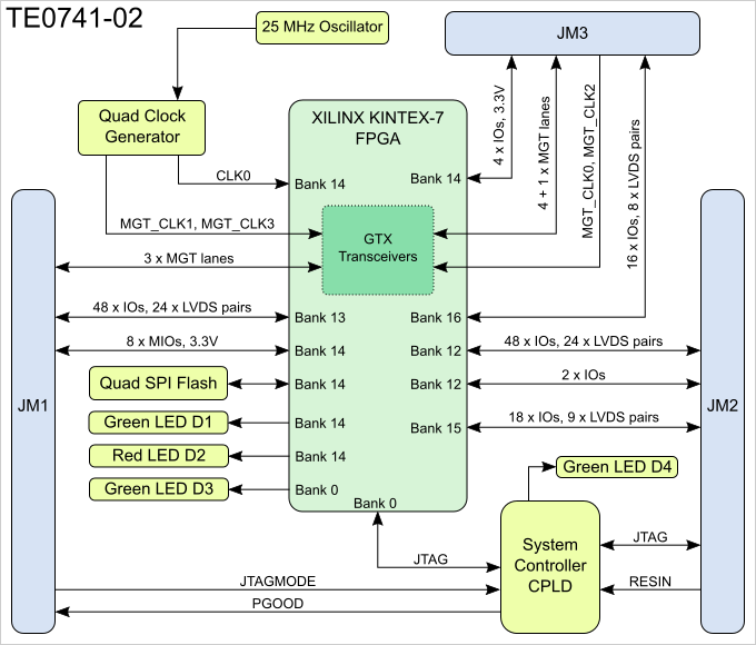
Figure 1: TE0741 Block Diagramdiagram.
Main Components
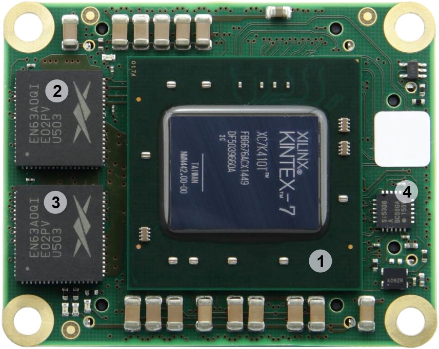
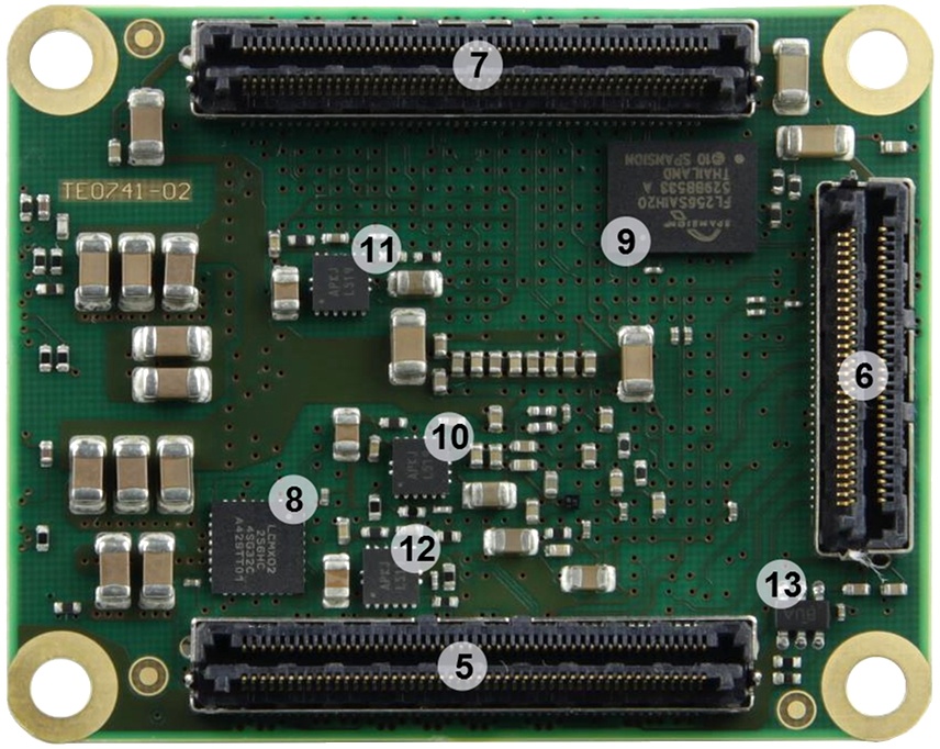
Figure 2: TE0741 (REV -02 )module.
- Xilinx Kintex-7 FPGA (Kintex-7), U1
- EN63A0QI Voltage Regulator 1.0V (Slave), U15
- EN63A0QI Voltage Regulator 1.0V (Master), U14
- Programmable PLL clock generator, U2
- B2B connector JM1 (Samtec Razor Beam™ LSHM-150 ) B2B connector JM3 (, JM1
- Samtec Razor Beam™ LSHM-130 ) B2B connector, JM3
- JM2 (Samtec Razor Beam™ LSHM-150 )B2B connector, JM2
- System Controller CPLD (Lattice LCMXO2-256HC), U7
- 32 - MByte Quad SPI Flash memory, U4
- EP53F8QI Voltage Regulator 1.8V, U8
- EP53F8QI Voltage Regulator 1.0V MGTAVCC, U16
- EP53F8QI Voltage Regulator 1.2V MGTAVTT, U6
- TPS27082L load switch for 3.3V voltage level, Q1
Key Features
- Industrial-grade Xilinx Kintex-7 FPGA module (70T*, 160T*, 325T, 410T)
* Devices supported by the free Xilinx Vivado WebPACK software. - 256-Mbit (32-MByte) Quad SPI Flash memory (for configuration and operation) accessible through:
- FPGA
- JTAG port (SPI indirect (Bus width x4))
- 8 GTX transceivers
- FPGA configuration through:
- JTAG (B2B connector)
- SPI Flash memory
- 25 MHz low jitter oscillator with shutdown control
- Programmable quad PLL clock generator
- On-board high-efficiency DC-DC converters
- GTX voltage regulators with control enable
- Core voltage regulator: 20A (2 x Enpirion DC-DC regulators with load-sharing)
- Supply voltages: either 3.3V or 3.3V and 5V
- Plug-on module with two 100-pin and one 60-pin high-speed hermaphroditic stacking strips
- Up to 144 (94 for 70T) FPGA I/O pins available on B2B strips (up to 65 LVDS pairs possible)
- 2 user LED's, 1 DONE FPGA pin LED, 1 System Controller status LED
- System management and power sequencing
- AES bit-stream encryption
- eFUSE bit-stream encryption
- Evenly spread supply pins for good signal integrity
- Assembly options for cost or performance optimization available on request
...
Hardware revision number is written on the PCB board together with the module model number separated by the dash.

Document Change History
| Date | Revision | Contributors | Description |
|---|---|---|---|
| 2017-01-22 | Jan Kumann | New block diagram added. | |
| 2017-01-13 | V38 | Jan Kumann | New product images and physical dimension drawings. Formatting improvements and small corrections. |
| 2017-01-12 | V21 | John Hartfiel | Correction: B2B and FPGA Bank location. |
| 2016-12-14 | V19 | Ali Naseri | TRM revision. |
| 2013-12-02 |
| V1 | Antti Lukats, Jon Bean | Initial version. |
Disclaimer
| Include Page | ||||
|---|---|---|---|---|
|
...
Overview
Content Tools