Page History
...
| Scroll Title | ||||||||||||||||||||||||||||||||||
|---|---|---|---|---|---|---|---|---|---|---|---|---|---|---|---|---|---|---|---|---|---|---|---|---|---|---|---|---|---|---|---|---|---|---|
| ||||||||||||||||||||||||||||||||||
|
Main Component
| Scroll Title | ||||||||||||||||||||||||||||||||||
|---|---|---|---|---|---|---|---|---|---|---|---|---|---|---|---|---|---|---|---|---|---|---|---|---|---|---|---|---|---|---|---|---|---|---|
| ||||||||||||||||||||||||||||||||||
|
...
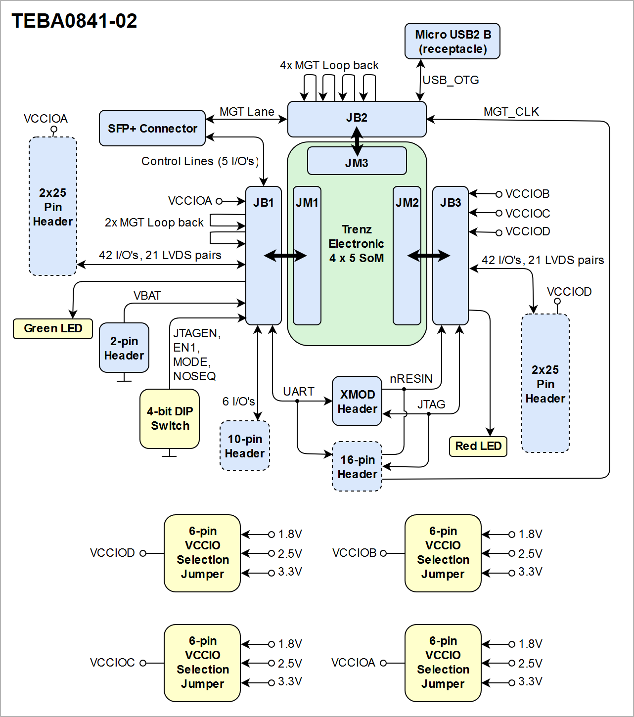
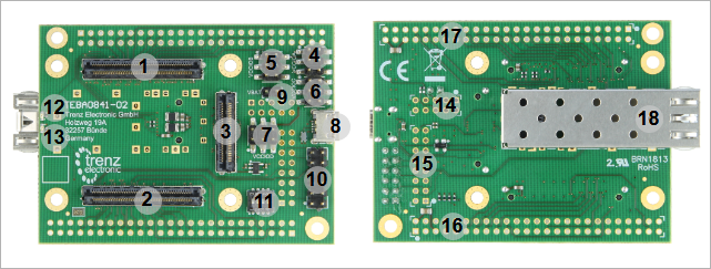
- Samtec Razor Beam™ LSHM-150 B2B connector, JB1
- Samtec Razor Beam™ LSHM-150 B2B connector, JB3
- Samtec Razor Beam™ LSHM-130 B2B connector, JB2
- 6-pin header J26, for selecting PL I/O-bank voltage
- 6-pin header J27J5, for selecting PL I/O-bank voltage
- Micro USB2 Type B connector J12 (Device or OTG mode)
- XMOD FTDI JTAG/UART header, JX1
- 6-pin header J6, for selecting PL I/O-bank voltage
- 6-pin header J27, for selecting PL I/O-bank voltage
- Micro USB2 Type B connector J10 (Device or OTG mode)
- 2-pin VBAT header J7
- XMOD FTDI JTAG/UART header, JX1
- 4-bit DIP-switch S1
- User User LED D1 (green)
- User LED D2 (red)
- SFP+ Connector, J1
- 5010-pin header soldering-pads J17, for access to PL J4, 6 I/O-bank pins (42 I/O'S, 21 LVDS pairs's available
- 16-pin header soldering-pads J3, JTAG/UART header ('XMOD FTDI JTAG Adapter'-compatible pin-assignment)
- 50-pin header soldering-pads J20J17, for access to PL I/O-bank pins (42 I/O'S, 21 LVDS pairs)
- 1650-pin header soldering-pads J3, JTAG/UART header ('XMOD FTDI JTAG Adapter'-compatible pin-assignment)10-pin header soldering-pads J4, 6 I/O's availableJ20, for access to PL I/O-bank pins (42 I/O'S, 21 LVDS pairs)
- SFP+ Connector, J1
Initial Delivery State
Board is shipped in following configuration:
...
There are one 4-bit DIP-witches S1 present on the TEBA0841 board to configure options and set parameters. The following table describes the of the particular switches:
| DIP-switch S1 | usage | Default | Signal Schematic Name | Connected to | Notes | Note | ||
|---|---|---|---|---|---|---|---|---|
| S1-1 | OFF module FPGA access | OFF(GND)S1A | BOOTMODE | JB1-90 | The functionalities of all DIP-switches is dependent on the mounted The DIP-switch sets control signals, which are usually routed to the So refer to the Wiki reference page of the SC CPLD firmware of the SoM. | |||
| S1B | EN1 | JB1-27 | ||||||
| S1C | MODE | JB1-31 | ||||||
| only used for module with CPLD | ||||||||
| S1-2 | OFF enabled ON disabled | OFF(VDD) | EN1 | JB1-27 | power enable, some modules can't disable power in this case it has normally the same effect like the reset pin | |||
| S1-3 | OFF QSPI Boot ON SD Boot | OFF(VDD) | MODE | JB1-31 | Boot mode selection, only for Zynq and ZynqMP devices, on FPGA modules not matter (always QSPI). JTAG is on all modes available | |||
| S1-4 | OFF enabled ON disabled | OFF(VDD) | NOSEQ | JB1-8 | power sequencing, only on some modules supported. Otherwise it's unused or can be reused by customer | S1D | NOSEQ | JB1-8
Table 12: DIP-switch S1, see also 4x5 Module Controller IOs
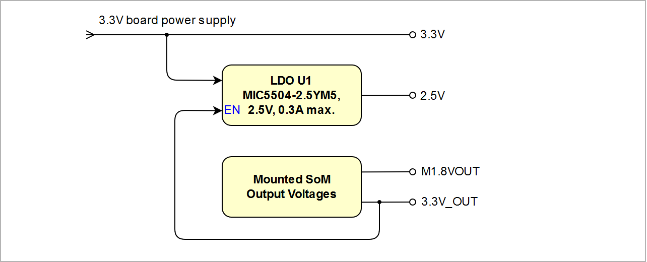
VCCIO Selection Jumper
On the TEBA0841 carrier board different VCCIO configurations can be selected by the jumper header J26, J27, J5 and J6.
...
The external power-supply can be connected to the board by the following pins:
| Connector | 3.3V pin | GND pin | JX1||
|---|---|---|---|---|
JX1-5, JX1-6, | JX1-1, JX1-2 | J3 | J3-5, J3-6 | J3-1, J3-2 |
| J4 | J4-5 | J4-1, J4-2 | ||
| J20 | J20-5, J20-46 | J20-1 , J20-2 , J20-49 , J20-50 | ||
| J17 | J17-5, J17-46 | J17-1 , J17-2 , J17-49 , J17-50 |
...
| Scroll Title | ||||||||||||||||||||||||||||||||||
|---|---|---|---|---|---|---|---|---|---|---|---|---|---|---|---|---|---|---|---|---|---|---|---|---|---|---|---|---|---|---|---|---|---|---|
| ||||||||||||||||||||||||||||||||||
|
Power Rails
The voltage direction of the power rails is from board and on-board connectors' view:
...
| Jumper / Header Designator | VCC / VCCIO | Direction | Pins | Notes |
|---|---|---|---|---|
| J26 | VCCIOA | In | 2, 4, 6 | - |
| M1.8VOUT | Out | 1 | - | |
| 2.5V | Out | 3 | - | |
| 3.3V_OUT | Out | 5 | - | |
| J27 | VCCIOD | In | 2, 4, 6 | - |
| M1.8VOUT | Out | 1 | - | |
| 2.5V | Out | 3 | - | |
| 3.3V_OUT | Out | 5 | - | |
| J5 | VCCIOB | In | 2, 4, 6 | - |
| M1.8VOUT | Out | 1 | - | |
| 2.5V | Out | 3 | - | |
| 3.3V_OUT | Out | 5 | - | |
| J6 | VCCIOC | In | 2, 4, 6 | - |
| M1.8VOUT | Out | 1 | - | |
| 2.5V | Out | 3 | - | |
| 3.3V_OUT | Out | 5 | - | |
| J7 | VBAT | In | 1 | - |
...
| Scroll Title | ||||
|---|---|---|---|---|
| ||||
|
Document Change History
...
Date | Revision | Contributors | Description | ||||||||||||||||||||||||||
|---|---|---|---|---|---|---|---|---|---|---|---|---|---|---|---|---|---|---|---|---|---|---|---|---|---|---|---|---|---|
|
|
|
| ||||||||||||||||||||||||||
| 2019-09-17 | v.82 | John Hartfiel |
| ||||||||||||||||||||||||||
| 2018-07-13 | v.81 | John Hartfiel |
| ||||||||||||||||||||||||||
| 2018-07-10 | v.78 | John Hartfiel |
| ||||||||||||||||||||||||||
| v.75 | Ali Naseri, Jan Kumann |
|
...
Overview
Content Tools