Page History
| Scroll Ignore |
|---|
Download PDF Version of this Document. |
| Scroll pdf ignore | ||||
|---|---|---|---|---|
Table of Contents
|
Overview
| Scroll Only (inline) |
|---|
OnlineRefer to https://shop.trenz-electronic.de/en/Download/?path=Trenz_Electronic/carrier_boards/TE0705 for downloadable version of this manual and otheradditional relatedtechnical documentsdocumentation canof be found at https://wiki.trenz-electronic.de/display/PD/TE0701 the product. |
...
- ARM JTAG Connector (DS-5 D-Stream) J15 - PJTAG to EMIO multiplexing needed
- 12-pin IDC header socket J1 (right angle, max. VCCIO-voltage: 3.3V): mapped to 8 Zynq PS MIO0-bank-pins (MIO0, MIO9 to MIO15), 6 pins (MIO10 to MIO15) are additionally connected to TE0705 System-Controller-CPLD
RJ45 GbE Connector
- SD Card Socket - Zynq SDIO0 Bootable SD port
- 12-pin IDC header socket (right angle) J2 for access to Zynq-module's PL IO-bank pins (not usable as LVDS-pairs, only single-ended IOs, max. VCCIO-voltage: VIOTB)
- Micro USB Connector J12 (Device, Host or OTG Modes)
- Battery holder for CR1220 (RTC backup voltage)
- 12-pin IDC header socket (vertical) J5 for access to Zynq-module's PL IO-bank pins (4 LVDS-pairs, max. VCCIO-voltage: VIOTB)
- 12-pin IDC header socket (vertical) J6 for access to Zynq-module's PL IO-bank pins (4 LVDS-pairs, max. VCCIO-voltage: VIOTB)
- User Push-Button S2 ("RESTART" button by default)
- User Push-Button S1 ("RESET" button by default)
- User LEDs D6, D7, D8, D9 (function mapping depends on firmware of System-Controller-CPLD)
- User LEDs D4, D5, D14, D15 (same as above)
- Mini USB Connector (USB JTAG and UART Interface) J7
- User 4-bit DIP-Switch S3
- User 4-bit DIP-Switch S4
- FTDI FT2232HQ USB 2.0 High Speed to UART/FIFO
- Lattice Semiconductor MachXO2 1200HC System-Controller-CPLD
- Jumper J4 to fix user button S2 to switched state
- 40-Pin-Header J13 for access to PL IO-bank-pins
- 40-Pin-Header J11 for access to PL IO-bank-pins
- Samtec Razor Beam™ high-speed hermaphroditic 50 positions terminal strip, board to board connector, LSHM-150 B2B connector JB1
- Samtec Razor Beam™ high-speed hermaphroditic 50 positions terminal strip, board to board connector, LSHM-150 B2B connector JB2
- Samtec Razor Beam™ high-speed hermaphroditic 50 positions terminal strip, board to board connector, LSHM-130 B2B connector JB3
- Barrel jack for 12V Power Supply J10
- Jumper J21 to select supply voltage VIOTB
- Jumper J9, J19, J20 to select supply voltage USB-VBUS
...
Note: The configuration of VADJ depends on the used firmware of the System-Controller-CPLD. For detailed information, refer to the documentation of the TE0705 System-Controller-CPLD.
S3-1 (CM1) | S3-2 (CM2) | VADJ Value |
|---|---|---|
OFF | OFF | 1.8V |
OFF | ON | 2.5V |
ON | OFF | 3.3V |
ON | ON | 1.8V (Note: Also Zynq-module's SC-CPLD JTAG-access is enabled, see section JTAG in the documentation of the TE0705 System-Controller-CPLD.) |
Table 3: Switch S3 positions for fixed values of the VADJ voltage
...
On the TE0705 carrier board all PL IO-bank's supply voltages of the 4x5 SoM (VCCIOA, VCCIOB, VCCIOC, VCCIOD; see 4x5 Module Integration Guide) are connected to the VCCIO-voltage VIOTB, which is either fixed to 3.3V (J21: 1-2, 3) or selectable with the adjustable supply-voltage VADJ (J21: 1, 2-3). The supply-voltages have following pin assignments on B2B-connectors:
base-board supply-voltages | base-board B2B connector-pins | standard assignment of PL IO-bank supply-voltages on TE 4x5 module's B2B connectors | base-board voltages and signals connected with |
|---|---|---|---|
| VIOTB | JB1-10, JB1-12, JB2-2, JB2-4, JB2-6, JB2-8, JB2-10 | VCCIOA (JM1-9, JM1-11), VCCIOB (JM2-1, JM2-3), VCCIOC (JM2-5), VCCIOD (JM2-7, JM2-9) | VCCIO3 (Systm-Controller-CPLD pin 5, 11, 23), J15 VTREF, J11, J13, J2, J5 and J6 VCCIO |
Table 4: base-board supply-voltage VIOTB
| Note |
|---|
Note: The corresponding PL IO-voltage supply voltages of the 4x5 SoM to the selectable base-board voltage VIOTB are depending on the mounted 4x5 SoM and varying in order of the used model. Refer to SoM's schematic to get information about the specific pin assignment on module's B2B-connectors regarding PL IO-bank supply voltages and to the 4x5 Module integration Guide for VCCIO voltage options. |
Following table describes how to configure the base-board supply-voltages by jumpers:
base
Base-board supply-voltages vs voltage-levels | VIOTB | USB-VBUS |
|---|---|---|
| 3V3 | J21:1-2, 3 | - |
| VADJ | J21:1, 2-3 | - |
| 5V0 intern | - | J9:1-2, 3 & J19: 1-2 (J20: 1-2: additional decoupling-capacitor 100 µF) |
| Vbus extern | - | J9: 1, 2-3 & J19: open |
Table 5: Configuration of base-board supply-voltages via jumpers. Jumper-Notification: 'Jx: 1-2, 3' means pins 1 and 2 are connected, 3 is open. 'Jx: 1, 2-3' means pins 2 and 3 are connected, 1 is open
| Note |
|---|
| It is recommended to set and measure the PL IO-bank supply-voltages before mounting of TE 4x5 module to avoid failures and damages to the functionality of the mounted SoM. |
Power On Reset (POR)
On the TE0705 the 5.0V and 3.3V power supply rails are generated by high performance DC-DC-converters from the external 12V supply. While the 3.3V plane supplies several on-board components (e.g., Lattice CPLD and FTDI Dual USB UART/FIFO IC), the 5V plane is mainly provided to power supply of the module to be carried (e.g., TE0720 Zynq SoC module). For the latter, however, special considerations must be taken (see TE0720 Power Supply). Therefore, the on-module system controller (SC) must be provided with information about the power-on-reset (POR) process, namely, the following control signals EN1, RESIN, and NOSEQ. And the SC provides, in turn, the status signal PGOOD down to the on-board System-Controller-CPLD.
...
Technical Specifications
Absolute Maximum Ratings
| Parameter | Min | Max | Units | Notes |
|---|
VIN supply voltage | 11.4 | 12.6 | V | 12.0V supply voltage ± 5% |
Storage |
temperature | -55 | 125 | °C | Lattice MachX02 family data sheet |
Recommended Operating Conditions
...
Physical Dimensions
Board size: PCB 170.4 mm × × 98 mm. Notice Note that some few parts the are are slightly hanging slightly over the PCB edge of the PCB , like the mini USB - jacks (ca. 1.4 mm) and the Ethernet RJ-45 jack (ca 2.2 mm), which determine the total physical dimensions of the carrier board. Please download the assembly diagram for exact numbers.
Mating height of the module with standard connectors: 8mm8 mm.
PCB thickness: ca. 1.65mm65 mm.
Highest part on the PCB is the Ethernet RJ-45 jack , which has an (approximately 17 mm overall hight). Please download the step model for exact numbers.
All dimensions are given in mmmillimeters.
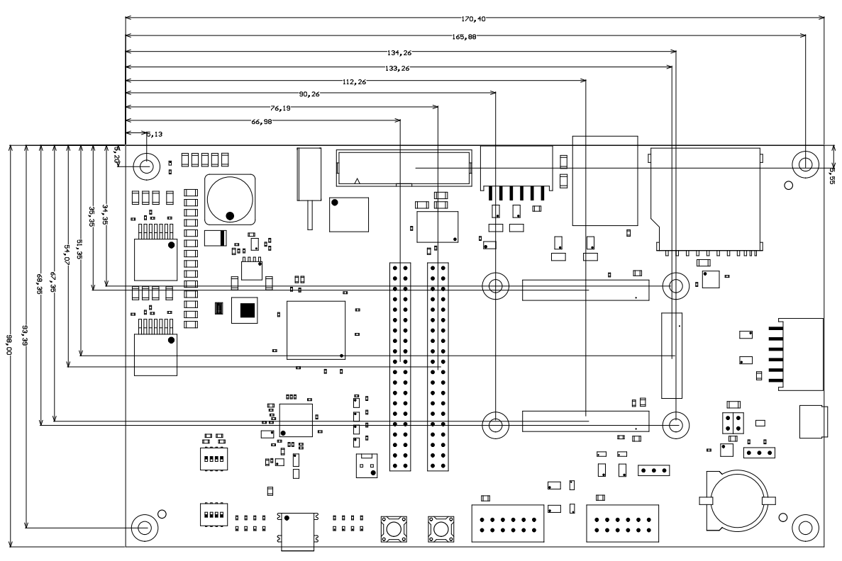
Figure 4: Physical Dimensions dimensions of the TE0705-04 carrier board.
Operating Temperature Ranges
...
Board operating temperature range depends also on customer design and cooling solution. Please contact us for options.
Weight
ca. Approximately 110 g - Plain board.
Document Change History
...
0.1
...
Ali Naseri
...
Initial document
Revision History
Hardware Revision History
| Date | Revision | Notes | PCN | Documentation link |
|---|---|---|---|---|
| 2016-10-04 | 04 | |||
| - | 03 | |||
| - | 02 | |||
| - | 01 |
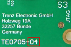
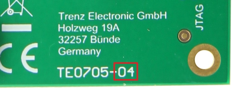
Figure 5: Hardware revision Numbernumber.
Hardware revision number is printed on the PCB board next to the model number separated by the dash.
Document Change History
| Date | Revision | Contributors | Description |
|---|---|---|---|
| 2017-01-18 | Ali Naseri, Jan Kumann | TRM for TE0705-04 | |
| 2017-01-15 | 0.1 | Ali Naseri | Initial document. |
Hardware Revision History
| Date | Revision | Notes | PCN | Documentation Link |
|---|---|---|---|---|
| 2016-10-04 | 04 | |||
| - | 03 | |||
| - | 02 | |||
| - | 01 |
Disclaimer
| Include Page | ||||
|---|---|---|---|---|
|
Overview
Content Tools