Page History
| Scroll Ignore |
|---|
Download PDF Version version of this Documentdocument. |
| Scroll pdf ignore | |
|---|---|
Table of Contents
|
...
The Trenz Electronic TE0705 carrier board provides functionality for testing, evaluation and development purposes of company's 4 x 5 cm SoMs (System on Module). Carrier The carrier board is equipped with a broad range of various components and connectors for different configuration setups and needs. On-module functional components and multipurpose I/Os of the SoM's PL and PS logic are connected via board-to-board connectors to the carrier board components and connectors for easy user access.
See "4 x 5 cm carriers" page for more information about supported 4 x 5 cm SoMs.
Block Diagram
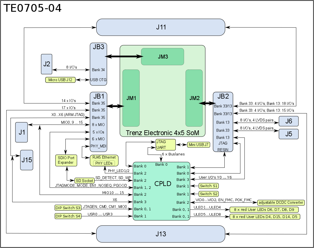
Figure 1: TE0705-04 Block Diagram.
...
- ARM JTAG Connector (DS-5 D-Stream) J15 - PJTAG to EMIO multiplexing needed
- 12-pin IDC header socket J1 (right angle, max. VCCIO voltage 3.3V)
RJ45 GbE Connector
- SD Card Socket - Zynq SDIO0 Bootable SD port
- 12-pin IDC header socket (right angle) J2
- Micro USB Connector J12 (Device, Host or OTG Modes)
- Battery holder for CR1220 (RTC backup voltage)
- 12-pin IDC header socket (vertical) J5
- 12-pin IDC header socket (vertical) J6
- User Push-Button S2 ("RESTART" button by default)
- User Push-Button S1 ("RESET" button by default)
- User LEDs D6, D7, D8, D9
- User LEDs D4, D5, D14, D15
- Mini USB Connector (USB JTAG and UART Interface) J7
- User 4-bit DIP-Switch S3
- User 4-bit DIP-Switch S4
- FTDI FT2232HQ USB 2.0 High Speed to UART/FIFO
- Lattice Semiconductor MachXO2 1200HC System Controller CPLD
- Jumper J4 to fix user button S2 to switched state
- 40-Pin-Header J13 for access to PL IO-bank-pins
- 40-Pin-Header J11 for access to PL IO-bank-pins
- Samtec Razor Beam™ LSHM-150 B2B connector JB1
- Samtec Razor Beam™ LSHM-150 B2B connector JB2
- Samtec Razor Beam™ LSHM-130 B2B connector JB3
- Barrel jack for 12V power supply J10
- Jumper J21 to select supply voltage of VIOTB
- Jumper J9, J19, J20 to select supply voltage of USB-VBUS
Key Features
- Overvoltage-, undervoltage - and reversed- reverse supply -voltage- protection controller
- Barrel jack for 12V power supply
- Carrier Board On-board System Controller CPLD (Lattice MachXO2 1200HC), programable by programmable via Mini-USB JTAG -Interface interface J7
- SoM programable by ARM-JTAG-Interface-Connector can be programmed via ARM JTAG interface connector (J15) or by through System Controller CPLD via Mini-USB JTAG -Interface interface J7
- RJ45 Gigabit Ethernet MagJack with 2 integrated LEDs
- 2x 2 x 40-Pin-Header pin headers J11 and J13 for access to module's PL IO - bank - pins
- USB JTAG- and /UART -Interface interface (FTDI FT2232HQ) with Mini-USB -Connector connector J7
- 8 x user LEDs (red) routed to System Controller CPLD, 8 x red
- 2 x user-push button buttons routed to System Controller CPLD; by . By default (depending on CPLD -Firmwarefirmware) configured as system "RESET" and "RESTART" buttonbuttons
- 2 x 4-bit DIP-Switch switch for baseboard - configuration
- 2 x 12-pin IDC header socket (vertical) J5, J6 for access to accessing module's PL IO - bank - pins, usable can be used as LVDS pairs
- 2 x 12-pin IDC header socket (right angle) J1 and J2 for access to accessing module's PL IO - bank - pins or PS MIO0 - bank - pins (if used with Zynq - module mounted)
- 2 x 50-pin IDC header J11, J13 for accessing module's PL IO bank pins
- Micro SD card socket with card detect switch, can be used for system bootingMicro SD card socket, can be used to boot system
- Micro-USB -Interface interface (J12) connected to SoM's USB transceiver (Device, Host or OTG modes)
- Trenz Electronic 4 x 5 cm module Socket connectors (3 x Samtec LSHM series connectors)
Interfaces and Pins
Micro SD Card Socket
Micro SD Card card socket is not directly wired connected to the B2B connector pins, but through a Texas Instruments TXS02612 SDIO Port Expander , which is needed for voltage translation due to different voltage levels of the Micro SD Card and MIO-bank of the Xilinx Zynq-module. The Micro SD Card card has 3.3V signal voltage level , but the MIO-bank on the Xilinx Zynq-module has VCCIO while Xilinx Zynq MIO bank uses 1.8V for VCCIO.
Dual channel USB to UART/FIFO
The TE0705 Carrier Board TE0701 carrier board has on-board USB 2.0 High Speed to UART/FIFO IC FT2232HQ from FTDI. Channel A can be used as JTAG interface Interface (MPSSE) to program the System Controller CPLD, Channel B can be used as UART interface Interface routed to CPLD. There are also 6 additionally additional bus-lanes available for user-specific use. The FT2232HQ-Chip can also be used as FIFO in FT245 asynchronous mode.
There is also a standard 256 Byte EEPROM connected to the FT2232HQ-chip available to store custom configuration settings. EEPROM settings can be changed
| Note |
|---|
| Warning: When using FTDI |
...
| software tools, the 256 byte user EEPROM can be erased without confirmation. As a consequence, the Digilent license stored in that EEPROM will also be deleted. |
USB Interface
The TE0705 carrier board has two physical USB - connectors:
- J7 as mini-USB - connector wired to on-board FTDI FT2232HQ chip.
- J12 as micro-USB - connector wired to B2B connector JB3 (usually there is usually an USB - transceiver on the SoMsSoM).
JTAG Interface
JTAG access to the CPLD and Xilinx Zynq-module SoM is provided via Minimini-USB JTAG Interface interface J7 (FTDI FT2232H) and controlled by DIP switch S3-3.
The To enable JTAG port of the CPLD is enabled by setting , set switch S3-3 labeled as "ENJTAG" JTAGEN to the OFF-position.
LEDs
There are eight LEDs (D6, D7, D8, D9, D4, D5, D14, D15) available to the user. All LEDs are red colored and mapped to the on-board System Controller CPLD. Their functions are programmable and depend on the firmware of the System Controller CPLD. For detailed information, please refer to the documentation of the TE0705 System Controller CPLD.
...
On the TE0705 there two IDC header available for access to Zynq-module's PL SoM's PL IO-bank pins
J5 and J6 sockets signal routing is done as differential pairs for pins 1-3, 2-4, 5-7, 6-8, hence 4 LVDS pairs are possible on this sockets. The differential pairs are operable with max. VCCIO voltage VIOTB.
...
An exception here is the 'MIO12'-pin, which is buffered with a Schmitt-Trigger-Buffer with a Hystersis hystersis of 5.0V.
IDC header socket J2
...
40-Pin-Header J11 and J13 for access to Zynq-moduleSoM's PL IO-bank-pins on B2B-connectors JB1 and JB2. Operable with fixed (3.3V) or adjustable VCCIO voltage VIOTB (not usable as LVDS pairs, only single-ended IOs).
...
Note: The configuration of VADJ depends on the used firmware of the System Controller CPLD. For detailed information, refer to the documentation of the TE0705 System Controller CPLD.
S3-1 (CM1) | S3-2 (CM2) | VADJ Value |
|---|---|---|
OFF | OFF | 1.8V |
OFF | ON | 2.5V |
ON | OFF | 3.3V |
ON | ON | 1.8V (Note: Also |
SoM's SC-CPLD JTAG-access is enabled, see section JTAG in the documentation of the TE0705 System Controller CPLD.) |
Table 3: Switch S3 positions for fixed values of the VADJ voltage
...
The TE0705 carrier board can be configured as a USB host. Hence, it must provide from 5.25V to 4.75V to the board side of the downstream connection (micro USB port on J12). To provide sufficient power, a TPS2051 power distribution switch is located on the carrier board in between the 5V power supply and the Vbus signal of the USB downstream port interface. If the output load exceeds the current-limit threshold, the TPS2051 limits the output current and pulls the over-current logic output (OC_n) low, which is routed to the on-board CPLD. The TPS2051 is put into operation by setting J19 CLOSED. J20 provides an extra 100µF decoupling capacitor (in addition to 10µF) to further stabilize the output signal. Moreover, a series terminating resistor of either 1K (J9: 1-2, 3) or 10K (J9: 1, 2-3) is selectable on the "USB-VBUS" signal. Both signals, USB-VBUS and VBUS_V_EN (that enables the TPS2051 on "high") are routed (as well as the corresponding D+/- data lines) via the on-board connector directly to the USB 2.0 high-speed transceiver PHY on the mounted SoM, which is, in turn, connected to the Zynq FPGA. In summary, the default jumper settings are the following: J9: 1-2, 3 (1K series terminating resistor); J19: CLOSED (TPS2051 in operation); J20: CLOSED (100 µF added).
Additionally, the TE0705 carrier board is equipped with a second mini USB port J7 that is connected to a "USB to multi-purpose UART/FIFO IC" from FTDI (FT2232HQ) and provides a USB-to-JTAG interface between a host PC and the TE0705 carrier board and the Zynq-modulemounted SoM, respectively. Because it acts as a USB function device, no power switch is required (and only a ESD protection must be provided) in this case.
...
Overview
Content Tools