Page History
...
Power Consumption
Power-On Sequence
Any power sequence of the three supply sources is allowed:
- +3V3 Supply from the FPGA Board, generated by FPGA Board supply
- +12V and
- optional +5..48V Motor Supply
Variants Currently In Production
Technical Specifications
Absolute Maximum Ratings
| Parameter | Min | Max | Units | Notes | Reference document |
|---|---|---|---|---|---|
DC +12V supply | 10 | 14 | V | ||
| DC +5..48V supply | 5 | 48 | V | ||
| DC +3V3 supply | TODO | TODO | V | ||
| Logic High Level PWM Input | TODO | TODO | V | ||
| Logic LowLevel PWM Input | TODO | TODO | V |
Recommended Operating Conditions
TODO
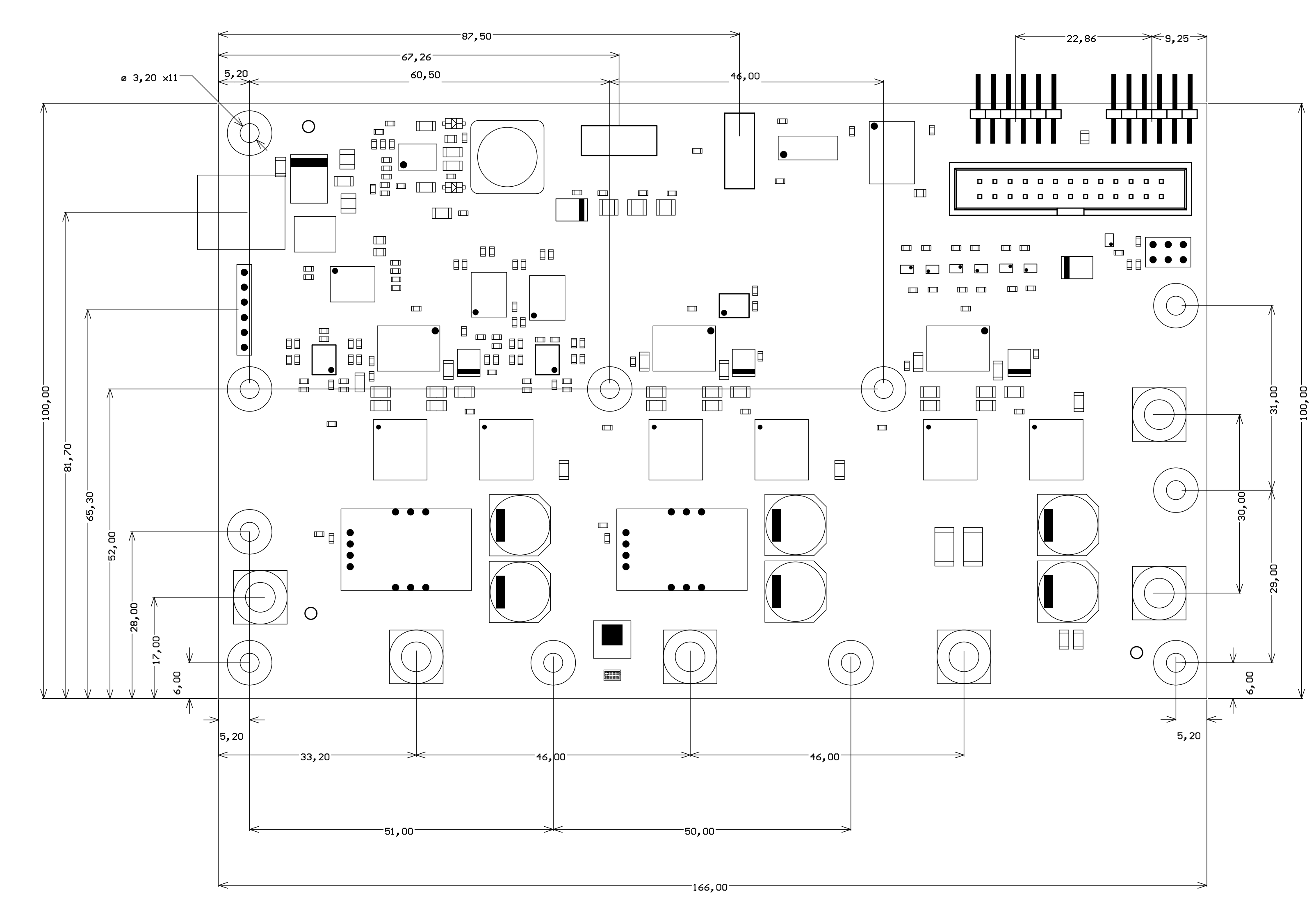
Physical Dimensions
Board size: 100 mm × 166 mm. Please download the assembly diagram for exact numbers.
PCB thickness: 1.75 mm +/-10%
Highest part on PCB: approximately 17 mm. Please download the step model for exact numbers.
All dimensions are shown in mm. Additional sketches, drawings and schematics can be found TODO: here.
Operating Temperature Ranges
Weight
| Variant | Weight in g | Note |
|---|---|---|
| - | tbd. |
|
Revision History
Hardware Revision History
| Date | Revision | Notes | PCN Link | Documentation Link |
|---|---|---|---|---|
| 2016-03-27 | 02 | TEC0053-02 |
Hardware revision number is printed on the PCB board in the down right corner.
Document Change History
Date | Revision | Authors | Description |
|---|---|---|---|
| 2017-03-30 |
| Andreas Heidemann | Initial Version |
Disclaimer
Document Warranty
...
Overview
Content Tools