Page History
...
| Signalnames | Connector J8 | Connector J9 | Connector J17 |
|---|---|---|---|
Digital Supply to EDPS | Pin 6, 12: +3.3V | Pin 6, 12: +3.3V Pin 5, 11: GND | Pin 5, 6, 21, 22: +3.3V Pin 1, 2, 25, 26: GND |
Motor Driver PWM Signals to EDPS High and Low Side control signals
| Pin 1: G1H - Ch.A HighSide | Pin 11: G1H - Ch.A HighSide | |
| ADC Clock Signal to EDPS | Pin 1: SCLK | Pin 23: SCLK | |
| Encoder Digital Signals from EDPS | Pin 8: ENC_A | Pin 20: ENC_A | |
| Motor Current ADC "raw" Signals from EDPS (usabel with FPGA IP) | Pin 2: SDI1 - Current Ch.A | Pin 19: SDI1 - Current Ch.A | |
| Supply Voltage ADC "raw" Signal from EDPS (usabel with FPGA IP) | Pin 7: SDIV - from DC_LINK | Pin 24: SDIV - from DC_LINK | |
| 1-Wire bus for temperature measurement | Pin 10: EXT1 - 1-Wire Bus 1 Pin 4: EXT2 - 1-Wire Bus 2 | Pin 4: EXT1 - 1-Wire Bus 1 | |
| Not connected pins | none | none | Pin 13, 14 |
Motor and Power Concept
There are two options available for the motor and power concept:
| Detail | Option 1: Reference Motor Board with DC +12V Supply | Option 2: Customer Motor at individual DC +5..48V | Comment | ||||
|---|---|---|---|---|---|---|---|
| Motor Supply | From DC +12V Input J7 via Fuse F3 (TODO ... A) | From customer DC Supply to J6 via F1 on Eval Boad | |||||
| Motor Connection | Motor wires connected to cage clamps on Motor Reference Board J5 (A), J4 (B), J3 (C) | Motor wires connected to bolt screw terminals on Eval Board J2 (A), J3 (B), J4 (C) | |||||
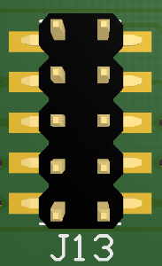
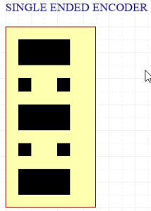
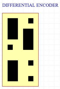
| Encoder Connection | From encoder pins via ribbon cable to Eval Board J10, 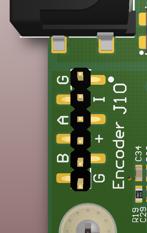 J11 single ended: | From motor to Eval Board J10 (only single ende signals) see left colomn, or to J11 (single OR differential signals):  J11 single ended: J11 differential with 100R terminated: | Jumper Settings for encoder signals.
|
|
Reference Motor Board TEC0060
...
The datasheet of the encoder:
http://www.anaheimautomation.com/manuals/accessories/L010390%20-%20Single%20Ended%20Encoder%20with%20Index%20Channel.pdf
Internal
Temperature Sensor
...
Variants Currently In Production
TODO:
Technical Specifications
Absolute Maximum Ratings
...
Weight
| Variant | Weight in g | Note |
|---|---|---|
| - | tbd.TODO |
|
Revision History
Hardware Revision History
...
Overview
Content Tools