Page History
...
| Scroll pdf ignore | |
|---|---|
Table of Contents
|
Overview
| Scroll Only (inline) |
|---|
Refer to "https://shop.trenz-electronic.de/en/Download/?path=Trenz_Electronic/TE0808" for downloadable version of this manual and the rest of available documentation. |
The Trenz Electronic TE0808 is an industrial-grade MPSoC UltraSoM integrating a Xilinx Zynq UltraScale+, 4 x 4 Gbit (256 MByte) DDR4 SDRAM with 16-Bit bit databus width, 2 x 256 MBit (32 MByte) Flash memory for configuration and operation, 20 Gigabit transceivers, and powerful switch-mode power supplies for all on-board voltages. A large number of configurable I/O's is provided via rugged high-speed stacking connections.
| Note |
|---|
Current TE0808 boards are equipped with ES1 silicon. Erratas and functional restrictions may exist, please check Xilinx documentation and contact your local Xilinx FAE for restrictions. |
Block Diagram
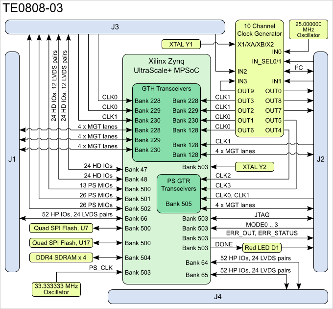
Figure 1: TE0808-03 Block Diagram
Main Components
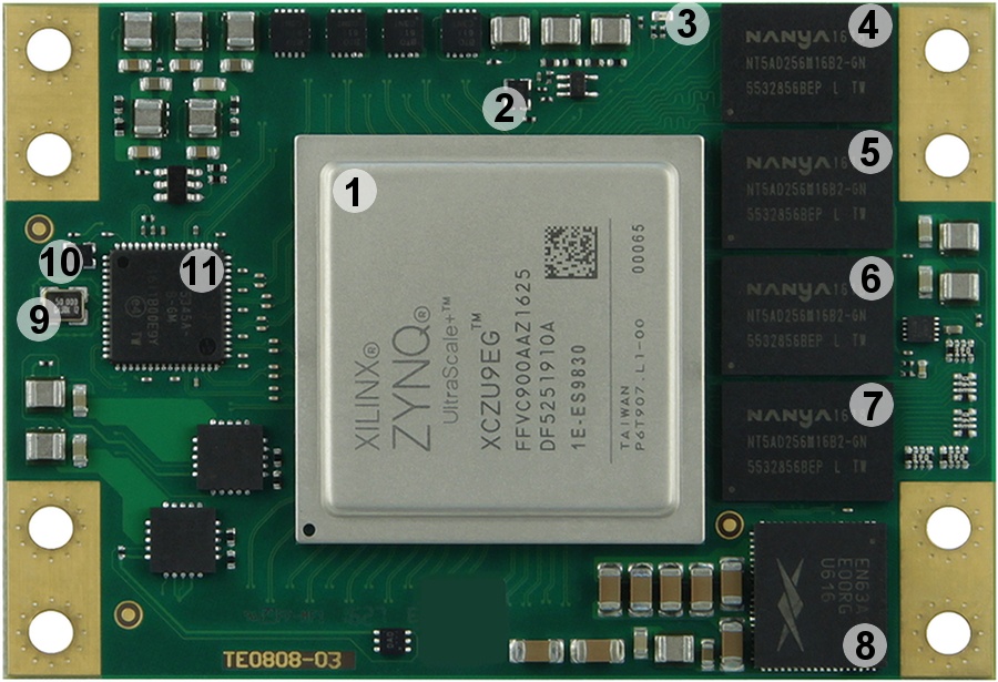

Figure 2: TE0808-03 MPSoC module
- Xilinx ZYNQ UltraScale+ XCZU9EG MPSoC, U1
- Low-power programmable oscillator @ 33.333333 MHz (PS_CLK), U32
- Red LED (DONE), D1
- 256Mx16 DDR4-2400 SDRAM, U12
- 256Mx16 DDR4-2400 SDRAM, U9
- 256Mx16 DDR4-2400 SDRAM, U2
- 256Mx16 DDR4-2400 SDRAM, U3
- 12A PowerSoC DC-DC converter, U4
- Quartz crystal, Y1
- Low-power programmable oscillator @ 25.000000 MHz (IN0 for U5), U25
- 10-channel programmable clock generator, U5
- Ultra fine 0.50 mm pitch, Razor Beam™ LP Slim Terminal Strip with 160 contacts, J4
- Ultra fine 0.50 mm pitch, Razor Beam™ LP Slim Terminal Strip with 160 contacts, J2
- Ultra fine 0.50 mm pitch, Razor Beam™ LP Slim Terminal Strip with 160 contacts, J3
- Ultra fine 0.50 mm pitch, Razor Beam™ LP Slim Terminal Strip with 160 contacts, J1
- Quartz crystal, Y2
- 256 Mbit serial NOR Flash memory, U7
- 256 Mbit serial NOR Flash memory, U17
Key Features
- MPSoC: ZYNQ UltraScale+ ZU9EG 900 pin package
- Memory
- 64-Bit DDR4, 8 GByte maximum
- Dual SPI boot Flash in parallel, 512 MByte maximum - User I/O
- 65 x MIO, 48 x HD (all), 156 x HP (3 banks)
- Serial transceiver: 4 x GTR + 16 x GTH
- Transceiver clocks inputs and outputs
- PLL clock generator inputs and outputs - Size: 52 x 76 mm, 3 mm mounting holes for skyline heat spreader
- B2B connectors: 4 x 160 pin
- Si5345 - 10 output PLL
- All power supplies on board, single 3.3V power source required
- 14 on-board DCDC regulators and 13 LDOs
- LP, FP, PL separately controlled power domains - Support for all boot modes (except NAND) and scenarios
- Support for any combination of PS connected peripherals
Initial Delivery State
| Storage device name | Content | Notes |
|---|---|---|
SPI Flash main array | Not programmed | - |
eFUSE Security | Not programmed | - |
Table 1: Initial Delivery State of the flash memories
Signals, Interfaces and Pins
Board to Board (B2B) connectors
The TE0808 MPSoC UltraSoM has four Board to Board (B2B) connectors with 160 contacts per connector.
...
| B2B connector J1 | ||||||
|---|---|---|---|---|---|---|
| Signal type | Bank / IC | Schematic names / Connector pins | Connector pin count / I/O's | VCCIO | Direction | Notes |
| GTH lane | Bank 230 (GTH) 4 GTH lanes | B230_RX3_P, B230_RX3_N, pins J1-3, J1-5 B230_RX2_P, B230_RX2_N, pins J1-9, J1-11 B230_RX1_P, B230_RX1_N, pins J1-15, J1-17 B230_RX0_P, B230_RX0_N, pins J1-21, J1-23 | 16 pins | - | Input/Output | GTH-lanes, each composed of two LVDS-pairs |
GTH lane | Bank 229 (GTH) 4 GTH lanes | B229_RX3_P, B229_RX3_N, pins J1-27, J1-29 B229_RX2_P, B229_RX2_N, pins J1-33, J1-35 B229_RX1_P, B229_RX1_N, pins J1-39, J1-41 B229_RX0_P, B229_RX0_N, pins J1-45, J1-47 | 16 pins | - | Input/Output | GTH-lanes, each composed of two LVDS-pairs |
GTH lane | Bank 228 (GTH) 4 GTH lanes | B228_RX3_P, B228_RX3_N, pins J1-27, J1-29 B228_RX2_P, B228_RX2_N, pins J1-33, J1-35 B228_RX1_P, B228_RX1_N, pins J1-39, J1-41 B228_RX0_P, B228_RX0_N, pins J1-45, J1-47 | 16 pins | - | Input/Output | GTH-lanes, each composed of two LVDS-pairs |
| LVDS pair | Bank 66 (HP) | B66_L1_P ... B66_L24_P B66_L1_N ... B66_L24_N | 48 I/O's | VCCO66 | Input/Output | VCCO max. 1.8V usable as single-ended I/O's |
| Single ended I/O | Bank 66 (HP) | B_66_T0 ... B_66_T3 pins J1-147, J1-145, J1-143, J1-141 | 4 I/O's | VCCO66 pins J1-90, J1-120 | Input/Output | VCCO max. 1.8V |
| Reference Input Voltage | Bank 66 (HP) | VREF_66, pin J1-108 | 1 pin | - | Input | - |
| Power Rail | U4 (DCDC) | PL_DCIN, pins J1-151, J1-153, J1-157, J1-159 | 4 pins | - | Input | - |
| Internal voltage level | U19 (DCDC) | PL_1V8, pins J1-91, J1-121 | 2 pins | - | Output | 1.8V nominal output |
| B2B connector J2 | ||||||
| Signal type | Bank / IC | Schematic names / Connector pins | Connector pin count / I/O's | VCCIO | Direction | Notes |
| Reference Clock signal | U5 (programmable PLL) | CLK0_P, CLK0_N, pins J2-3, J2-1 | 6 pins | - | Output | output from Si5351A-B-GM LVDS-pairs |
| Reference Clock signal | U5 (programmable PLL) | IN1_P, IN1_N, pins J2-3, J2-1 | 2 pins | - | Input | input to Si5351A-B-GM LVDS-pair |
| Reference Clock signal | Bank 505 (GTR) | B505_CLK0_P, B505_CLK0_N, pins J2-10, J2-12 B505_CLK1_P, B505_CLK1_N, pins J2-16, J2-18 | 4 pins | - | Input | reference clock input to MPSoC's bank LVDS-pairs |
| Reference Clock signal | Bank 128 (GTH) | B128_CLK1_P, B128_CLK1_N, pins J2-22, J2-24 | 2 pins | - | Input | reference clock input to MPSoC's bank LVDS-pair |
| GTH lane | Bank 128 (GTH) 4 GTH lanes | B128_RX3_N, B128_RX3_P, pins J2-28, J2-30 B128_RX2_N, B128_RX2_P, pins J2-34, J2-36 B128_RX1_N, B128_RX1_P, pins J2-40, J2-42 B128_RX0_N, B128_RX0_P, pins J2-46, J2-48 | 16 pins | - | Input/Output | GTH-lanes, each composed of two LVDS-pairs |
| GTR lane | Bank 505 (GTR) 4 GTR lanes | B505_RX3_N, B505_RX3_P, pins J2-52, J2-54 B505_RX2_N, B505_RX2_P, pins J2-58, J2-60 B505_RX1_N, B505_RX1_P, pins J2-64, J2-66 B505_RX0_N, B505_RX0_P, pins J2-70, J2-72 | 16 pins | - | Input/Output | GTR-lanes, each composed of two LVDS-pairs |
| Control line | Bank 503 (PSCONFIG) | DONE, pin J2-116 (indicated by red LED D1) | 11 I/O's | PS_1.8V | Input/Output | - |
| JTAG Interface | Bank 503 (PSCONFIG) | TCK, pin J2-120 | 4 I/O's | PS_1.8V | Input/Output | - |
| Analog input differential pair | MPSoC ADC | V_P, V_N, pins J2-113, J2-115 DX_P, DX_N, pins J2-119, J2-121
| 4 pins | - | Input/Output | LVDS-pairs |
| Control line | U5 (programmable PLL) | PLL_FINC, pin J2-81 | 8 I/O's | 1.8V | Input/Output | Control interface to Si5351A-B-GM |
| Control line | U44 (DCDC) U10 (DCDC) | EN_PSGT, pin J2-84 | 2 I/O's | EN_PSGT: max. 'DCDCIN', PG_PSGT: extern pull-up needed, max. 6V | Input/Output | "Enable"- and corresponding "Power Good"-Signal |
| Control line | U39 (DCDC) U30 (DCDC) | EN_FPD, pin J2-102 PG_FPD, pin J2-110 | 2 I/O's | EN_FPD: max. 'DCDCIN', PG_FPD: pulled-up to 'DCDCIN' | Input/Output | "Enable"- and corresponding |
| Control line | U29 (DCDC) | EN_LPD, pin J2-108 | 2 I/O's | EN_LPD: max. 7V, LP_GOOD: pulled-up to 'LP_DCDC' | Input/Output | "Enable"- and corresponding |
| Control line | U40 (DCDC) | EN_DDR, pin J2-112 | 2 I/O's | EN_DDR: max. 'DCDCIN', PG_DDR: pulled-up to 'DCDCIN' | Input/Output | "Enable"- and corresponding |
| Control line | U38 (DCDC) U38 (DCDC) | EN_PLL_PWR, pin J2-77 | 2 I/O's | EN_PLL_PWR: max. 7V, PG_PLL_1V8: extern pull-up needed, max. 6V | Input/Output | "Enable"- and corresponding |
| Control line | U43 (DCDC) U13 (DCDC) | EN_GT_L, pin J2-79 | 2 I/O's | EN_GT_L: max. 'GT_DCDC', PG_GT_L: extern pull-up needed, max. 6V | Input/Output | "Enable"- and corresponding |
| Control line | U42 (DCDC) U28 (DCDC) | EN_GT_R, pin J2-95 | 2 I/O's | EN_GT_R: max. 'GT_DCDC', PG_GT_R: extern pull-up needed, max. 6V | Input/Output | "Enable"- and corresponding |
| Control line | U4 (DCDC) U19 (DCDC) | EN_PL, pin J2-101 | 2 I/O's | EN_PL connected to 'PL_DCIN' | Input/Output | "Enable"- and corresponding |
| Control line | U41 (voltage monitor IC) | MR, pin J2-83 | 1 I/O | max. 'LP_DCDC' | Input | Manual-reset (low-active signal). Leave unconnected or connect |
| Power Rail | U24/U31/U30/U23 (DCDC) | DCDCIN pins J2-154, J2-156, J2-158, J2-160, J2-153, J2-155, J2-157, J2-159 | 8 pins | - | Input | - |
| Power Rail | U20/U41 (DCDC) | LP_DCDC, pins J2-138, J2-140, J2-142, J2-144 | 4 pins | - | Input | - |
| Power Rail | Bank 503 (PSCONFIG) | PS_BATT, pin J2-125 | 1 pin | - | Input | - |
| Internal voltage level | U15 (DCDC) | PS_1V8, pin J2-99 | 1 pin | - | Output | 1.8V nominal output |
| Internal voltage level | U31 (DCDC) | DDR_1V2, pin J2-135 | 1 pin | - | Output | 1.2V nominal output |
| B2B Connector J3 | ||||||
| Signal type | Bank / IC | Schematic names / Connector pins | Connector pin count / I/O's | VCCIO | Direction | Notes |
| LVDS pair | Bank 48 (HD) | B48_L1_P ... B48_L12_P | 24 I/O's | VCCO48 | Input/Output | VCCO max. 3.3V |
| LVDS pair | Bank 47 (HD) | B47_L1_P ... B47_L12_P | 24 I/O's | VCCO47 | Input/Output | VCCO max. 3.3V |
| Reference Clock signal | U5 (programmable PLL) | IN2_P, IN2_N, pins J3-66, J3-68 | 2 pins | - | Input | input to Si5351A-B-GM LVDS-pair |
| Reference Clock signal | Bank 228 (GTH) | B228_CLK0_P, B228_CLK0_N, pins J3-10, J3-12 | 2 pins | - | Input | reference clock input to MPSoC's bank LVDS-pairs |
| Reference Clock signal | Bank 229 (GTH) | B229_CLK0_P, B229_CLK0_N, pins J3-22, J3-24 | 2 pins | - | Input | reference clock input to MPSoC's bank LVDS-pairs |
| Reference Clock signal | Bank 230 (GTH) | B230_CLK1_P, B230_CLK1_N, pins J3-10, J3-12 | 2 pins | - | Input | reference clock input to MPSoC's bank LVDS-pairs |
| MIO | Bank 500 (PSMIO) | MIO13 ... MIO25 | 13 I/O's | PS_1V8 | Input/Output | - |
| MIO | Bank 501 (PSMIO) | MIO26 ... MIO51 | 26 I/O's | PS_1V8 | Input/Output | - |
| MIO | Bank 502 (PSMIO) | MIO52 ... MIO77 | 26 I/O's | PS_1V8 | Input/Output | - |
| Power Rail | U38/U35/U36/U21/U22 (DCDC) | GT_DCDC, pins J3-157, J3-158, J3-159, J3-160 | 4 pin | - | Input | - |
| Power Rail | U5 (programmable PLL) | PLL_3V3, pin J3-152 | 1 pin | - | Input | 3.3V nominal input |
| Internal voltage level | U38 (DCDC) | SI_PLL_1V8, pin J3-151 | 1 pin | - | Output | 1.8V nominal output |
| Internal voltage level | U15 (DCDC) | PS_1V8, pins J3-147, J3-148 | 2 pins | - | Output | 1.8V nominal output |
| B2B Connector J4 | ||||||
| Signal type | Bank / IC | Schematic names / Connector pins | Connector pin count / I/O's | VCCIO | Direction | Notes |
| LVDS pair | Bank 64 (HP) | B64_L1_P ... B64_L24_P | 48 I/O's | VCCO64 | Input/Output | VCCO max. 1.8V |
| LVDS pair | Bank 65 (HP) | B65_L1_P ... B65_L24_P | 48 I/O's | VCCO65 | Input/Output | VCCO max. 1.8V |
| Single ended I/O | Bank 64 (HP) | B_64_T0 ... B_64_T3 | 4 I/O's | VCCO64 | Input/Output | VCCO max. 1.8V |
| Single ended I/O | Bank 65 (HP) | B_65_T0 ... B_65_T3 | 4 I/O's | VCCO65 | Input/Output | VCCO max. 1.8V |
Reference Input Voltage | Bank 64 (HP) | VREF_64, pin J4-88 | 1 pin | - | Input | - |
| Reference Input Voltage | Bank 65 (HP) | VREF_65, pin J4-15 | 1 pin | - | Input | - |
...
For detailed information about the B2B pin-out, please refer to the Pin-out table.
Quad-SPI Flash memory
The TE0808-03 UltraSoM is equipped with two Micron Serial NOR Flash Memory with 256 Mbit (32 Mbyte) storage capacity each. The flash memory ICs with the schematic designators U7 and U17 are connected to bank 500 (PSMIO) of the Zynq MPSoC module via QSPI interface.
...
Table 3: Flash memory QSPI-interface
DDR4-2400 SDRAM
The TE0808-03 UltraSoM is equipped with with four Nanya NT5AD256M16B2-GN DDR4-2400 SDRAM modules with 4 Gbit (256 MByte) memory density. The SDRAM modules are connected to the PS DDR controller (bank 504) with 16 bit databus width respectively.
LEDs
TE0808 has one red LED (D1) which reflects MPSoC's 'DONE' signal. This LED goes ON when power has been applied to the module and stays ON until MPSoC's programmable logic is configured properly.
Clocking
Programmable Clock Generator
Following table illustrates on-board Si5345A programmable clock multiplier chip inputs and outputs:
...
| Clock | Frequency | FPGA Pin | Connected To |
|---|---|---|---|
| PS_CLK | 33.333333 MHz | P20 | MEMS Oscillator |
| PS_PAD (RTC) | 32.768 kHz | R22/R23 | Quartz crystal |
Power and Power-On Sequence
The TE0808-03 module with the Xilinx Zynq Ultrascale+ MPSoC delivers a heterogeneous multi-processing system with integrated programmable logic and independently operable elements and is designed to meet embedded system power management requirement by advanced power management features. This features allow to offset the power and heat constraints against overall performance and operational efficiency.
...
Figure 3: TE0808-03 Power-On sequence diagram
B2B connectors
| Include Page | ||||
|---|---|---|---|---|
|
Technical Specifications
Absolute Maximum Ratings
Parameter | Min | Max | Unit | Notes / Reference Document |
|---|---|---|---|---|
| PL_DCIN | -0.3 | 7 | V | TPS82085SIL/EN63A0QI data sheet |
| DCDCIN | -0.3 | 7 | V | TPS82085SIL/TPS51206PSQ data sheet |
| LP_DCDC | -0.3 | 4 | V | TPS3106K33DBVR data sheet |
| GT_DCDC | -0.3 | 7 | V | TPS82085SIL data sheet |
| PS_BATT | -0.5 | 2 | V | Xilinx DS925 data sheet |
| PLL_3V3 | -0.5 | 3.8 | V | Si5345/44/42 data sheet |
| VCCO for HD I/O banks | -0.5 | 3.4 | V | Xilinx DS925 data sheet |
| VCCO for HP I/O banks | -0.5 | 2 | V | Xilinx DS925 data sheet |
| VREF | -0.5 | 2 | V | Xilinx DS925 data sheet |
| I/O input voltage for HD I/O banks | -0.55 | VCCO + 0.55 | V | Xilinx DS925 data sheet |
| I/O input voltage for HP I/O banks | -0.55 | VCCO + 0.55 | V | Xilinx DS925 data sheet |
| PS I/O input voltage (MIO pins) | -0.5 | VCCO_PSIO + 0.55 | V | Xilinx DS925 data sheet, VCCO_PSIO 1.8V nominally |
Receiver (RXP/RXN) and transmitter | -0.5 | 1.2 | V | Xilinx DS925 data sheet |
Voltage on input pins of | -0.5 | VCC + 0.5 | V | NC7S08P5X data sheet, see schematic for VCC |
Voltage on input pins (nMR) of | -0.3 | VDD + 0.3 | V | TPS3106 data sheet, |
| "Enable"-signals on TPS82085SIL ('EN_PLL_PWR', 'EN_LPD') | -0.3 | 7 | V | TPS82085SIL data sheet |
Storage temperature (ambient) | –40 | 125 | °C | TPS82085SIL data sheet |
Recommended Operating Conditions
| Parameter | Min | Max | Unit | Notes / Reference Document |
|---|---|---|---|---|
| PL_DCIN | 1.8 | 6 | V | TPS82085SIL data sheet |
| DCDCIN | 3.1 | 6 | V | TPS82085SIL/TPS51206PSQ data sheet |
| LP_DCDC | 2.0 | 3.6 | V | TPS3106K33DBVR data sheet |
| GT_DCDC | 1.8 | 6 | V | TPS82085SIL data sheet |
| PS_BATT | 1.2 | 1.5 | V | Xilinx DS925 data sheet |
| PLL_3V3 | 3.14 | 3.47 | V | Si5345/44/42 data sheet 3.3V typical |
| VCCO for HD I/O banks | 1.14 | 3.4 | V | Xilinx DS925 data sheet |
| VCCO for HP I/O banks | 0.95 | 1.9 | V | Xilinx DS925 data sheet |
| I/O input voltage for HD I/O banks. | -0.2 | VCCO + 0.2 | V | Xilinx DS925 data sheet |
| I/O input voltage for HP I/O banks | -0.2 | VCCO + 0.2 | V | Xilinx DS925 data sheet |
| PS I/O input voltage (MIO pins) | -0.2 | VCCO_PSIO + 0.2 | V | Xilinx DS925 data sheet, VCCO_PSIO 1.8V nominally |
| Voltage on input pins of NC7S08P5X 2-Input AND Gate | 0 | VCC | V | NC7S08P5X data sheet, |
Voltage on input pins (nMR) of | 0 | VDD | V | TPS3106 data sheet, |
| Note |
|---|
| Assembly variants for higher storage temperature range are available on request. |
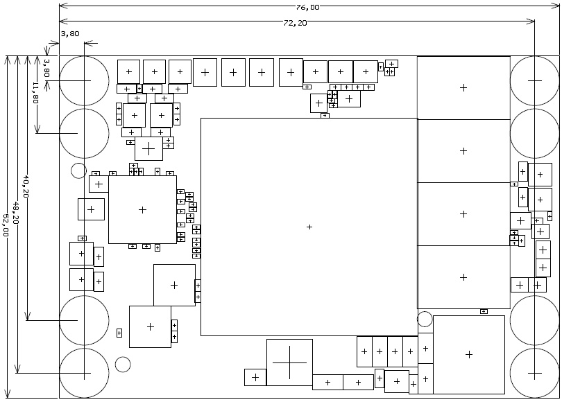
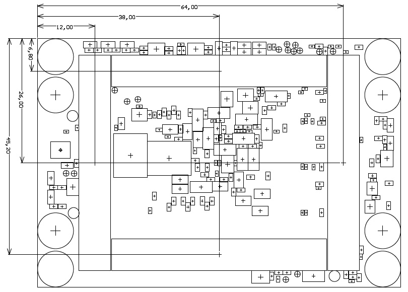
Physical Dimensions
Module size: 52 mm × 76 mm. Please download the assembly diagram for exact numbers
Mating height with standard connectors: 4mm
PCB thickness: 1.6mm
Highest part on PCB: approx. 3mm. Please download the step model for exact numbers
All dimensions are given in millimeters.
Operating Temperature Ranges
Commercial grade: 0°C to +70°C.
...
The module operating temperature range depends also on customer design and cooling solution. Please contact us for options.
Weight
17 g - Plain module
Revision History
Hardware Revision History
| Date | Revision | Notes | Link to PCN | Documentation Link |
|---|---|---|---|---|
| - | 03 | Second production release | - | TE0808-03 |
| 2016-03-09 | 02 | First production release | - | TE0808-02 |
| - | 01 | Prototypes | - | - |
Hardware revision number is written on the PCB board together with the module model number separated by the dash.

Document Change History
| Date | Revision | Contributors | Description |
|---|---|---|---|
| 2017-02-06 | Jan Kumann | Initial document. |
Disclaimer
| Include Page | ||||
|---|---|---|---|---|
|
Overview
Content Tools