Page History
...
| Scroll Only (inline) |
|---|
Refer to https://shopwiki.trenz-electronic.de/de/Download/?path=Trenz_Electronicdisplay/PD/TE0713+TRM for the downloadableonline version of this manual and the rest of available documentation. |
Trenz Electronic TE0713 is an industrial-grade FPGA module integrating Xilinx Artix-7 FPGA, USB 3.0 to FIFO bridge, 1 GByte of DDR3L SDRAM, 32 MByte Flash memory for configuration and operation, and powerful switching-mode power supplies for all on-board voltages. Numerous configurable I/Os are provided via rugged high-speed strips. All this on a tiny footprint, smaller than a credit card size at very competitive price. All Trenz Electronic SoMs in 4 x 5 cm form factor are mechanically compatible.
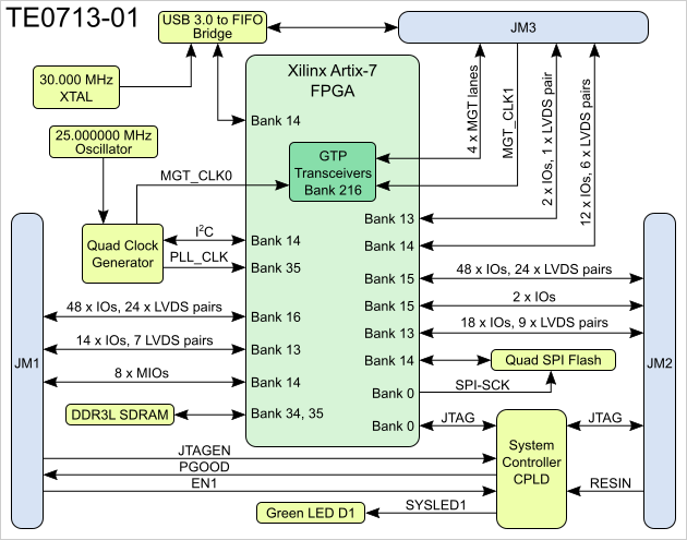
Block Diagram
Main Components

...
.
...
Key Features
- Xilinx Artix-7 (15T to 200T) SoM (System on Module)series FPGA
- Both industrial and commercial temperature ranges available
- Rugged for high shock and high vibration resistance
- 1 GByte DDR3L 32-bit SDRAM
- 32 MByte QSPI Flash memory (with XiP support)
- USB 3.0 to FIFO interface bridge
- Programmable clock quad generator
- GTP transceiver clock (default 125 MHz)
- Fabric clock (default 200 MHz)
- GTP transceiver clock (default 125 MHz)
- Plug-on module with 2 × 100-pin and 1 × 60-pin high-speed hermaphroditic strips
- 152 FPGA I/Os (75 differential pairs) available via B2B connectors
- 4 GTP (multi Gigabit transceiver) lanes
- External clock input for GTP transceivers via B2B connector
- On-board high-efficiency DC-DC converters
- System management and power sequencing
- eFUSE bit-stream encryption
- AES bit-stream encryption
- User configurable LED
Evenly-spread supply pins for good signal integrity
Additional assembly options are available for cost or performance optimization upon request.
Block Diagram
| Page break |
|---|
Main Components
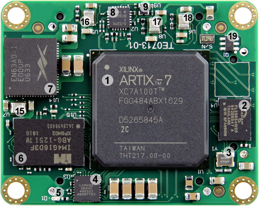
- Xilinx Artix-7 XC7A series FPGA, U1
- 32 MByte QSPI Flash memory, U4
- 30.000 MHz quartz crystal, Y1
- System Controller CPLD, Lattice Semiconductor MachXO2-256HC, U3
- Green LED (SYSLED1), D1
- 4 Gbit DDR3L 256M x 16 SDRAM, U15
- Altera Enpirion 12A PowerSoC DC-DC converter, U14
- Silicon Labs programmable quad clock generator, U2
- SiTime low-power programmable oscillator @ 25.000000 MHz, U9
- 4 Gbit DDR3L 256M x 16 SDRAM, U19
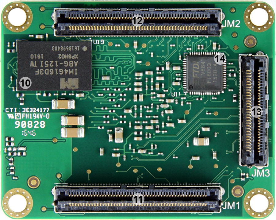
- Samtec Razor Beam™ LSHM-150 B2B connector, JM1
- Samtec Razor Beam™ LSHM-150 B2B connector, JM2
- Samtec Razor Beam™ LSHM-130 B2B connector, JM3
- FTDI USB 3.0 to FIFO interface bridge, U11
- Texas Instruments 3A step-down converter (DDR_PWR), U7
- Texas Instruments 3A step-down converter (1.8V), U5
- Texas Instruments 3A step-down converter (1.2V_MGT), U8
- Texas Instruments 3A step-down converter (1V_MGT), U6
- Texas Instruments PFET load switch, Q1
Initial Delivery State
Programmable unit | Content | Notes |
|---|---|---|
| Xilinx Artix-7 FPGA | Not programmed | U1 |
| System Controller CPLD | Programmed | U3 |
| SPI Flash OTP area | Empty | U4 |
SPI Flash main array | Empty | U4 |
| SPI Flash Quad Enable bit | Set | U4 |
...
JTAGEN pin in B2B connector JM1 is used to select JTAG access for FPGA or SC System Controller CPLD:
| JTAGEN | JTAG Access To |
|---|---|
| Low | Artix-7 FPGA |
| High | System Controller CPLD |
| Page break |
|---|
System Controller I/O Pins
...
| Pin Name | Mode | Function | Default Configuration |
|---|---|---|---|
| PGOOD | Output | Power good | Active high when all on-module power supplies are working properly. |
| JTAGEN | Input | JTAG select | Low for normal operation, high for System Controller CPLD access. |
| EN1 | Input | Power Enable | When forced low, pulls POR_B low to emulate power on reset. |
| NOSEQ | - | No function | Not used. |
| MODE | - | No function | Not used. |
On-board LEDs
The TE0713-01 module has one LED which is connected to the System Controller CPLD. Once FPGA configuration has completed, it can be used by the user's design.
...
On-board Si5338 clock generator chip is used to generate clocks with 25 MHz oscillator connected to the pin IN3 as input reference. There is a I2C I2C bus connection between the FPGA bank 14 (master) and clock generator chip (slave) which can be used to program output frequencies. See the reference design for more information.
...
System Controller CPLD (Lattice Semiconductor MachXO2-256HC, U3) is used to control FPGA configuration process. The FPGA is held in reset (by driving the PROG_B signal low) until all power supplies have stabilized.
...
User can create their own System Controller design using Lattice Diamond software. Once created it can be programmed into CPLD via JTAG interface.
...
DDR3L SDRAM
The TE0713-01 SoM has two 4 Gbit volatile DDR3 SDRAM ICs (U15 and U19) for storing user application code and data.
...
See Xilinx datasheet DS181 - "Artix-7 FPGAs Data Sheet: DC and AC Switching Characteristics" for additional information. User should also check related baseboard documentation when choosing baseboard design for TE0713 module.
| Page break |
|---|
Power Rails
Power Rail Name | B2B Connector JM1 Pin | B2B Connector JM2 Pin | Direction | Notes |
|---|---|---|---|---|
VIN | 1, 3, 5 | 2, 4, 6, 8 | Input | SoM supply voltage (from the baseboard). |
| 3.3VIN | 13, 15 | - | Input | SoM supply voltage (from the baseboard). |
| DDR_PWR | - | 19 | Output | Module internal supply of 1.35V level. |
| 1V | - | - | - | Module internal supply of 1V level. |
| 1V_MGT | - | - | - | Module internal supply of 1V for bank 216 transceivers. |
| 1.2V_MGT | - | - | - | Module internal supply of 1.2V for bank 216 transceivers. |
1.8V | 39 | - | Output | Module internal 1.8V level. Maximum 300mA available. |
| 3.3V | - | 10, 12 | Output | Module internal 3.3V level. |
| VCCIO13 | - | 1, 3 | Input | High-Range bank supply voltage (from the baseboard). |
| VCCIO15 | - | 7, 9 | Input | High-Range bank supply voltage (from the baseboard). |
| VCCIO16 | 9, 11 | - | Input | High-Range bank supply voltage (from the baseboard). |
| VREF_JTAG | - | 91 | Output | JTAG reference voltage (3.3V). |
Board to Board Connectors
| Include Page | ||||
|---|---|---|---|---|
|
Variants Currently In Production
Module Variant | FPGA | Junction Temperature | Temperature Range |
|---|---|---|---|
| TE0713-01-100-2C | XC7A100T-2FGG484C | 0°C to 85°C | Commercial grade |
| TE0713-01-200-2C | XC7A200T-2FBG484C | 0°C to 85°C | Commercial grade |
Technical Specifications
Absolute Maximum Ratings
Parameter | Min | Max | Units | Reference Document |
|---|---|---|---|---|
VIN supply voltage |
| -0.3 | 7.0 | V |
| See EN63A0QI and TPS82085 datasheets. |
| 3.3VIN supply |
| voltage | -0.5 | 3.75 | V | See LCMXO2-256HC datasheet. |
| HR I/O banks supply voltage (VCCO) | -0.5 | 3.6 | V | Xilinx datasheet DS181 |
| HR I/O banks input voltage | -0.4 | VCCO + 0.55 | V | Xilinx datasheet DS181 |
| GTP transceivers Tx/Rx input voltage | -0.5 | 1.26 | V | Xilinx datasheet DS181 |
Storage temperature | -55 | 100 | °C |
| See IM4G16D3FABG datasheet. |
Recommended Operating Conditions
| Parameter | Min | Max | Units | Reference Document |
|---|---|---|---|---|
| VIN supply voltage |
| 2.5 | 6.0 | V |
| See TPS82085 datasheet. |
| 3.3VIN supply |
| voltage | 2.375 | 3.6 | V | See LCMXO2-256HC datasheet. |
| HR I/O banks supply voltage (VCCO) | 1.14 | 3.465 | V | Xilinx datasheet DS181 |
| HR I/O banks input voltage | -0.20 | VCCO + 0.2 | V | Xilinx datasheet DS181 |
Operating Temperature Ranges
Commercial grade: 0°C to +70°C.
Industrial grade: -40°C to +85°C.
Operating temperature range depends also on customer design and cooling solution. Please contact us for options.
| Note |
|---|
| Assembly variants for higher storage temperature range are available on request. |
| Page break |
|---|
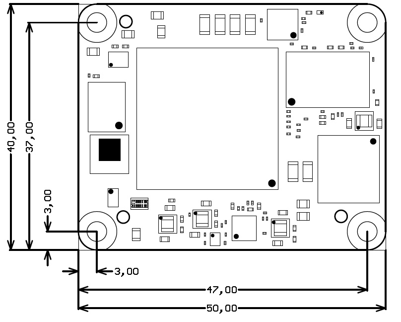
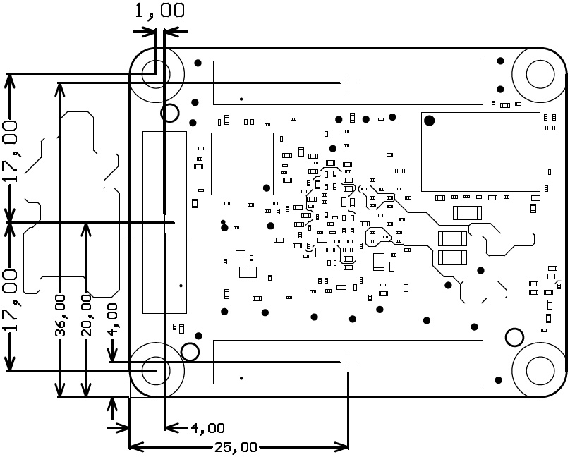
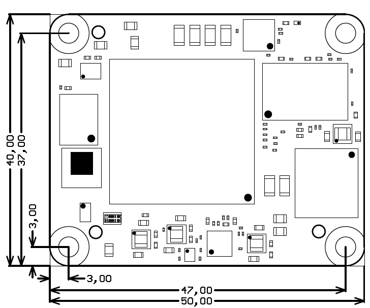
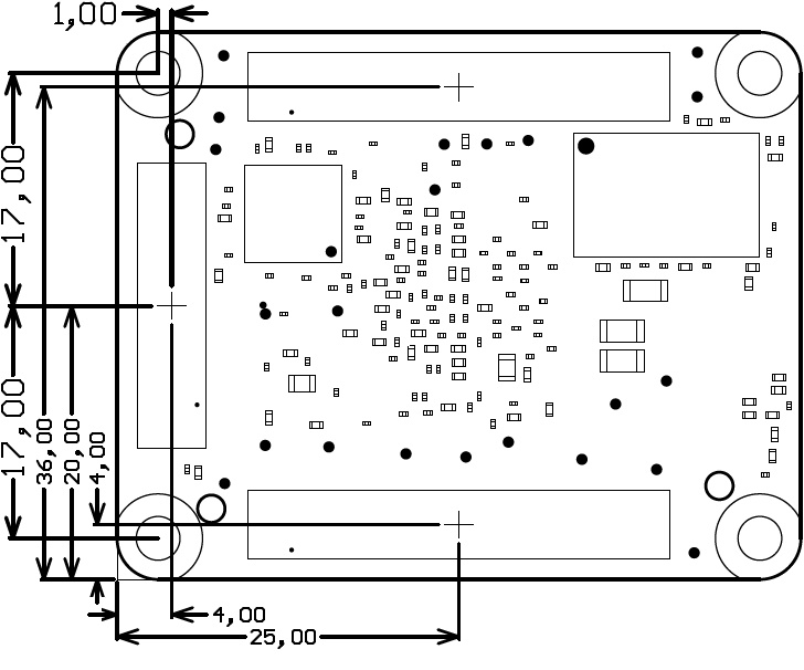
Physical Dimensions
- Module size: 50 mm × 40 mm. Please download the assembly diagram for exact numbers.
- Mating height with standard connectors: 8mm
- PCB thickness: 1.6mm
- Highest part on PCB: approx. 2.5mm. Please download the step model for exact numbers.
All dimensions are shown in millimeters.
Operating Temperature Ranges
Commercial grade: 0°C to +70°C.
Industrial grade: -40°C to +85°C.
Operating temperature range depends also on customer design and cooling solution. Please contact us for options.
Weight
21 g Plain module.
8.8 g Set of nuts and bolts.
...
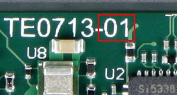
Hardware revision number is printed on the PCB board together with the module model number separated by the dash.
Document Change History
Date | Revision | Contributors | Description |
|---|---|---|---|
| 2017-05-28 | Jan Kumann | Absolute and recommended ratings added. Main components section improved. New top PCB image. Power rails section improved. New physical dimensions images. | |
| 2017-02-07 | V1 | Jan Kumann | Initial document. |
Disclaimer
| Include Page | ||||
|---|---|---|---|---|
|
Overview
Content Tools