some sources available on public doc TEBT0808 TRM
| Page properties |
|---|
|
Template Revision 2.5
- Module: TRM Name always "TE Series Name" +TRM
Example: "TE0728 TRM" - Carrier: TRM Name usually "TEB Series Name" +TRM
Example: "TEB0728 TRM"
|
...
| Page properties |
|---|
|
Note for Download Link of the Scroll ignore macro: |
| Scroll pdf ignore |
|---|
Table of Contents |
...
The Trenz Electronic TEBT0808 -01 is a testboard test fixture for module TE0808(REV 02 and 03) as well as for TE0803 (REV 01)REV02, REV03) and TE0803(REV01) series.
Refer to http://trenz.org/tebt0808-info for the current online version of this manual and other available documentation.
...
- Modules
- On Board
- Done/Error/Status LEDs
- MEMS Oscillator 125.00 MHz
- Boot Mode DIP-Switch
- 2x DIP-Switches to control TE080x power domains
- Interface
- Accepts TE0808 / TE0803
- Single 3.3V input
- Header for TE0790 JTAG/UART Adapter
20 Pin (connected to MIO JTAG 0)- 10 Pin I2C header for Silabs Clock Builder Field Programmer
- Pin Header for I2C
- Board to Board (B2B) Connectors
Done, Error/Status LEDs connectors SMA connectors- GT local loopback
- PL I/O loopbacks
- PS I/O loopbacks
- Boot Mode switches
- Power control switches to control TE0808 power domains
- 4x SMA Connectors
- One pre-assembled TE0790 XMOD FTDI JTAG adapter
Supported Bootmodes are SPI and JTAG.
- Power:
- 3.3 V (Nominal Supply Voltage)
- Dimension: 90mm x 90mm
Block Diagram
| Page properties |
|---|
|
add drawIO object here.
|
...
| Scroll Title |
|---|
| anchor | Figure_OV_BD |
|---|
| title | TEBT0808 block diagramBlock Diagram |
|---|
|
| Scroll Ignore |
|---|
| draw.io Diagram |
|---|
| border | truefalse |
|---|
| viewerToolbar | true |
|---|
| |
|---|
| fitWindow | false |
|---|
| diagramDisplayName | |
|---|
| lbox | true |
|---|
| revision | 23 |
|---|
| diagramName | TEBT0808_OV_BD |
|---|
| simpleViewer | false |
|---|
| width |
|---|
| diagramWidth | 635 |
|---|
| | links | auto |
|---|
| tbstyle | hidden |
|---|
| diagramWidth | 636 | revision | 6 |
|---|
|
|
| Scroll Only |
|---|
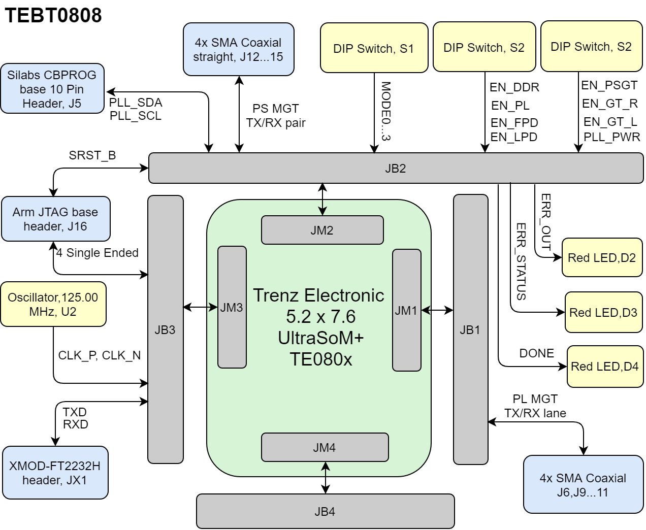 Image Modified Image Modified
|
|
Main Components
...
| Scroll Title |
|---|
| anchor | Figure_OV_BD |
|---|
| title | TEBT0808 main componentsMain Components |
|---|
|
| Scroll Ignore |
|---|
| draw.io Diagram |
|---|
| border | truefalse |
|---|
| viewerToolbar | true |
|---|
| |
|---|
| fitWindow | false |
|---|
| diagramDisplayName | |
|---|
| lbox | true |
|---|
| revision | 4 |
|---|
| diagramName | TEBT0808_OV_MC |
|---|
| simpleViewer | false |
|---|
| width | |
|---|
| links | auto |
|---|
| tbstyle | hidden |
|---|
| diagramWidth | 640 |
|---|
| revision | 3 |
|---|
|
|
| Scroll Only |
|---|
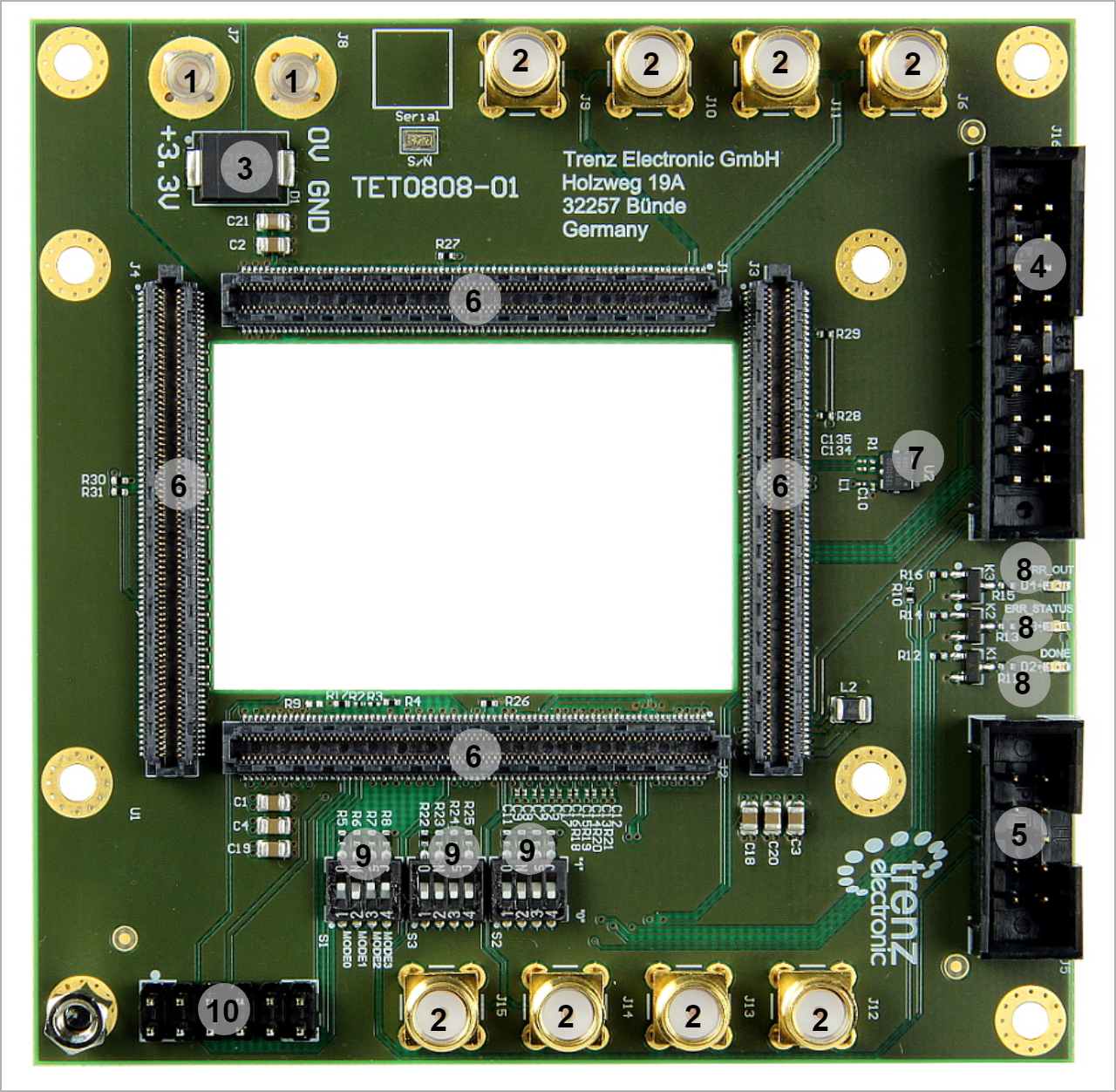 Image Modified Image Modified
|
|
- Uninsulated 2 mm rigid socket. J8-J7Power Jack. J7-J8
- SMA Coaxial straight. J6- J9...15
- Surface Mount Schottky Barrier Rectifier. D1
- ARM PJTAG Pin Header J16
- I2C Pin Header, J5Box Headers, Straight/Angled J5-J16
- Board to Board ConnectorConnectors. J1...4
- Clock MEMS Oscillator, U2
- On-Board LEDLEDs, D1D2...34
- DIP-Switch, S1...3
- XMOD JTAG Baseheader, JX1
Initial Delivery State
| Page properties |
|---|
|
Notes : Only components like EEPROM, QSPI flash and DDR3 can be initialized by default at manufacture. If there is no components which might have initial data ( possible on carrier) you must keep the table empty |
...
| Scroll Title |
|---|
| anchor | Table_OV_IDS |
|---|
| title | Initial delivery state of programmable devices on the module |
|---|
|
| Scroll Table Layout |
|---|
| orientation | portrait |
|---|
| sortDirection | ASC |
|---|
| repeatTableHeaders | default |
|---|
| style | |
|---|
| widths | |
|---|
| sortByColumn | 1 |
|---|
| sortEnabled | false |
|---|
| cellHighlighting | true |
|---|
|
Storage device name | Content | Notes |
|---|
- | - | - |
|
Configuration Signals
| Page properties |
|---|
|
- Overview of Boot Mode, Reset, Enables.
|
...
| Scroll Title |
|---|
| anchor | Table_OV_BP |
|---|
| title | Boot processProcess. |
|---|
|
| Scroll Table Layout |
|---|
| orientation | portrait |
|---|
| sortDirection | ASC |
|---|
| repeatTableHeaders | default |
|---|
| style | |
|---|
| widths | |
|---|
| sortByColumn | 1 |
|---|
| sortEnabled | false |
|---|
| cellHighlighting | true |
|---|
|
Hex0x0| 0b0000 | PS Main JTAG (TE0790 USB JTAG) |
Needed for SPI Flash Programming| DIPs are inverted | | ON | ON | OFF | ON |
0x2| 0b0010 | SPI Flash (dual parallel, 4bit x 2, 32bit Addressing) |
Default | | DIPs are inverted | | OFF | ON | ON | ON | 0b1000 | PJTAG(MIO29:26) | DIPs are inverted |
|
| Scroll Title |
|---|
| anchor | Table_OV_RST |
|---|
| title | Reset Process. |
|---|
|
|
| Scroll Title |
|---|
| anchor | Table_OV_RST |
|---|
| title | Reset process. |
|---|
|
| scroll-tablelayout |
|---|
| orientation | portrait |
|---|
| sortDirection | ASC |
|---|
| repeatTableHeaders | default |
|---|
| style | |
|---|
| widths | |
|---|
| sortByColumn | 1 |
|---|
| sortEnabled | false |
|---|
| cellHighlighting | true |
|---|
|
Signal | B2B | Note |
|---|
PLL_RST | J2-89 |
| | SRST_B | J2-96 | connected Connected to PJTAG0_SRST - J16 |
|
Signals, Interfaces and Pins
...
Board to Board (B2B) I/Os
FPGA bank number and number TEBT0808 has four B2B Connectors and each connector has 160 pins. Number of I/O signals and Interfaces connected to the B2B connectorconnectors is as following table:
| Scroll Title |
|---|
| anchor | Table_SIP_B2B |
|---|
| title | General PL I/O to B2B connectors information |
|---|
|
| Scroll Table Layout |
|---|
| orientation | portrait |
|---|
| sortDirection | ASC |
|---|
| repeatTableHeaders | default |
|---|
| style | |
|---|
| widths | |
|---|
| sortByColumn | 1 |
|---|
| sortEnabled | false |
|---|
| cellHighlighting | true |
|---|
|
| B2B Connector | Interfaces | Number of I/O | Notes |
|---|
J1
| User I/O |
22 singel ended, 11 46 Single Ended, 23 Differential |
8 singel ended, 4 16 Single Ended, 8 Differential |
8 singel ended, 4 16 Single Ended, 8 Differential |
8 singel ended, 4 Differential 3 singel ended Connected to Bank 66 Connected to Bank 228 Connected to Bank 229 Connected to Bank 230 VCCO_66, 16 Single Ended, 8 Differential 4 Single Ended | IOs are Loop-Back IOs are Loop-Back IOs are Loop-Back IOs are Loop-Back |
Ethernet PHY | 32 singel ended, 16 Differential 4 singel ended, 16 Differential | Connected to Bank 505 Connected to Bank 128 | Control Signals |
| User IO | 28 Single Ended, 14 Differential 6 Single Ended, 3 Differential | IOs are Loop-Back IOs are Loop-Back | | Boot Mode | 4 Single Ended | MODE0...3 | | Control Signals | 25 Single Ended |
15 single ended | PLL_SEL0, PLL_SEL1, PLL_RST, EN_GTR, EN_PL, PLL_LOLN, EN_PSGT, ERR_STATUS, ERR_OUT,SRST_B, INIT_B, PROG_B, EN_FPD , EN_LPD , DONE |
Power Control Signal | 10 single ended | , EN_PLL_PWR, PLL_FINC ,PG_PLL_1V8, LP_GOOD, PG_DDR, PG_PL, PG_FPD, PG_PSGT, PG_GT_R, PG_GT_L | | JTAG Interface | 7 |
single ended| Single Ended | TCK, TDI, TMS, TDO, MR, Rxd, Txd |
WANNE2 single ended| Single Ended | PLL_SCL, PLL_SDA | | Clock | 6 |
singel endedSingle Ended, 3 Differential | CLK0, CLK7, CLK8 | J3
| User |
I/O12 singel ended, 6 Differential 12 singel ended, 6 | IO | 24 Single Ended, 12 Differential 24 Single Ended, 12 Differential | Connected to Module FPGA, Bank 48 Connected to Module FPGA, Bank 47 | | Clock | 6 |
singel ended| Single Ended, 3 Differential | CLK228, CLK229, CLK230 | | PJTAG Interface |
7 single ended| 4 Single Ended | PJTAG0_TCK, PJTAG0_TDI, PJTAG0_TMS, PJTAG0_TDO, | | MIO |
27 single ended | MIO1976 single ended| Single Ended | TXD, RXD | | Power |
pins single ended| Single Ended | PS_1V8, SI_PLL_1V8, VCCO_48, VCCO_47, PLL_3V3 | | J4 | User I/O | 48 Single Ended, 24 Differential 48 |
singel ended 62 single endedConnected to Bank 64 Connected to Bank 64 | Single Ended 4 Single Ended | IOs are Loop-Back IOs are Loop-Back B64_T0...3 B65_T0...3 | | Power pins | 4 |
single ended| Single Ended | VCCO_64, VCCO65 |
|
...
SMA Coaxial Connectors
TEBT0808 is equipped with 8 SMD Coaxial Connectors. JTAG access to the TExxxx SoM through B2B connector JMX.
| Scroll Title |
|---|
| anchor | Table_SIP_JTGSMDCoax |
|---|
| title | JTAG pins connectionSMD Coaxial Connectors |
|---|
|
| Scroll Table Layout |
|---|
| orientation | portrait |
|---|
| sortDirection | ASC |
|---|
| repeatTableHeaders | default |
|---|
| style | |
|---|
| widths | |
|---|
| sortByColumn | 1 |
|---|
| sortEnabled | false |
|---|
| cellHighlighting | true |
|---|
|
JTAG SignalTMS| J2-126 | | TDI | J2-122 | | TDO | J2-124 | | TCK | J2-120 | | MR | J2-83 | | RXD | J3-141 | | TXD | J3-139 | |
MIO Pins
...
you must fill the table below with group of MIOs which are connected to a specific components or peripherals, you do not have to specify pins in B2B, Just mention which B2B is connected to MIOs. The rest is clear in the Schematic.
Example:
| J6 | B230_TX3_P | J1 |
| | J9 | B230_RX3_N | J1 |
| | J10 | B230_RX3_P | J1 |
| | J11 | B230_TX3_P | J1 | | J12 | B505_TX0_N | J2 |
| | J13 | B5050TX0_P | J2 |
| | J14 | B505_RX0_N | J2 |
| | J15 | B505_RX0_P | J2 |
|
|
XMOD JTAG
JTAG access to the TEBT080X is available through B2B connector JB2 using XMOD adapter TE0790.
| Scroll Title |
|---|
| anchor | Table_SIP_JTG |
|---|
| title | JTAG Pins Connection |
|---|
|
| Scroll Table Layout |
|---|
| orientation | portrait |
|---|
| sortDirection | ASC |
|---|
| repeatTableHeaders | default |
|---|
| style | |
|---|
| widths | |
|---|
| sortByColumn | 1 |
|---|
| sortEnabled | false |
|---|
| cellHighlighting | true |
|---|
|
JTAG Signal | B2B Connector | Notes |
|---|
| TMS | J2- 126 |
| | TDI | J2- 122 |
| | TDO | J2- 124 |
| | TCK | J2- 120 |
|
|
The voltages 3.3V (VCC) and VIO (variable SC CPLD I/O-voltage) on TE0790 can be configured by the DIP-switch S2 which must be set as following.
| Scroll Title |
|---|
| anchor | Table_SIP_Xmod_DIP |
|---|
| title | Xmod Adapter DIP-Switch Setting Description |
|---|
|
...
SPI_CS , SPI_DQ0... SPI_DQ3
SPI_SCK
...
| Page properties |
|---|
|
Notes : - add subsection for every component which is important for design, for example:
- Two 100 Mbit Ethernet Transciever PHY
- USB PHY
- Programmable Clock Generator
- Oscillators
- eMMCs
- RTC
- FTDI
- ...
- DIP-Switches
- Buttons
- LEDs
|
| Page properties |
|---|
|
Notes : In the on-board peripheral table "chip/Interface" must be linked to the corresponding chapter or subsection |
| Scroll Title |
|---|
| anchor | Table_OBP |
|---|
| title | On board peripherals |
|---|
|
| Scroll Table Layout |
|---|
| orientation | portrait |
|---|
| sortDirection | ASC |
|---|
| repeatTableHeaders | default |
|---|
| style | |
|---|
| widths | |
|---|
| sortByColumn | 1 |
|---|
| sortEnabled | false |
|---|
| cellHighlighting | true |
|---|
|
|
| Chip/Interface | Designator | Notes |
|---|
Quad SPI Flash Memory
...
Notes :
...
| DIP Switch,S2 | Default | Description |
|---|
| 1 | ON | Update Mode JTAG access to SC CPLD only | | 2 | OFF | Must be always in OFF state. | | 3 | OFF | VIO is supplied from Module | | 4 | OFF | 3.3V is supplied by the carrier TEBT0808 |
|
PJTAG
PJTAG access to the TEBT0808 is available through B2B connector JB3.
| Scroll Title |
|---|
| anchor | Table_OBPSIP_SPIJTG |
|---|
| title | Quad SPI interface MIOs and pinsPJTAG Pins Connection |
|---|
|
| Scroll Table Layout |
|---|
| orientation | portrait |
|---|
| sortDirection | ASC |
|---|
| repeatTableHeaders | default |
|---|
| style | |
|---|
| widths | |
|---|
| sortByColumn | 1 |
|---|
| sortEnabled | false |
|---|
| cellHighlighting | true |
|---|
|
|
...
|
scroll |
title| 94 |
| | PJTAG_TDI | J3- 90 |
| | PJTAG_TDO | J3- 92 |
| | PJTAG_TCK | J3- 88 |
| | PJTAG_SRST | J2- 96 | Connected to SRST_B |
|
The I2C signals can be accessed through pin header J5.
| anchor | Table_OBP_RTC |
|---|
| title | I2C interface MIOs and pins |
|---|
|
| Scroll Table Layout |
|---|
| orientation | portrait |
|---|
| sortDirection | ASC |
|---|
| repeatTableHeaders | default |
|---|
style | widths | | sortByColumn | 1 |
|---|
| sortEnabled | false |
|---|
| cellHighlighting | true |
|---|
| MIO Pin | Schematic | U? Pin | Notes |
|---|
| Scroll Title |
|---|
| anchor | Table_OBPSIP_I2C_RTC |
|---|
| title | I2C Address for RTCConnections |
|---|
|
| Scroll Table Layout |
|---|
| orientation | portrait |
|---|
| sortDirection | ASC |
|---|
| repeatTableHeaders | default |
|---|
| style | |
|---|
| widths | |
|---|
| sortByColumn | 1 |
|---|
| sortEnabled | false |
|---|
| cellHighlighting | true |
|---|
|
Signals | B2B Connector | Pin Header |
|---|
MIO Pin | I2C Address | Designator |
...
|
scroll |
title | anchor | Table | OBP_EEP
| title | I2C EEPROM interface MIOs and pins |
|---|
| Scroll Table Layout |
|---|
| orientation | portrait |
|---|
| sortDirection | ASC |
|---|
| repeatTableHeaders | default |
|---|
style | widths | | sortByColumn | 1 |
|---|
| sortEnabled | false |
|---|
| cellHighlighting | true |
|---|
MIO Pin | Schematic | U?? Pin | Notes
|
Test Points
| Scroll Title |
|---|
| anchor | Table_OBPSIP_I2C_EEPROMTestPoint |
|---|
| title | I2C address for EEPROMTest Points Information |
|---|
|
| Scroll Table Layout |
|---|
| orientation | portrait |
|---|
| sortDirection | ASC |
|---|
| repeatTableHeaders | default |
|---|
| style | |
|---|
| widths | |
|---|
| sortByColumn | 1 |
|---|
| sortEnabled | false |
|---|
| cellHighlighting | true |
|---|
|
Test Point | Signals | B2B Connector |
|---|
MIO Pin | I2C Address | Designator |
LEDs
...
| anchor | Table_OBP_LED |
|---|
| title | On-board LEDs |
|---|
...
DDR3 SDRAM
| Page properties |
|---|
|
Notes : Minimum and Maximum density of DDR3 SDRAM must be mentioned for other assembly options. (pay attention to supported address length for DDR3) |
The TE???? SoM has ??? GByte volatile DDR3 SDRAM IC for storing user application code and data.
- Part number:
- Supply voltage:
- Speed:
- NOR Flash
- Temperature:
Ethernet
...
| anchor | Table_OBP_ETH |
|---|
| title | Ethernet PHY to Zynq SoC connections |
|---|
...
CAN Transceiver
...
| anchor | Table_OBP_CAN |
|---|
| title | CAN Tranciever interface MIOs |
|---|
...
| anchor | Table_OBP_CLK |
|---|
| title | Osillators |
|---|
...
Power and Power-On Sequence
...
In 'Power and Power-on Sequence' section there are three important digrams which must be drawn:
- Power on-sequence
- Power distribution
- Voltage monitoring circuit
| Note |
|---|
For more information regarding how to draw diagram, Please refer to "Diagram Drawing Guidline" . |
| TP 1 | DDR_1V2 | J2-135 |
| | TP 2 | PG_PSGT | J2-82 |
| | TP 3 | ERR_STATUS | J2-86 |
| | TP 4 | PLL_FDEC | J2-94 |
| | TP 5 | EN_LPD | J2-108 |
| | TP 6 | EN_DDR | J2-112 |
| | TP 7 | PG_PL | J2-104 |
| | TP 8 | PG_PLL_1V8 | J2-80 |
| | TP 9 | N_PSGT | J2-84 |
| | TP 10 | ERR_OUT | J2-88 |
| | TP 11 | EN_FPD | J2-102 |
| | TP 12 | LP_GOOD | J2-106 |
| | TP 13 | PG_FPD | J2-110 |
| | TP 14 | PG_DDR | J2-114 |
| | TP 15 | EN_PLL_PWR | J2-77 |
| | TP 16 | PLL_FINC | J2-81 |
| | TP 17 | PG_GT_R | J2-91 |
| | TP 18 | EN_GT_R | J2-95 |
| | TP 19 | EN_PL | J2-101 |
| | TP 20 | EN_GT_L | J2-79 |
| | TP 21 | PLL_SEL0 | J2-93 |
| | TP 22 | PG_GT_L | J2-97 |
| | TP 23 | INIT_B | J2-98 |
| | TP 24 | IN1_P | J2-4 |
| | TP 25 | PLL_SEL1 | J2-87 |
| | TP 26 | PLL_LOLN | J2-85 |
| | TP 27 | PLL_RST | J2-89 |
| | TP 28 | DX_P | J2-119 |
| | TP 29 | DX_N | J2-121 |
| | TP 30 | IN1_N | J2-6 |
| | TP 31 | B505_CLK0_P | J2-10 |
| | TP 32 | B505_CLK0_N | J2-12 |
| | TP 33 | B505_CLK1_P | J2-16 |
| | TP 34 | B505_CLK1_N | J2-18 |
| | TP 35 | B128_CLK1_P | J2-22 |
| | TP 36 | B128_CLK1_N | J2-24 |
| | TP 37 | CLK0_N | J2-1 |
| | TP 38 | CLK0_P | J2-3 |
| | TP 39 | CLK8_P | J2-7 |
| | TP 40 | CLK8_N | J2-9 |
| | TP 41 | CLK7_P | J2-13 |
| | TP 42 | CLK7_N | J2-15 |
| | TP 43 | IN2_P | J3-66 |
| | TP 44 | IN2_N | J3-68 |
| | TP 45 | B230_CLK1_N | J3-59 |
| | TP 46 | B230_CLK1_P | J3-61 |
| | TP 47 | B229_CLK0_N | J3-65 |
| | TP 48 | B229_CLK0_P | J3-67 |
| | TP 49 | PLL_3V3 | J3-152 |
| | TP 50 | GND | J3-155 |
| | TP 51 | PL_1V8 | J1-121 |
| | TP 52 | PS_1V8 | J3-147 |
| | TP 53 | SI_PLL_1V8 | J3-151 |
| | TP 54 | PROG_B | J2-100 |
| | TP 55...56 | GND | - |
|
|
On-board Peripherals
| Page properties |
|---|
|
Notes : - add subsection for every component which is important for design, for example:
- Two 100 Mbit Ethernet Transciever PHY
- USB PHY
- Programmable Clock Generator
- Oscillators
- eMMCs
- RTC
- FTDI
- ...
- DIP-Switches
- Buttons
- LEDs
|
| Page properties |
|---|
|
Notes : In the on-board peripheral table "chip/Interface" must be linked to the corresponding chapter or subsection |
| Scroll Title |
|---|
| anchor | Table_OBP |
|---|
| title | On Board Peripherals |
|---|
|
|
Power Supply
Power supply with minimum current capability of xx A for system startup is recommended.
Power Consumption
...
| anchor | Table_PWR_PC |
|---|
| title | Power Consumption |
|---|
...
* TBD - To Be Determined
Power Distribution Dependencies
...
| anchor | Figure_PWR_PD |
|---|
| title | Power Distribution |
|---|
| Scroll Ignore |
|---|
Create DrawIO object here: Attention if you copy from other page, objects are only linked. |
| Scroll Only |
|---|
image link to the generate DrawIO PNG file of this page. This is a workaround until scroll pdf export bug is fixed |
Power-On Sequence
...
| anchor | Figure_PWR_PS |
|---|
| title | Power Sequency |
|---|
| Scroll Ignore |
|---|
Create DrawIO object here: Attention if you copy from other page, objects are only linked. |
| Scroll Only |
|---|
image link to the generate DrawIO PNG file of this page. This is a workaround until scroll pdf export bug is fixed |
Voltage Monitor Circuit
...
| anchor | Figure_PWR_VMC |
|---|
| title | Voltage Monitor Circuit |
|---|
| Scroll Ignore |
|---|
Create DrawIO object here: Attention if you copy from other page, objects are only linked. |
| Scroll Only |
|---|
image link to the generate DrawIO PNG file of this page. This is a workaround until scroll pdf export bug is fixed |
Power Rails
| Scroll Title |
|---|
| anchor | Table_PWR_PR |
|---|
| title | Module power rails. |
|---|
|
| Scroll Table Layout |
|---|
| orientation | portrait |
|---|
| sortDirection | ASC |
|---|
| repeatTableHeaders | default |
|---|
| style | |
|---|
| widths | |
|---|
| sortByColumn | 1 |
|---|
| sortEnabled | false |
|---|
| cellHighlighting | true |
|---|
|
|
| Power Rail Name | B2B Connector JM1 Pin | B2B Connector JM2 Pin | B2B Connector JM3 Pin | Direction | Notes |
|---|
...
DIP Switch
There are three DIP Switches, S1, S2, S3.
The Boot Mode can be set through DIP Switch S1, refer to BootMode table.
| Scroll Title |
|---|
| anchor | Table_PWROBP_BVDIP |
|---|
| title | Zynq SoC bank voltages.DIP Switch S1 |
|---|
|
| Scroll Table Layout |
|---|
| orientation | portrait |
|---|
| sortDirection | ASC |
|---|
| repeatTableHeaders | default |
|---|
| style | |
|---|
| widths | |
|---|
| sortByColumn | 1 |
|---|
| sortEnabled | false |
|---|
| cellHighlighting | true |
|---|
|
Bank Schematic NameVoltage |
...
...
| S1A | MODE0 | J2-109 |
| | S1B | MODE1 | J2-107 |
| | S1C | MODE2 | J2-105 |
| | S1D | MODE3 | J2-103 |
|
|
Control signals must be set using DIP Switch S2, S3.
| Scroll Title |
|---|
| anchor | Table_OBP_DIP |
|---|
| title | DIP Switch S2 |
|---|
|
| Scroll Table Layout |
|---|
| orientation | portrait |
|---|
| sortDirection | ASC |
|---|
| repeatTableHeaders | default |
|---|
| style | |
|---|
| widths | |
|---|
|
|
use "include page" macro and link to the general B2B connector page of the module series,
...
? x ? modules use two or three Samtec Micro Tiger Eye Connector on the bottom side.
3 x REF-??????? (compatible to ????????), (?? pins, ?? per row)
Operating Temperature: -??°C ~ ??°C
Current Rating: ??A per ContactNumber of Positions: ??
Number of Rows: ??
Technical Specifications
Absolute Maximum Ratings
| Scroll Title |
|---|
| anchor | Table_TS_AMR |
|---|
| title | PS absolute maximum ratings |
|---|
|
| Scroll Table Layout |
|---|
| orientation | portrait |
|---|
| sortDirection | ASC |
|---|
| repeatTableHeaders | default |
|---|
| style | widths | sortByColumn | 1 |
|---|
| sortEnabled | false |
|---|
| cellHighlighting | true |
|---|
|
SymbolsDescriptionMinMaxUnit| V | V | V | V | V | V | V | V | |
Recommended Operating Conditions
...
| EN_PSGT | J2-84 | Position OFF enables power rail | | S2B | EN_GT_R | J2-95 | Position OFF enables power rail | | S2C | EN_GT_L | J2-97 | Position OFF enables power rail | | S2D | EN_PLL_PWR | J2-77 | Position OFF enables power rail, connected to PG_PL |
|
| Scroll Title |
|---|
| anchor | Table_TSOBP_ROCDIP |
|---|
| title | Recommended operating conditions.DIP Switch S3 |
|---|
|
| Scroll Table Layout |
|---|
| orientation | portrait |
|---|
| sortDirection | ASC |
|---|
| repeatTableHeaders | default |
|---|
| style | |
|---|
| widths | |
|---|
| sortByColumn | 1 |
|---|
| sortEnabled | false |
|---|
| cellHighlighting | true |
|---|
|
ParameterMinMaxUnitsReference Document| V | See ???? datasheets. | V | See Xilinx ???? datasheet. | V | See Xilinx ???? datasheet. | V | See Xilinx ???? datasheet. | V | See Xilinx ???? datasheet. | V | See Xilinx ???? datasheet. | V | See Xilinx ???? datasheet. | °C | See Xilinx ???? datasheet. | °C | See Xilinx ???? datasheet. | |
Physical Dimensions
Module size: ?? mm × ?? mm. Please download the assembly diagram for exact numbers.
Mating height with standard connectors: ? mm.
PCB thickness: ?? mm.
...
In 'Physical Dimension' section, top and button view of moduloe must be insterted, information regarding physical dimention can be obtained through webpage for product in Shop.Trenz, (Download> Documents> Assembly part)for every SoM.
For Example: for Module TE0728, Physical Dimension information can be captured by snipping tools from the link below:
https://www.trenz-electronic.de/fileadmin/docs/Trenz_Electronic/Modules_and_Module_Carriers/5.2x7.6/TE0745/REV02/Documents/AD-TE0745-02-30-1I.PDF
| Note |
|---|
For more information regarding how to draw diagram, Please refer to "Diagram Drawing Guidline" . |
| S3A | EN_DDR | J2-112 | S3A | Position OFF enables power rail | | S3B | EN_LPD | J2-108 | S3B | Position OFF enables power rail | | S3C | EN_PL | J2-101 | S3C | Position OFF enables power rail | | S3D | EN_FPD | J2-102 | S3D | Position OFF enables power rail |
|
LEDs
| Scroll Title |
|---|
| anchor | Table_OBP_LED |
|---|
| title | On-board LEDs |
|---|
|
| Scroll Table Layout |
|---|
| orientation | portrait |
|---|
| sortDirection | ASC |
|---|
| repeatTableHeaders | default |
|---|
| style | |
|---|
| widths | |
|---|
| sortByColumn | 1 |
|---|
| sortEnabled | false |
|---|
| cellHighlighting | true |
|---|
|
| Designator | Color | Connected to | Active Level | Note |
|---|
| D2 | Red | DONE | Active High | Non User LED | | D3 | Red | ERR_STATUS | Active High | Non User LED | | D4 | Red | ERR_OUT | Active High | Non User LED |
|
Clock Sources
| Scroll Title |
|---|
| anchor | Table_OBP_CLK |
|---|
| title | Osillators |
|---|
|
| Scroll Table Layout |
|---|
| orientation | portrait |
|---|
| sortDirection | ASC |
|---|
| repeatTableHeaders | default |
|---|
| style | |
|---|
| widths | |
|---|
| sortByColumn | 1 |
|---|
| sortEnabled | false |
|---|
| cellHighlighting | true |
|---|
|
| Designator | Description | Frequency | Note |
|---|
| U2 | MEMS Oscillator | 125.00 MHz |
|
|
Power and Power-On Sequence
| Page properties |
|---|
|
In 'Power and Power-on Sequence' section there are three important digrams which must be drawn: - Power on-sequence
- Power distribution
- Voltage monitoring circuit
|
Power Supply
| Scroll Title |
|---|
| anchor | Table_PWR_PC |
|---|
| title | Power Consumption |
|---|
|
| Scroll Table Layout |
|---|
| orientation | portrait |
|---|
| sortDirection | ASC |
|---|
| repeatTableHeaders | default |
|---|
| style | |
|---|
| widths | |
|---|
| sortByColumn | 1 |
|---|
| sortEnabled | false |
|---|
| cellHighlighting | true |
|---|
|
| 2,0mm MC LB2 | Note |
|---|
| J7 | 3.3V direct modules power supply | | J8 | GND |
|
Power Consumption
Minimum current depends mainly on design and cooling solution. Use Xilinx Power Estimator and/or Your Vivado Project to estimate min current. Minimum of 3A are recommanded for basic functionality.
| Scroll Title |
|---|
| anchor | Table_PWR_PC |
|---|
| title | Power Consumption |
|---|
|
| Scroll Table Layout |
|---|
| orientation | portrait |
|---|
| sortDirection | ASC |
|---|
| repeatTableHeaders | default |
|---|
| style | |
|---|
| widths | |
|---|
| sortByColumn | 1 |
|---|
| sortEnabled | false |
|---|
| cellHighlighting | true |
|---|
|
| Power Input Pin | Typical Current |
|---|
| 3.3V | TBD* |
|
* TBD - To Be Determined
Power Distribution Dependencies
Input oower sourced directly the module, Only one Diode D1 is used for inverse polarity protection.
| Scroll Title |
|---|
| anchor | Figure_PWR_PD |
|---|
| title | Power Distribution |
|---|
|
| Scroll Ignore |
|---|
| draw.io Diagram |
|---|
| border | false |
|---|
| viewerToolbar | true |
|---|
| |
|---|
| fitWindow | false |
|---|
| diagramDisplayName | |
|---|
| lbox | true |
|---|
| revision | 4 |
|---|
| diagramName | TEBT0808_PWR_PD |
|---|
| simpleViewer | false |
|---|
| width | |
|---|
| links | auto |
|---|
| tbstyle | hidden |
|---|
| diagramWidth | 640 |
|---|
|
|
| Scroll Only |
|---|
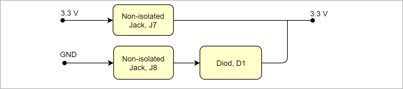 Image Added Image Added
|
|
Power Rails
| Scroll Title |
|---|
| anchor | Table_PWR_PR |
|---|
| title | Module power rails. |
|---|
|
| Scroll Table Layout |
|---|
| orientation | portrait |
|---|
| sortDirection | ASC |
|---|
| repeatTableHeaders | default |
|---|
| style | |
|---|
| widths | |
|---|
| sortByColumn | 1 |
|---|
| sortEnabled | false |
|---|
| cellHighlighting | true |
|---|
|
Power Rail Name | B2B J1 Pins | B2B J2 Pins | B2B J3 Pins | Directions | Note |
|---|
| PL_DCIN | 151, 153, 155, 157, 159 | - | - | Output | - | | DCDCIN | - | 154, 156, 158, 160,
153, 155, 157, 159 | - | Output | - | | LP_DCDC | - | 138, 140, 142, 144 | - | Output | - | | PS_BATT | - | 125 | - | Output | - | | GT_DCDC | - | - | 157, 158, 159, 160 | Output | - | | PLL_3V3 | - | - | 152 | Output | - | | SI_PLL_1V8 | - | - | 151 | Input | - | | PS_1V8 | - | 99 | 147, 148 | Input | - | | PL_1V8 | 91, 121 | - | - | Input | - | | DDR_1V2 | - | 135 | - | Input | - |
|
Board to Board Connectors
| Page properties |
|---|
|
- This section is optional and only for modules.
use "include page" macro and link to the general B2B connector page of the module series, For example: 6 x 6 SoM LSHM B2B Connectors
| Include Page |
|---|
| 6 x 6 SoM LSHM B2B Connectors |
|---|
| 6 x 6 SoM LSHM B2B Connectors |
|---|
|
|
| Include Page |
|---|
| 5.2 x 7.6 UltraSoM+ ST5 and SS5 B2B Connectors |
|---|
| 5.2 x 7.6 UltraSoM+ ST5 and SS5 B2B Connectors |
|---|
|
Technical Specifications
Absolute Maximum Ratings
| Scroll Title |
|---|
| anchor | Table_TS_AMR |
|---|
| title | PS absolute maximum ratings |
|---|
|
| Scroll Table Layout |
|---|
| orientation | portrait |
|---|
| sortDirection | ASC |
|---|
| repeatTableHeaders | default |
|---|
| style | |
|---|
| widths | |
|---|
| sortByColumn | 1 |
|---|
| sortEnabled | false |
|---|
| cellHighlighting | true |
|---|
|
| Symbols | Min | Max | Unit | Note |
|---|
| VIN | -0.3 | 4 | V | VIN is connected directly to module | | Storage Temperatur | -40 | +85 | °C | See DIP Switch, CHS-04TA datasheet |
|
Recommended Operating Conditions
Operating temperature range depends also on customer design and cooling solution. Please contact us for options.
| Scroll Title |
|---|
| anchor | Table_TS_ROC |
|---|
| title | Recommended operating conditions. |
|---|
|
| Scroll Table Layout |
|---|
| orientation | portrait |
|---|
| sortDirection | ASC |
|---|
| repeatTableHeaders | default |
|---|
| style | |
|---|
| widths | |
|---|
| sortByColumn | 1 |
|---|
| sortEnabled | false |
|---|
| cellHighlighting | true |
|---|
|
| Symbols | Min | Max | Unit | Note |
|---|
| VIN | 3,14 | 3.47 | V | Check also TRM of the connected module | | Operating Temperatur | -40 | +85 | °C |
|
|
Physical Dimensions
Module size: 90 mm × 90 mm. Please download the assembly diagram for exact numbers.
Mating height with standard connectors: 3.5 mm.
PCB thickness: 1.6 mm.
| Page properties |
|---|
|
In 'Physical Dimension' section, top and button view of moduloe must be insterted, information regarding physical dimention can be obtained through webpage for product in Shop.Trenz, (Download> Documents> Assembly part)for every SoM. For Example: for Module TE0728, Physical Dimension information can be captured by snipping tools from the link below: https://www.trenz-electronic.de/fileadmin/docs/Trenz_Electronic/Modules_and_Module_Carriers/5.2x7.6/TE0745/REV02/Documents/AD-TE0745-02-30-1I.PDF
|
| Scroll Title |
|---|
| anchor | Figure_TS_PD |
|---|
| title | Physical Dimension |
|---|
|
| Scroll Ignore |
|---|
| draw.io Diagram |
|---|
| border | false |
|---|
| viewerToolbar | true |
|---|
| |
|---|
| fitWindow | false |
|---|
| diagramDisplayName | |
|---|
| lbox | true |
|---|
| revision | 2 |
|---|
| diagramName | TEBT0808_PS_PD |
|---|
| simpleViewer | false |
|---|
| width | |
|---|
| links | auto |
|---|
| tbstyle | hidden |
|---|
| diagramWidth | 641 |
|---|
|
|
| Scroll Only |
|---|
| scroll-pdf | true |
|---|
| scroll-office | true |
|---|
| scroll-chm | true |
|---|
| scroll-docbook | true |
|---|
| scroll-eclipsehelp | true |
|---|
| scroll-epub | true |
|---|
| scroll-html | true |
|---|
| 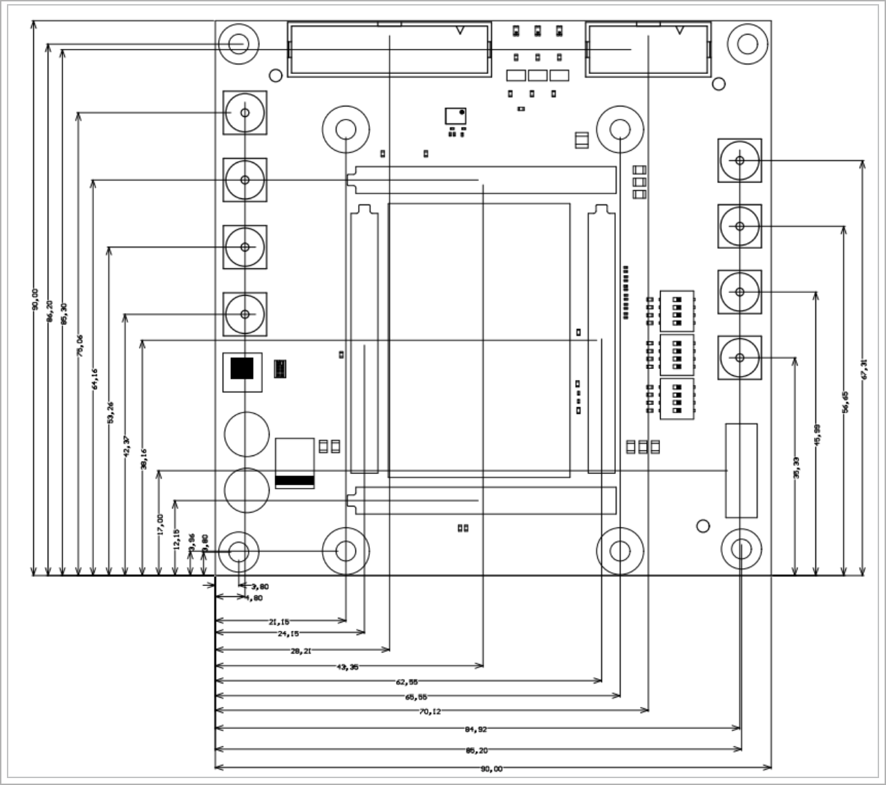 Image Added Image Added
|
|
Currently Offered Variants
| Scroll Title |
|---|
| anchor | Table_VCP_SO |
|---|
| title | Trenz Electronic Shop Overview |
|---|
|
| Scroll Table Layout |
|---|
| orientation | portrait |
|---|
| sortDirection | ASC |
|---|
| repeatTableHeaders | default |
|---|
| style | |
|---|
| widths | |
|---|
| sortByColumn | 1 |
|---|
| sortEnabled | false |
|---|
| cellHighlighting | true |
|---|
|
|
Revision History
Hardware Revision History
| Scroll Title |
|---|
| anchor | Table_RH_HRH |
|---|
| title | Hardware Revision History |
|---|
|
| Scroll Table Layout |
|---|
| orientation | portrait |
|---|
| sortDirection | ASC |
|---|
| repeatTableHeaders | default |
|---|
| style | |
|---|
| widths | |
|---|
| sortByColumn | 1 |
|---|
| sortEnabled | false |
|---|
| cellHighlighting | true |
|---|
|
| Date | Revision | Changes | Documentation Link |
|---|
| 2016-05-30 | 01 | Initial Release | REV01 |
|
Hardware revision number can be found on the PCB board together with the module model number separated by the dash.
| Scroll Title |
|---|
| anchor | Figure_RV_HRN |
|---|
| title | Board hardware revision number. |
|---|
|
| Scroll Ignore |
|---|
| draw.io Diagram |
|---|
| border | false |
|---|
| viewerToolbar | true |
|---|
| |
|---|
| fitWindow | false |
|---|
| diagramDisplayName | |
|---|
| lbox | true |
|---|
| revision | 1 |
|---|
| diagramName | TEBT0808_RV_HRN |
|---|
| simpleViewer | false |
|---|
| width | |
|---|
| links | auto |
|---|
| tbstyle | hidden |
|---|
| diagramWidth | 158 |
|---|
|
|
| Scroll Only |
|---|
| scroll-pdf | true |
|---|
| scroll-office | true |
|---|
| scroll-chm | true |
|---|
| scroll-docbook | true |
|---|
| scroll-eclipsehelp | true |
|---|
| scroll-epub | true |
|---|
| scroll-html | true |
|---|
| 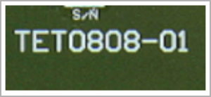 Image Added Image Added
|
|
...
| anchor | Figure_TS_PD |
|---|
| title | Physical Dimension |
|---|
| Scroll Ignore |
|---|
Create DrawIO object here: Attention if you copy from other page, objects are only linked. |
| Scroll Only |
|---|
| scroll-pdf | true |
|---|
| scroll-office | true |
|---|
| scroll-chm | true |
|---|
| scroll-docbook | true |
|---|
| scroll-eclipsehelp | true |
|---|
| scroll-epub | true |
|---|
| scroll-html | true |
|---|
|
image link to the generate DrawIO PNG file of this page. This is a workaround until scroll pdf export bug is fixed |
Currently Offered Variants
...
| anchor | Table_VCP_SO |
|---|
| title | Trenz Electronic Shop Overview |
|---|
...
Revision History
Hardware Revision History
| Scroll Title |
|---|
| anchor | Table_RH_HRH |
|---|
| title | Hardware Revision History |
|---|
|
| Scroll Table Layout |
|---|
|
| orientation | portrait |
|---|
| sortDirection | ASC |
|---|
| repeatTableHeaders | default |
|---|
style | widths | | sortByColumn | 1 |
|---|
| sortEnabled | false |
|---|
| cellHighlighting | true |
|---|
| Date | Revision | Note | PCN |
|---|
- | -
Document Change History
| Page properties |
|---|
|
- Note this list must be only updated, if the document is online on public doc!
- It's semi automatically, so do following
Add new row below first Copy "Page Information Macro(date)" Macro-Preview, Metadata Version number, Author Name and description to the empty row. Important Revision number must be the same as the Wiki document revision number Update Metadata = "Page Information Macro (current-version)" Preview+1 and add Author and change description. --> this point is will be deleted on newer pdf export template - Metadata is only used of compatibility of older exports
|
...
| Scroll Title |
|---|
| anchor | Table_RH_DCH |
|---|
| title | Document change history. |
|---|
|
| Scroll Table Layout |
|---|
| orientation | portrait |
|---|
| sortDirection | ASC |
|---|
| repeatTableHeaders | default |
|---|
| style | |
|---|
| widths | |
|---|
| sortByColumn | 1 |
|---|
| sortEnabled | false |
|---|
| cellHighlighting | true |
|---|
|
| Date | Revision | Contributor | Description |
|---|
| Page info |
|---|
| infoType | Modified date |
|---|
| dateFormat | yyyy-MM-dd |
|---|
| type | Flat |
|---|
|
| | Page info |
|---|
| infoType | Current version |
|---|
| prefix | v. |
|---|
| type | Flat |
|---|
| showVersions | false |
|---|
|
| | Page info |
|---|
| infoType | Modified by |
|---|
| type | Flat |
|---|
| showVersions | false |
|---|
|
change list | | | 2020-05-11 | v.54 | John Hartfiel | add notes to DIP section - Correction on configuration signal section
| | 2020-01-24 | v.49 | Pedram Babakhani | | -- | all | Edit | Page info |
|---|
| infoType | Modified users |
|---|
| type | Flat |
|---|
| showVersions | false |
|---|
|
| |
|
Disclaimer
| Include Page |
|---|
| IN:Legal Notices |
|---|
| IN:Legal Notices |
|---|
|
...